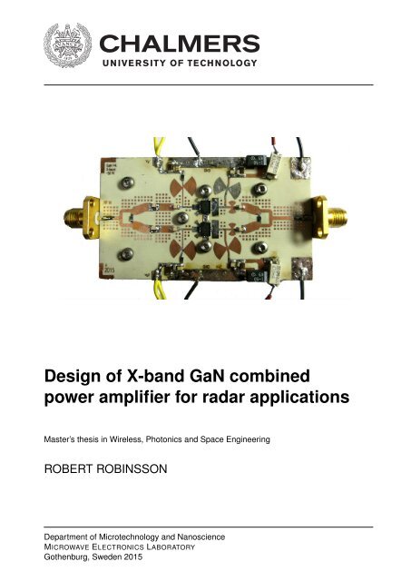
Design of X-band GaN combined power amplifier for radar applications
218368
218368

Create successful ePaper yourself
Turn your PDF publications into a flip-book with our unique Google optimized e-Paper software.
Master’s thesis 2015<strong>Design</strong> <strong>of</strong> X-<strong>band</strong> <strong>GaN</strong> <strong>combined</strong><strong>power</strong> <strong>amplifier</strong> <strong>for</strong> <strong>radar</strong> <strong>applications</strong>ROBERT ROBINSSONDepartment <strong>of</strong> Microtechnology and NanoscienceMicrowave Electronics LaboratoryChalmers University <strong>of</strong> TechnologyGothenburg, Sweden 2015
<strong>Design</strong> <strong>of</strong> X-<strong>band</strong> <strong>GaN</strong> <strong>combined</strong> <strong>power</strong> <strong>amplifier</strong> <strong>for</strong> <strong>radar</strong> <strong>applications</strong>ROBERT ROBINSSON© ROBERT ROBINSSON, 2015.Supervisor: Hannes Illipe, SAAB EDSExaminer: Christian Fager, ChalmersMaster’s Thesis 2015:XXDepartment <strong>of</strong> Microtechnology and NanoscienceMicrowave Electronics LaboratoryChalmers University <strong>of</strong> TechnologySE-412 96 GothenburgTelephone +46 31 772 1000Cover: Fabricated 50 W X-<strong>band</strong> <strong>power</strong> <strong>amplifier</strong> produced during the project.Typeset in L A TEXPrinted by Chalmers ReproserviceGothenburg, Sweden 2015iv
AcknowledgementsI would like to thank my supervisor Hannes Illipe and manager Ingvar Sundvall atthe company SAAB <strong>for</strong> giving me the opportunity to per<strong>for</strong>m this thesis work. Iwould also like to thank the people working at the same department, whom havetaken interest in my work and also been helpful. Finally I would like to thankChristian Fager at Chalmers <strong>for</strong> being my examiner.Robert Robinsson, Gothenburg 2015-06-05vii
Contents1 Introduction 11.1 Purpose . . . . . . . . . . . . . . . . . . . . . . . . . . . . . . . . . . 21.2 Research questions . . . . . . . . . . . . . . . . . . . . . . . . . . . . 21.3 Methods . . . . . . . . . . . . . . . . . . . . . . . . . . . . . . . . . . 21.4 Limitations . . . . . . . . . . . . . . . . . . . . . . . . . . . . . . . . 32 Theory 52.1 Semiconductor devices . . . . . . . . . . . . . . . . . . . . . . . . . . 52.2 <strong>GaN</strong> transistors . . . . . . . . . . . . . . . . . . . . . . . . . . . . . . 52.2.1 HEMT . . . . . . . . . . . . . . . . . . . . . . . . . . . . . . . 62.3 Power <strong>amplifier</strong>s . . . . . . . . . . . . . . . . . . . . . . . . . . . . . . 72.3.1 SSPA and TWTA . . . . . . . . . . . . . . . . . . . . . . . . . 72.3.2 Bias point . . . . . . . . . . . . . . . . . . . . . . . . . . . . . 72.3.3 Stability . . . . . . . . . . . . . . . . . . . . . . . . . . . . . . 82.3.3.1 Stability at non-linear conditions . . . . . . . . . . . 92.3.4 Output <strong>power</strong> . . . . . . . . . . . . . . . . . . . . . . . . . . . 102.3.5 Efficiency . . . . . . . . . . . . . . . . . . . . . . . . . . . . . 102.3.6 Matching network . . . . . . . . . . . . . . . . . . . . . . . . . 102.3.7 Bias network . . . . . . . . . . . . . . . . . . . . . . . . . . . 112.3.8 Substrate . . . . . . . . . . . . . . . . . . . . . . . . . . . . . 112.3.9 Transmission lines . . . . . . . . . . . . . . . . . . . . . . . . 122.3.9.1 Microstrip . . . . . . . . . . . . . . . . . . . . . . . . 122.3.9.2 Stripline . . . . . . . . . . . . . . . . . . . . . . . . . 122.3.9.3 Coplanar waveguide . . . . . . . . . . . . . . . . . . 122.3.10 Lumped components . . . . . . . . . . . . . . . . . . . . . . . 132.3.10.1 Capacitors . . . . . . . . . . . . . . . . . . . . . . . 132.3.10.2 Inductors . . . . . . . . . . . . . . . . . . . . . . . . 142.3.10.3 Resistors . . . . . . . . . . . . . . . . . . . . . . . . 142.3.11 RF drive signal . . . . . . . . . . . . . . . . . . . . . . . . . . 142.3.12 Device failure . . . . . . . . . . . . . . . . . . . . . . . . . . . 142.4 Combining network . . . . . . . . . . . . . . . . . . . . . . . . . . . . 152.4.1 Wilkinson divider . . . . . . . . . . . . . . . . . . . . . . . . . 152.4.2 90 ◦ hybrid . . . . . . . . . . . . . . . . . . . . . . . . . . . . . 162.4.3 180 ◦ hybrid . . . . . . . . . . . . . . . . . . . . . . . . . . . . 172.4.4 Bus bar combiner . . . . . . . . . . . . . . . . . . . . . . . . . 172.4.5 Parallel matching network . . . . . . . . . . . . . . . . . . . . 17ix
Contents2.4.6 Distributed <strong>amplifier</strong> . . . . . . . . . . . . . . . . . . . . . . . 172.5 Simulation and models . . . . . . . . . . . . . . . . . . . . . . . . . . 183 Methods 213.1 Per<strong>for</strong>mance requirements . . . . . . . . . . . . . . . . . . . . . . . . 213.2 Analysis <strong>of</strong> reference <strong>amplifier</strong> . . . . . . . . . . . . . . . . . . . . . . 213.3 <strong>Design</strong> <strong>of</strong> prototype . . . . . . . . . . . . . . . . . . . . . . . . . . . . 233.3.1 Substrate material . . . . . . . . . . . . . . . . . . . . . . . . 233.3.2 DC characteristics and bias point . . . . . . . . . . . . . . . . 233.3.3 Stability . . . . . . . . . . . . . . . . . . . . . . . . . . . . . . 243.3.4 Source and load reflection coefficient . . . . . . . . . . . . . . 243.3.5 Matching network . . . . . . . . . . . . . . . . . . . . . . . . . 263.3.6 Bias network . . . . . . . . . . . . . . . . . . . . . . . . . . . 263.3.7 Combining network . . . . . . . . . . . . . . . . . . . . . . . . 273.3.8 Coupling capacitors . . . . . . . . . . . . . . . . . . . . . . . . 283.3.9 Transistor footprint . . . . . . . . . . . . . . . . . . . . . . . . 283.3.10 Electromagnetic simulation . . . . . . . . . . . . . . . . . . . 283.3.11 Test boards . . . . . . . . . . . . . . . . . . . . . . . . . . . . 293.3.12 Stability with applied input <strong>power</strong> . . . . . . . . . . . . . . . 323.3.13 Final optimization and adjustments . . . . . . . . . . . . . . . 323.4 Fabrication <strong>of</strong> prototype . . . . . . . . . . . . . . . . . . . . . . . . . 393.4.1 Printed circuit board . . . . . . . . . . . . . . . . . . . . . . . 393.4.2 Connectors . . . . . . . . . . . . . . . . . . . . . . . . . . . . 403.4.3 Soldering and assembly . . . . . . . . . . . . . . . . . . . . . . 403.4.4 Mounting fixture . . . . . . . . . . . . . . . . . . . . . . . . . 413.4.5 Verification and troubleshooting . . . . . . . . . . . . . . . . . 413.4.6 Tuning and setup . . . . . . . . . . . . . . . . . . . . . . . . . 423.5 Measurements on prototype . . . . . . . . . . . . . . . . . . . . . . . 423.5.1 S-parameter measurements . . . . . . . . . . . . . . . . . . . . 443.5.2 Power measurements . . . . . . . . . . . . . . . . . . . . . . . 453.5.3 Error sources . . . . . . . . . . . . . . . . . . . . . . . . . . . 464 Results 474.1 S-parameters . . . . . . . . . . . . . . . . . . . . . . . . . . . . . . . 474.2 Output <strong>power</strong> . . . . . . . . . . . . . . . . . . . . . . . . . . . . . . . 474.3 Device temperature . . . . . . . . . . . . . . . . . . . . . . . . . . . . 475 Discussion 536 Conclusion 55A Measurement equipmentIx
1IntroductionThe need <strong>for</strong> more efficient electronic circuitry is always evolving [1]. Electronicsystems typically consists <strong>of</strong> several blocks per<strong>for</strong>ming different tasks. Some blocksconsume more <strong>power</strong> than others. The efficiency <strong>of</strong> the entire circuit can be increasedif the <strong>power</strong> consumption <strong>of</strong> these circuit elements can be decreased.Microwave circuits are used to generate and amplify RF <strong>power</strong> <strong>for</strong> use in a wirelesssystem, i.e. a communication or <strong>radar</strong> system. A majority <strong>of</strong> the energy will typicallybe used by the <strong>power</strong> <strong>amplifier</strong> in these systems. It is thus very important to keepthe efficiency <strong>of</strong> the <strong>power</strong> <strong>amplifier</strong> high to lower the <strong>power</strong> consumption <strong>of</strong> theentire system [2]. The wasted energy will otherwise turn into heat that will have tobe conducted away from the circuit using cooling solutions.A typical <strong>radar</strong> system operates with high output <strong>power</strong> in order to increase therange and detection probability <strong>of</strong> targets [3]. Semiconductor based <strong>amplifier</strong>s havein the past not been used to achieve very high <strong>power</strong> levels at high frequency.Vacuum electron devices have instead been used to make <strong>amplifier</strong>s that can operateat high <strong>power</strong> levels [4]. One such device is the travelling wave tube (TWT), a bigand bulky device that require high voltage to run. They also have a lot <strong>of</strong> mechanicalparts in them that could fail.Semiconductor devices on the other hand can be small in size and reliable. Researchand development in the field <strong>of</strong> semiconductor devices have enabled fabrication <strong>of</strong>transistors that could compete with some <strong>of</strong> the vacuum devices in terms <strong>of</strong> output<strong>power</strong>. These breakthroughs in semiconductor research have enabled fabrication <strong>of</strong>gallium nitride (<strong>GaN</strong>) based transistors that can be operated at higher <strong>power</strong> levels[5].Gallium nitride transistors can operate at high <strong>power</strong> levels due to their high <strong>power</strong>density and at high frequency due to the high electron mobility transistor (HEMT)transistor architecture [4]. The development <strong>of</strong> <strong>GaN</strong> HEMTs have been rapid andthe output <strong>power</strong> level <strong>of</strong> a device can be high even at microwave frequencies. This iswhy <strong>GaN</strong> devices can outper<strong>for</strong>m other popular semiconductor materials as galliumarsenide (GaAs) and silicon (Si) in terms <strong>of</strong> <strong>power</strong> and efficiency [6].The <strong>power</strong> level can further be increased by combining multiple transistors in parallel.This requires combining networks to be used that can feed all transistors withthe input signal and then sum the signal at the output. GaAs transistors have beenused during a longer period, but it is becoming difficult to achieve high <strong>power</strong> levelswith this technique. Multiple transistors have to be <strong>combined</strong> at once, but losses inthe combining network itself will also be higher when the number <strong>of</strong> devices grow.There is no advantage in combining too many transistors due to this effect, sincemore and more <strong>power</strong> will be lost [6]. The combining network must there<strong>for</strong>e be1
1. Introductionoptimized to have as small loss as possible to ensure maximum output <strong>power</strong>.The transistor must also be matched with using a matching network and suppliedwith <strong>power</strong> through a bias network. These three circuit elements together with thetransistor itself will <strong>for</strong>m the major parts <strong>of</strong> the <strong>combined</strong> microwave <strong>amplifier</strong>.There are pre-matched 50 Ω <strong>GaN</strong> <strong>amplifier</strong>s blocks available on the market <strong>for</strong> useas <strong>power</strong> <strong>amplifier</strong>s, but their cost is rather high. A more cost effective solutioncould be to use ordinary unmatched <strong>GaN</strong> transistors along with a custom combining,matching and bias network designed <strong>for</strong> them. Output <strong>power</strong> and efficiencyare the most important per<strong>for</strong>mance figures if considering requirements <strong>for</strong> <strong>radar</strong><strong>applications</strong>.1.1 PurposeThe purpose <strong>of</strong> the project is to investigate if unmatched <strong>GaN</strong> transistors can beused to fabricate an X-<strong>band</strong> <strong>power</strong> <strong>amplifier</strong> with output <strong>power</strong> up to 50 W. The finalprototype will be characterized by measurements to see how well it could per<strong>for</strong>m.1.2 Research questionsA number <strong>of</strong> questions have been looked into to reach the goal and fulfil the purpose<strong>of</strong> the project:• What type <strong>of</strong> combining network should be used to combine multiple transistorsin parallel?• How can losses in the combining network be minimized?• What type <strong>of</strong> matching network should be used?• How should the transistor be biased?• How should the bias network be designed?• What will happen during failure <strong>of</strong> one or more transistor?• On what substrate material should the circuit be built on?• How should oscillations be prevented?• How small in size can the circuit be?1.3 MethodsA literature review <strong>of</strong> the subject was first per<strong>for</strong>med to gain knowledge on how todesign the <strong>amplifier</strong> and its combining networks. Books and research papers havemainly been used to gather in<strong>for</strong>mation about the topic. The in<strong>for</strong>mation obtainedduring this study have been used to decide how the following design project shouldevolve.The next step in the project was to per<strong>for</strong>m simulations using a computer baseddesign tool called Microwave Office, a program especially suited <strong>for</strong> microwave designwork. A non-linear model <strong>of</strong> the transistor have been available <strong>for</strong> use with thesimulation s<strong>of</strong>tware. Different variants <strong>of</strong> combining networks have been evaluatedin order to find a suitable design <strong>for</strong> combination <strong>of</strong> multiple transistors. Individual2
1. Introductioncomponents <strong>of</strong> the <strong>amplifier</strong> have been simulated as independent modular blocks toa large extent to make the design process less complex. Circuit blocks have thenbeen fitted together to <strong>for</strong>m a complete <strong>power</strong> <strong>amplifier</strong>.A 50 W X-<strong>band</strong> <strong>power</strong> <strong>amplifier</strong> was then constructed using the unmatched transistor.Each transistor is capable <strong>of</strong> delivering 25 W. The prototype is there<strong>for</strong>e usingtwo transistors connected in parallel, since usage <strong>of</strong> more transistors would make theproject too complex <strong>for</strong> practical construction. The prototype has been manufacturedas a surface mount board with lumped components and distributed elementson a printed copper circuit board. Measurements on the prototype were per<strong>for</strong>medto investigate how well the per<strong>for</strong>mance compared with that <strong>of</strong> the simulated circuit.The findings <strong>of</strong> the project have been documented in this report during the entirelength <strong>of</strong> the project to capture the entire process as complete as possible.1.4 LimitationsThe main tool used <strong>for</strong> the circuit design have been Microwave Office and the suppliedtransistor model <strong>for</strong> it. The project has been limited by the capabilities <strong>of</strong> thes<strong>of</strong>tware and the model as they are based on assumptions that approximate the realworld behaviour <strong>of</strong> the device.The project has also been limited by the fabrication techniques available <strong>for</strong> prototyping.Commercial processes can <strong>of</strong>fer higher quality boards, but the fabricationtime needed would have delayed the project. Multiple test boards have been possibleto fabricate during the project because <strong>of</strong> the short manufacturing time.3
1. Introduction4
2TheoryThis chapter will discuss the theory behind the design and construction process <strong>of</strong>the project. The reader <strong>of</strong> this section is assumed to have some knowledge regardingbasic microwave engineering to be able to follow the concepts presented.2.1 Semiconductor devicesSemiconductor devices are today very popular <strong>for</strong> use in electronic devices <strong>of</strong> all categories.Transistors and diodes are the most common semiconductor based electricalcomponents. They are widely used in digital electronics, but also very frequentlyused in analog circuits [7]. Microwave circuits require special transistors to be usedthat can operate at high frequency with reasonable per<strong>for</strong>mance.The transistor is a non-linear three terminal device, i.e. Ohm’s law can not beused to analyze the electrical properties <strong>of</strong> the device. There exists two main types<strong>of</strong> transistors, the bipolar junction transistor (BJT) and the field effect transistor(FET) [7]. The BJT has a collector, base and emitter terminal. The collectorcurrent is controlled by an input current at the base. The FET has a drain, gateand source terminal, but the drain current is instead controlled by a voltage appliedto the gate.The BJT and FET devices can both be found in modern circuits. They are differentand there are uses <strong>for</strong> both <strong>of</strong> them depending on the application. Modernsemiconductor materials like <strong>GaN</strong> are used to create FET devices, with no bipolarequivalent.The FET family <strong>of</strong> devices is itself divided into different categories. The high electronmobility transistor (HEMT) is the semiconductor architecture used when fabricating<strong>GaN</strong> transistors [4].The most common use <strong>for</strong> transistors in analog microwave circuits is as an <strong>amplifier</strong>.The transistor is typically used as a variable resistor when it is used in analogcircuitry [4]. An applied input signal on the gate will control the amount <strong>of</strong> currentflowing through the transistor. A signal with a small amplitude applied to the gatecan in this way generate a larger amplitude output signal at the drain side <strong>of</strong> thetransistor [8]. This is the basic principle when using transistors to amplify signals.2.2 <strong>GaN</strong> transistorsGallium nitride (<strong>GaN</strong>) transistors are becoming more and more used in microwave<strong>applications</strong> because <strong>of</strong> their high per<strong>for</strong>mance figures compared to other semicon-5
2. TheoryFigure 2.1: Basic layer structure <strong>of</strong> a <strong>GaN</strong> HEMT.ductor materials used earlier [4]. Research about the semiconductor material acceleratedduring the 1990’s along with development <strong>of</strong> new methods to grow thematerial on other substrates [5]. GaAs transistors have been and are still very popular<strong>for</strong> use in microwave circuits, but <strong>GaN</strong> transistors will and have replaced theGaAs transistor in many circuits.The <strong>GaN</strong> technology is still relatively young and development <strong>of</strong> device fabricationmethods are still moving ahead. A new technology is <strong>of</strong>ten expensive to implementin the beginning, but the per<strong>for</strong>mance increase can make it worth in long term.Reliability is always a concern when selecting devices <strong>for</strong> use in a circuit. <strong>GaN</strong>devices have still not been tested in the field <strong>for</strong> long time periods [9]. This factmay exclude <strong>GaN</strong> transistors to be used within some application areas.<strong>GaN</strong> is a semiconductor material with very high <strong>power</strong> density, hence it can be usedto produce transistors with high output <strong>power</strong>. The material can also withstandhigh electric fields be<strong>for</strong>e breaking down [5]. The efficiency can be very high sincethe resistance during the on state is low. The drain-source voltage can be high sincethe device can tolerate high electric fields. The drain current can thus be loweredand losses can be decreased since they are heavily dependent on the current. Theparasitic capacitance at the input and output is low, making matching the deviceto another impedance more easy [5].2.2.1 HEMTThe high-electron-mobility transistor or HEMT is the type <strong>of</strong> transistor manufacturedbased on <strong>GaN</strong>. The <strong>GaN</strong> HEMT device is a hetrostructure <strong>of</strong> two semiconductors,<strong>GaN</strong> and Al<strong>GaN</strong>, see figure 2.1. A two dimensional electron gas is <strong>for</strong>med inthe intrinsic region between the two sandwiched semiconductors. The electrons aretrapped in this region and they can only move freely in this plane while the transistorsis active [4]. The active channel where the electrons are moving is undopedor intrinsic. This enables the electrons to move fast through the transistor sinceno collisions involving dopants occur. This will also make the channel resistancevery low during the active state. Less <strong>power</strong> will there<strong>for</strong>e be dissipated over thetransistor [4]. This <strong>power</strong> could instead be delivered to the load.6
2. Theory<strong>GaN</strong> devices are today typically grown on either silicon carbide (SiC) or silicon(Si) substrates. <strong>GaN</strong> grown on SiC is superior when considering parameters such asthermal and <strong>power</strong> per<strong>for</strong>mance. SiC have a very high thermal conductivity and canact as a heat sink to conduct heat away from the active channel <strong>of</strong> the transistor.<strong>GaN</strong> on Si on the other hand is a cost effective solution since the fabrication processis well developed and Si wafers can be bought <strong>for</strong> a low price [5].2.3 Power <strong>amplifier</strong>sPower <strong>amplifier</strong>s are used to amplify an input signal and output a signal with higher<strong>power</strong>. The gain <strong>of</strong> the device is not always very high, but the <strong>amplifier</strong> must be ableto source enough <strong>of</strong> <strong>power</strong> to the load without going into saturation. A microwave<strong>amplifier</strong> design have to be executed with special care to the effects occurring atthe higher frequency. The design must take reflections into consideration when thewavelength <strong>of</strong> the signal approaches the circuit size [10].Power <strong>amplifier</strong>s have to be able to output a high output <strong>power</strong>, while still maintaininghigh efficiency. Special design considerations have to be introduced, notused when designing a more general <strong>amplifier</strong>. These should help maximize theoutput <strong>power</strong> and efficiency <strong>of</strong> the <strong>amplifier</strong>. These methods mostly concern theconfiguration <strong>of</strong> the components used on the drain side <strong>of</strong> the transistor [10].2.3.1 SSPA and TWTASemiconductor devices are not the only device historically used to construct <strong>power</strong><strong>amplifier</strong>s <strong>for</strong> microwave <strong>applications</strong>. The travelling wave tube <strong>amplifier</strong> (TWTA)can output a high <strong>power</strong> at very high frequencies. The solid state <strong>power</strong> <strong>amplifier</strong>(SSPA) have historically only been used at relatively low frequencies and low <strong>power</strong>levels [11]. The <strong>GaN</strong> technology have during recent years made the SSPA technologymore interesting and the competition between the SSPA and TWTA have becomemore equal.Replacing vacuum tubes with solid state devices have been a goal <strong>for</strong> many researchesand circuit designers. The main disadvantage using the TWTA is its reliability.Mechanical parts inside the TWTA are sensitive and prone to failure. The tubeitself will wear out after a certain time and a replacement must be installed [11]. Ahigh voltage <strong>power</strong> supply must be used to operate the TWTA. This is both unsafeand the complexity <strong>of</strong> the <strong>power</strong> supply can be high.Solid state devices have proven more and more useful in <strong>applications</strong> that be<strong>for</strong>e onlyrelied on vacuum tubes. SSPA can be made smaller to shrink the entire size <strong>of</strong> thedevice using it. This is important in modern wireless <strong>applications</strong> where the <strong>power</strong><strong>amplifier</strong> <strong>of</strong>ten is mounted in an antenna array. Overall efficiency can also increaseto eliminate heat problems when mounting the circuitry in a dense environment.2.3.2 Bias pointA DC voltage is applied to the gate and source <strong>of</strong> the transistor to set the bias point<strong>of</strong> the device. The bias voltage will enable the transistor to operate with a small7
2. TheoryRF input signal. The RF signal would otherwise not be able to set the transistor tooperate in the active region, this would result in a very distorted signal or in worstcase no output signal at all. The DC operating point is a very important parameterthat will determine the RF per<strong>for</strong>mance <strong>of</strong> the <strong>amplifier</strong> to a large extent [2].Table 2.1: Summary <strong>of</strong> <strong>amplifier</strong> classes.ClassAABBCConduction angle360 ◦180 ◦ -360 ◦180 ◦< 180 ◦The chosen bias point can be adjusted to change the per<strong>for</strong>mance <strong>of</strong> the <strong>amplifier</strong>drastically. Different classes have been used to name these operating modes. Theclass is determined by how long during a full cycle the transistor will conduct whenan RF signal is applied at the input. Table 2.1 shows a summary <strong>of</strong> some <strong>amplifier</strong>classes. There are other classes, but they are switched <strong>amplifier</strong>s [12].The bias point and class will determine how efficient the <strong>amplifier</strong> can be. A class Atype <strong>of</strong> <strong>amplifier</strong> will be most inefficient, while a class C <strong>amplifier</strong> will be the mostefficient. Distortion will be the disadvantage when increasing the efficiency by thismethod.2.3.3 StabilityThe <strong>amplifier</strong> will oscillate if it is unstable. This could cause the device to selfdestruct or damage surrounding components [10]. Stability <strong>of</strong> the transistor is dependenton the amount <strong>of</strong> <strong>power</strong> reflected back from the active device. The transistoris unstable if more <strong>power</strong> is reflected back than is fed towards the transistor. Thiscan happen if the impedance on the input or output port have a negative real part.This would result in reflection coefficients |Γ in | > 1 or |Γ out | > 1 [2]. This is thegeneral condition <strong>for</strong> instability.Stability is classified into two categories, unconditionally stable and conditionallystable devices.An unconditionally stable transistor will be stable independently <strong>of</strong> what terminationsare applied to the input or output ports. A conditionally stable transistor isonly stable <strong>for</strong> a limited range <strong>of</strong> terminations.A few tools and methods are available to analyze the stability <strong>of</strong> a circuit. The mostcommon are based on calculations using scattering parameters <strong>of</strong> the transistor.Rollet’s condition is one <strong>of</strong> these, defined asK = 1 − |S 11| 2 + |S 22 | 2 + |∆| 22|S 12 S 21 |> 1where ∆ is|∆| = |S 11 S 22 − S 12 S 21 | < 1These two conditions indicate if the transistor is stable or unstable [2].8
2. TheoryAnother stability condition involves just a single parameter [13]. It is defined asµ =1 − |S 11 | 2|S 22 − ∆S 11 ∗ | + |S 12 S 21 | > 1There are several methods <strong>of</strong> making an unstable transistor stable [14]. A feedbacknetwork can be constructed to make the transistor stable. A resistor can also beplaced at the gate or drain either in series or parallel. This will load the transistorand make the <strong>amplifier</strong> stable. It is a bad idea to place a resistor on the drainside when developing a <strong>power</strong> <strong>amplifier</strong> since it would dissipate much <strong>of</strong> the output<strong>power</strong>.2.3.3.1 Stability at non-linear conditionsIt is not enough to just examine the stability <strong>of</strong> the circuit when no input signal isapplied. The circuit could be stable when per<strong>for</strong>ming an analysis based on smallsignals-parameters, but become unstable when driven with a large input signal [15].The input signal will change the characteristics <strong>of</strong> the non-linear device. A harmonicbalance simulation is <strong>of</strong>ten per<strong>for</strong>med to investigate the per<strong>for</strong>mance <strong>of</strong> a non-linearcircuit, but this method can only be used to find oscillations harmonically relatedto the input signal [15].A method to find such an unwanted oscillation must be utilized to examine if thecircuit will be stable with different levels <strong>of</strong> input <strong>power</strong> applied. A method calledthe auxiliary generator technique is one way to per<strong>for</strong>m such a simulation [15]. Thismethod is based on a local stability analysis <strong>of</strong> a circuit, where nodes in the circuitare examined to check <strong>for</strong> unwanted oscillations. This technique is convenient touse on circuits as <strong>power</strong> <strong>amplifier</strong>s, since they <strong>of</strong>ten are driven hard into non-linearoperation.The auxiliary generator method is simple to implement using standard tools inMicrowave Office. A sinusoidal voltage source is connected to a node in the circuitto be examined. The voltage amplitude and phase <strong>of</strong> the signal source is set tobe constant, while the frequency f ag can be swept. The current is measured with acurrent probe at the same point. The admittance at the test point can be calculatedsimply asY test point = I test pointV test pointThe value <strong>of</strong> the admittance can be used to find a point where it approaches zero.This happens if the current flowing through the test probe approaches zero. Thecondition to look <strong>for</strong> isY test point = I test pointV test point= 0 + j0Potential unstable frequencies can be found by per<strong>for</strong>ming a sweep <strong>of</strong> the generatorfrequency f ag while looking <strong>for</strong> the above condition to become true.9
2. Theory2.3.4 Output <strong>power</strong>Output <strong>power</strong> can be maximized by following a few principles when designing the<strong>amplifier</strong> circuit. These methods will define how the matching networks later have tobe designed. The input <strong>of</strong> the transistor should be terminated to allow <strong>for</strong> maximumgain [14]. This will occur whenΓ in = Γ ∗ SThe output could also be terminated in the same way, according toΓ out = Γ ∗ Lif the <strong>amplifier</strong> was to be designed <strong>for</strong> the maximum amount <strong>of</strong> gain.A <strong>power</strong> <strong>amplifier</strong> should not have maximum gain as the main requirement, butoutput <strong>power</strong> should instead be the main concern. The input could be designedfollowing the method above, but the output termination should be constructed in adifferent way. Maximum output <strong>power</strong> will be reached when the voltage and currentswing at the output <strong>of</strong> the transistor is maximized. The output <strong>of</strong> the transistorneeds to see a specific load impedance in order <strong>for</strong> this to occur. This type <strong>of</strong> load isreferred to as a Cripps load. A Cripps load will place the load line <strong>of</strong> the transistorin a way that maximizes the output <strong>power</strong> [12].This method will ideally produce an <strong>amplifier</strong> that can deliver the maximum amount<strong>of</strong> <strong>power</strong> to the load. Losses are not taken into account, but they will also affect the<strong>power</strong> per<strong>for</strong>mance.2.3.5 EfficiencyThe efficiency <strong>of</strong> the <strong>amplifier</strong> is a measure <strong>of</strong> how much <strong>of</strong> the input RF <strong>power</strong>and DC supply <strong>power</strong> that is converted into usable RF output <strong>power</strong> [12]. Lesswasted <strong>power</strong> in the device will make it more efficient. The efficiency is determinedby measuring both the consumed DC <strong>power</strong> and the RF output <strong>power</strong>. The drainefficiency η is defined asη = P RFP DCAnother popular measure takes the added input RF <strong>power</strong> into consideration. It isreferred to as the <strong>power</strong> added efficiency (PAE), given by2.3.6 Matching networkP AE = P RF,out − P RF,inP DCMatching networks are needed at the input and output <strong>of</strong> the transistor to trans<strong>for</strong>mthe impedance <strong>of</strong> the source and load to the impedance required on the input andoutput <strong>of</strong> the transistor. This is per<strong>for</strong>med in order to eliminate or at least minimizethe reflections present otherwise [6].The matching network can be realized in many different ways. Lumped componentssuch as capacitors and inductors can be used <strong>for</strong> lossless matching networks in the10
2. Theoryideal case. Resistors can be used in some cases, but they will introduce lossesin the matching network. Distributed components are the alternative to lumpedcomponents. Lumped components are more complex to use at higher frequenciessince parasitic effects become a problem [2]. Distributed elements on the other handbecome very large in size if the frequency is low. The right strategy have to be useddepending on the operation frequency <strong>of</strong> the circuit.The <strong>band</strong>width over which the matching network can operate properly should be aswide as possible. This can be hard to realize in reality. Wide <strong>band</strong>width matchingnetworks will typically increase in size, a compromise must there<strong>for</strong>e be made [6].2.3.7 Bias networkThe bias network should supply the DC <strong>power</strong> needed to run the transistor. Thebias network should also isolate the DC <strong>power</strong> supply from RF energy [2]. The biassupply must remain stable even if the current drawn by the <strong>amplifier</strong> can vary. Thisis especially important at the gate, where the bias point could be altered otherwise.The bias network will if constructed correctly stabilize the the <strong>amplifier</strong>. Relativelylong wires are <strong>of</strong>ten used to connect the circuit to the <strong>power</strong> supply. These wiresare inductive and could potentially <strong>for</strong>m a LC-tank together with the capacitorsin the <strong>power</strong> supply. The LC-tank could introduce oscillations at its resonancefrequency [8]. A battery <strong>of</strong> capacitors could be placed near the DC fed point <strong>of</strong> thebias network to counter act this process. Different values <strong>of</strong> capacitors are used toensure capacitive properties over a wide <strong>band</strong>width.The bias network should supply the transistor with current even when the <strong>power</strong>supply can not keep up. The peak current is taken from the capacitors and the<strong>power</strong> supply will deliver the average current drawn [6].Large currents will sometimes be sourced from the drain supply. The microstriptrace must be able to handle this current passing through the network withoutheating up to much. The microstrip trace could otherwise be destroyed by excessivetemperatures.Some active circuitry could also be added to protect the transistor from being destroyedbeyond recovery. This protection function should limit the current drawnby both the gate and drain within safe operating limits.2.3.8 SubstrateThe surface mount <strong>amplifier</strong> circuit is built on a circuit board. The circuit boardis made using a dielectric substrate material covered with a thin layer <strong>of</strong> metal onthe top and bottom. The backside metal layer is usually left untouched to <strong>for</strong>m aground plane <strong>for</strong> the circuit. The top metal layer is etched according to the designlayout. Surface mount components and other packages could then be soldered tothe top <strong>of</strong> the board [16].The substrate can be made using different dielectric materials. The substrate materialmust be selected according to the application considered. The top metal layer ismade <strong>of</strong> copper, sometimes with a thin layer <strong>of</strong> some other metal to protect it. Thethickness <strong>of</strong> the substrate and metal layer can also be chosen by the designer. The11
2. TheoryFigure 2.2: Three common types <strong>of</strong> transmission lines, microstrip, stripline andcoplanar waveguide.size <strong>of</strong> the circuit and the losses will be affected by the type <strong>of</strong> substrate materialchosen [2].2.3.9 Transmission linesTransmission lines must be used to guide the electromagnetic energy to a desiredlocation on the circuit board. Different alternatives exists, but three major ones arecommon <strong>for</strong> printed circuit board construction. These are illustrated in figure 2.2.Losses will always be present in a non ideal transmission line, independent on howgood the design is. Losses can be controlled and reduced by careful selection <strong>of</strong> thephysical structure <strong>of</strong> the transmission line as well as what materials that are usedto fabricate it. Losses occur because <strong>of</strong> different reasons [6]. Losses can be presentin the dielectric material or in the metal layer. Radiation losses can also occur, butthey depend a lot on the layout used. Antennas could <strong>for</strong> example be manufacturedas transmission lines on a circuit board. These should have very high radiationlosses.2.3.9.1 MicrostripThe microstrip line is placed on a substrate <strong>of</strong> dielectric material with a groundplane on the bottom. The characteristic impedance <strong>of</strong> the line is determined by thewidth <strong>of</strong> the line. The thickness <strong>of</strong> the metal layer and the substrate will also befactors affecting the electrical per<strong>for</strong>mance <strong>of</strong> the microstrip line [2].2.3.9.2 StriplineA stripline transmission line is similar in structure to a microstrip, but a substrateand ground layer is also place on top <strong>of</strong> the center conductor to fully confine thefield between two layers <strong>of</strong> dielectric materials and ground planes.2.3.9.3 Coplanar waveguideThe coplanar waveguide transmission line is similar to the microstrip structure, buta top ground plane have been added in the same plane as the top conductor. Thetop ground plane is placed close to the top transmission line with some spacing toconfine the fields as much as possible.12
2. Theory(a) Resistor(b) Capacitor(c) InductorFigure 2.3: Basic equivalent circuits <strong>of</strong> a resistor, capacitor and inductor.2.3.10 Lumped componentsPassive components such as resistors, capacitors and inductors have to be used wheredistributed elements can not be implemented. These components should in theorybe ideal, but they are in practice more complex. Parasitic circuit elements will bepresent in all physical components. The equivalent circuit <strong>of</strong> a typical non-idealcomponent will contain other parasitic components [8]. Basic equivalent circuitsrepresenting these parasitics are shown in figure 2.3.These parasitic effects can cause problems since self oscillations may occur at aspecific frequency. It is there<strong>for</strong>e important to take the parasitic effects into considerationwhen designing circuits. The passive will not oscillate by itself, but improperdesign <strong>of</strong> the circuit can excite the component and cause an unwanted oscillation tostart [6].Most lumped components are available as surface mounted chips to be soldereddirectly to the circuit board. The size may differ depending on the componentvalue, but standard sizes are available.The size <strong>of</strong> the lumped component should be small compared to the wavelength <strong>of</strong> thesignal applied to it. The component must otherwise be considered as a distributedelement [6].2.3.10.1 CapacitorsCapacitors are important components in a microwave circuit. They can be used todecouple and smooth out DC voltages. They can also be used to block DC andcouple the RF signal between sections <strong>of</strong> a circuit [6].Capacitors have a serial and a parallel resonance frequency. The capacitor willhave no reactive part at the series resonance frequency, hence it will have its lowestimpedance at this frequency [17]. The insertion loss <strong>of</strong> the capacitor will thus beat its lowest. This is useful when capacitors are are placed in series with an RFtransmission line, i.e. as a coupling capacitor to couple <strong>power</strong> from one part <strong>of</strong> thecircuit to another.13
2. Theory2.3.10.2 InductorsInductors can be used to block RF signals and conduct DC signals, they can alsobe used <strong>for</strong> matching. It is difficult to utilized surface mount inductors operatingat high frequency, due to the large stray capacitance [17]. This capacitance willcause the inductor to have a self-resonant frequency. The inductor will be seen asa capacitor and not work as expected above this frequency. It is not practical touse inductors when designing circuits <strong>for</strong> high frequency operation because <strong>of</strong> thisproperty [17].2.3.10.3 ResistorsResistors have a wide variety <strong>of</strong> uses in microwave circuits. They can by introducingloss dissipate unwanted <strong>power</strong> in circuits or used to stabilize an unstable circuit[6]. Resistors are in practice always associated with some stray capacitance andinductance. This may cause the resistor to act very differently at higher frequencies[17].2.3.11 RF drive signalThe input drive signal will supply the <strong>amplifier</strong> with input <strong>power</strong>. The <strong>power</strong> level<strong>of</strong> the input signal must be sufficiently large since the <strong>power</strong> gain <strong>of</strong> a typical <strong>power</strong><strong>amplifier</strong> can be relatively low.The input signal can be a continuous wave (CW) or a pulsed type <strong>of</strong> signal. Apulsed input signal will be switched on <strong>for</strong> a limited time during a period, called theduty cycle. The duty cycle is <strong>of</strong>ten expressed in terms <strong>of</strong> percent.A pulsed input signal will lower the overall average <strong>power</strong> dissipated in the <strong>amplifier</strong>.This will lower the thermal stress on the <strong>amplifier</strong> compared to when feeding the<strong>amplifier</strong> with a CW input signal [6].The bias supply <strong>for</strong> the <strong>amplifier</strong> can also be switched on and <strong>of</strong>f together with theinput RF <strong>power</strong>. The bias supply must be turned on slightly be<strong>for</strong>e the input signalis applied, since the bias network must have some time to charge up. The overallefficiency <strong>of</strong> the <strong>amplifier</strong> will be improved when switching the bias supply, since no<strong>power</strong> is dissipated when the input RF signal is turned <strong>of</strong>f.A <strong>power</strong> <strong>amplifier</strong> <strong>for</strong> use in a <strong>radar</strong> system is <strong>of</strong>ten operated with a pulsed inputsignal [6].2.3.12 Device failureCatastrophic failure <strong>of</strong> a transistor used in a <strong>power</strong> <strong>combined</strong> <strong>amplifier</strong> will degradethe per<strong>for</strong>mance in some way, but the <strong>amplifier</strong> could in theory continue to operateat some level. The faulty transistor will change its electrical properties and be seenas a short circuit or in most cases an open circuit. This will change the impedanceseen by external networks connected to the transistor [6]. This may cause severe<strong>power</strong> reflection to occur that may destroy external components along the way. Thecircuit must there<strong>for</strong>e be constructed with robust components that can handle theextra stress applied in such a case.14
2. TheoryPort 1√2Z0 λ/4√2Z0 λ/42Z 0Port 2Port 3Figure 2.4: Circuit topology <strong>of</strong> a two-way Wilkinson <strong>power</strong> divider.The <strong>amplifier</strong> developed in this work will not be designed to withstand a failure.This is not needed in all cases, since the entire <strong>amplifier</strong> could be replaced insteadif a failure was to occur.2.4 Combining networkA combining network should enable N number <strong>of</strong> transistors to be connected to asingle source and load. This passive device will split or combine the <strong>power</strong> <strong>of</strong> asingle device and distribute it to two or more outputs at a lower <strong>power</strong> level. Theamount <strong>of</strong> <strong>power</strong> can be equal at all outputs or unequal with some other divisionratio. The phase <strong>of</strong> the output signals can also vary. The phase can be equal or inphase, but it could also be out <strong>of</strong> phase with some amount, typically 90 ◦ or 180 ◦ .There are multiple alternatives available when choosing what type <strong>of</strong> combinershould be used. The combiner must have small losses, since losses will add up whenmultiple transistors are connected [6]. Both the input and output ports should bematched and also isolated from each other. It is not possible to satisfy all theseconditions with all types <strong>of</strong> combining networks at once.Amplitude and phase imbalance between the outputs <strong>of</strong> the divider must also becontrolled. Imbalance in amplitude and phase can cause problems if one active deviceis overloaded due to unequal <strong>power</strong> division <strong>of</strong> the input signal. Phase imbalancecan be a problem if the signal coming from the active devices are <strong>combined</strong> out <strong>of</strong>phase, since it can result in <strong>power</strong> loss [6].2.4.1 Wilkinson dividerThe Wilkinson <strong>power</strong> divider is frequently used in microwave designs to divide orcombine a signal. It is simple and easy to fabricate the component, <strong>of</strong>ten realizedusing microstrip transmission line. The most common Wilkinson divider is a threeport device matched on all ports and isolated from each other. Losses will ideallyonly occur if the load on the outputs are mismatched. A shunt resistor is utilizedto absorb the reflected <strong>power</strong> if that was to occur [2].The outputs <strong>of</strong> the Wilkinson divider typically have the same phase. The amplitudeon both ports can be equal, but it can also be unequal if needed.15
2. TheoryZ 0 √2Port 2Port 1Z 0 Z 0√2 Z 0Port 3Port 4Figure 2.5: Circuit topology <strong>of</strong> a two-way quadrature hybrid. All thetransmission lines are λ/4 in length.The Wilkinson <strong>power</strong> divider will trans<strong>for</strong>m the input impedance to 2Z 0 with aquarter-wave trans<strong>for</strong>mer. Both the outputs are <strong>combined</strong> in parallel, with a resistor<strong>of</strong> 2Z 0 place between them. Figure 2.4 show a typical two-way Wilkinson dividerdesign.The standard Wilkinson divider is matched to 50 Ω on all parts, but it is possibleto choose an arbitrary impedance to match to [18]. This could be advantageous asthe divider could be incorporated with the matching network. Lower losses couldbe achieved if an impedance trans<strong>for</strong>ming divider is used. The output impedancecan not be entirely chosen freely. The layout <strong>of</strong> the circuit must be practical andpossible to fabricate. The divider will in this case be terminated with resistive loadsR 2 and R 3 on ports 2 and 3 and a different input termination <strong>of</strong> R 1 on port 1. Thecharacteristic impedance Z λ/4 <strong>of</strong> the quarter wave line should then beZ λ/4 =√(R 2 + R 3 )R 1The shunt resistor should have a resistance R shunt <strong>of</strong>R shunt = R 2 + R 32.4.2 90 ◦ hybridA 90 ◦ hybrid also known as a quadrature hybrid will divide the incoming signaltowards two output ports. Figure 2.5 illustrates a two-way quadrature hybrid. A90 ◦ phase shift will occur between the two outputs since the signals have travelleddifferent distances. A fourth port called the isolated port will ideally not receiveany <strong>power</strong> and should be terminated. The output ports are isolated relative to eachother. Reflections caused by mismatch on the output ports are terminated at theisolated port and not present at the input port. The quadrature hybrid can alsotrans<strong>for</strong>m the impedance from input to output [19].The quadrature hybrid can also be realized using another topology called the Langecoupler[2]. The Lange coupler is constructed <strong>of</strong> closely spaced transmission linesarranged as fingers. This topology can <strong>of</strong>fer good per<strong>for</strong>mance, but physical fabricationcan be more complex. The transmission lines can be difficult to produce witha clean result. Bridges between transmission lines also have to be produced, <strong>of</strong>tenusing bond wires.16
2. Theory2.4.3 180 ◦ hybridThe 180 ◦ hybrid is also a four-port network, but with 180 ◦ <strong>of</strong> phase shift betweenthe two output ports. It will otherwise operate in the same manner as the 90 ◦hybrid. Different topologies are available to construct a 180 ◦ hybrid. The ringhybrid or rat-race is the most common topology used. The 180 ◦ hybrid is typicallylarger in size compared to other dividers since the phase shift <strong>of</strong>ten is realized usinga length <strong>of</strong> transmission line.2.4.4 Bus bar combinerMultiple transistors can be <strong>combined</strong> using a very small area if a bus bar combiner isused. The bus bar is made as a single transmission line or bus bar where transistorsare connected to. This type <strong>of</strong> combining network is commonly used <strong>for</strong> <strong>amplifier</strong>sdesigned <strong>for</strong> use in a MMIC design[20]. The distance between individual transistorsmust be much smaller than the wavelength <strong>for</strong> the used frequency. Most individualdiscrete transistors in packages are too large in size to be successfully <strong>combined</strong>together using this type <strong>of</strong> combining network topology [6].2.4.5 Parallel matching networkOne way to design an <strong>amplifier</strong> with several transistors is to begin with an individualstage using only one transistor. This <strong>amplifier</strong> should be matched at a higher systemimpedance <strong>of</strong> 100 Ω when combining two transistors. Two <strong>of</strong> these stages couldthen be connected together in parallel. The system impedance <strong>of</strong> both stages inparallel will be 50 Ω. The matching networks could then be simplified since multiplecomponents will be symmetric and can be <strong>combined</strong> into one component [6].2.4.6 Distributed <strong>amplifier</strong>A distributed <strong>amplifier</strong> is using a combining topology where several transistors areplaced in parallel with all the gates <strong>of</strong> the transistors connected to the same line.The drains <strong>of</strong> the transistors are also connected to a common line at the output [21].Figure 2.6 shows two different topologies used to design a distributed <strong>amplifier</strong>.The distributed <strong>amplifier</strong> can be single- or dual-fed at the input and output [21]. Asingle-fed design will be fed with <strong>power</strong> from a single line as opposed to a dual-feddesign where a balun or a hybrid coupler is used to feed the <strong>amplifier</strong> from twodifferent directions. The same technique is used at the output to combine the signalin to a single output line.A dual-fed design can take advantage <strong>of</strong> both the <strong>for</strong>ward and backwards travellingwave [21]. The output <strong>power</strong> can there<strong>for</strong>e be higher with a dual-fed design.This type <strong>of</strong> design is only advantageous to use if more than two transistors are to be<strong>combined</strong>. There is no point in using this topology when combining two transistorssince other methods then are better to use.17
2. TheoryRF OUTRF INRF INHYBRIDHYBRIDRF OUTFigure 2.6: Circuit topology <strong>of</strong> a distributed <strong>amplifier</strong>. Single fed topology to theleft and a dual fed topology to the right.2.5 Simulation and modelsA proper microwave circuit must be designed with great care if the per<strong>for</strong>mance<strong>of</strong> the circuit should be as planned. Computer aided design is there<strong>for</strong>e a vitalpart when working with microwave circuit design [2]. The computer s<strong>of</strong>tware willsimulate the circuit and present the designer with results reflecting its per<strong>for</strong>mance.This is a very fast method to determine the per<strong>for</strong>mance without actually buildinga real life circuit [6]. A number <strong>of</strong> different variations and iterations can be analyzedduring a short time period.The circuit simulation uses mathematical <strong>for</strong>mulas and models to calculate the per<strong>for</strong>mance<strong>of</strong> the simulated circuit. This type <strong>of</strong> simulation can be run in a shorttime period and is in most cases very accurate. This enables the circuit designer totune and optimize component values <strong>of</strong> the circuit to maximize its per<strong>for</strong>mance.Components used <strong>for</strong> simulation must be based on a model. It could be a simplemodel <strong>for</strong> just a straight piece <strong>of</strong> microstrip line or a complex model <strong>of</strong> a transistor.It is important to have a model <strong>of</strong> the transistor that represent the physical deviceas close as possible. Different transistor models exists, some are simple and someare more complex [22]. It could be based on measurements per<strong>for</strong>med on a physicaldevice, such as s-parameters. This model is only valid at the same bias point aswhen the measurements were per<strong>for</strong>med.Other models are more general and can be used at arbitrary bias points. A nonlinearmodel can model the behaviour <strong>of</strong> a non-linear device, a diode or a transistorare examples <strong>of</strong> such devices. This type <strong>of</strong> model should be able to work properlyduring a large-signal simulation independent on the bias point chosen at the time[22].The circuit simulation is not able to handle all characteristics <strong>of</strong> the circuit. Couplingbetween elements is <strong>of</strong>ten not taken into account during regular circuit simulations[6]. Electromagnetic simulations can be used instead to more precisely capture the18
2. Theoryper<strong>for</strong>mance <strong>of</strong> the simulated circuit element.Most EM simulation algorithms are based on Maxwell’s equations governing theproperties <strong>of</strong> electromagnetic waves [23]. The EM simulation algorithm can ignorecertain important facts about the circuit and simplify it to limit the simulation timeneeded. It is very important to not fully trust the circuit simulation at all timesbecause <strong>of</strong> this property.19
2. Theory20
3MethodsThe following chapter will discuss the methods used during the project to reachthe be<strong>for</strong>e stated purpose. The process from design idea to the final design andprototype circuit will be described in detail.3.1 Per<strong>for</strong>mance requirementsThe <strong>power</strong> <strong>amplifier</strong> should operate according to a couple <strong>of</strong> given requirements.The goal was to have the <strong>amplifier</strong> operate with acceptable per<strong>for</strong>mance within afrequency <strong>band</strong> between 8.5 GHz and 9 GHz, with an output <strong>power</strong> reaching 50 Wor 47 dBm. The efficiency had to be high, but output <strong>power</strong> was the main concern.The size <strong>of</strong> the circuit had to be as small as possible.The transistors to be used to construct the <strong>amplifier</strong> were already chosen. A 25 W<strong>GaN</strong> HEMT with model number CGHV1F025 manufactured by the company Creehad to be used. The transistor is packaged in a plastic dual-flat-no-lead (DFN)package, with size 3 mm x 4 mm. Operating frequency range is between DC and 15GHz.3.2 Analysis <strong>of</strong> reference <strong>amplifier</strong>An already existing <strong>amplifier</strong> circuit supplied by the company Cree was characterisedin order to investigate what per<strong>for</strong>mance a single transistor could deliver. Thiscircuit used the proposed transistor to be used in the later designed <strong>power</strong> <strong>combined</strong><strong>amplifier</strong>. See figure 3.1 <strong>for</strong> an image showing the reference <strong>amplifier</strong>.Figure 3.1: Reference <strong>amplifier</strong> designed and manufactured by Cree. This<strong>amplifier</strong> is based around a single CGHV1F025 transistor.21
3. MethodsMagnitude [dB]14121086420−2−4−6−8S11S21−108 8.5 9 9.5 10 10.5Frequency [GHz]Output <strong>power</strong> [dBm]454341393735333129272520 25 30 35Input <strong>power</strong> [dBm]Figure 3.2: Measured magnitude <strong>of</strong> S 21and S 11 versus frequency at P in = 0 dBmFigure 3.3: Measured output <strong>power</strong> <strong>of</strong>the reference <strong>power</strong> <strong>amplifier</strong> atfrequency f in = 9.2 GHz.Output <strong>power</strong> [dBm]454341393735333129272523211917158 8.5 9 9.5 10 10.5Frequency [GHz]Efficiency [%]55504540353025201510520 25 30 35Input <strong>power</strong> [dBm]Figure 3.4: Measured output <strong>power</strong> <strong>of</strong>the reference <strong>power</strong> <strong>amplifier</strong> versusfrequency at input <strong>power</strong> P in = 37 dBm.Figure 3.5: Measured drain efficiencyversus input <strong>power</strong> at frequencyf in = 9.2 GHz.22
3. MethodsSome in<strong>for</strong>mation was available in the data sheet <strong>for</strong> the transistor, but measurementscould give some further knowledge about the properties <strong>of</strong> the physical devicebe<strong>for</strong>e simulations with the model commenced.The measurement procedure is described further in section 3.5.Figure 3.2 shows measured S 11 and S 21 <strong>of</strong> the reference <strong>amplifier</strong>. Output <strong>power</strong>related to frequency is shown in figure 3.4 and related to input <strong>power</strong> in figure 3.3.The measured efficiency is plotted in figure 3.5.The measured per<strong>for</strong>mance <strong>of</strong> the reference <strong>amplifier</strong> was approximately as statedin the data sheet <strong>for</strong> the device.3.3 <strong>Design</strong> <strong>of</strong> prototypeA prototype <strong>of</strong> an <strong>combined</strong> <strong>amplifier</strong> using two <strong>of</strong> these transistors were designedusing mainly simulations and some additional measurements.3.3.1 Substrate materialThe substrate used to build the circuit had to be chosen early in the design phase.The following simulation will use parameters based on the chosen substrate. Microstriptechnology was used to make transmission lines with minimum loss atshorter distances, they can also be easily fabricated. Simulations <strong>of</strong> the characteristicimpedance and line width were per<strong>for</strong>med to find a suitable substrate materialto use. Rogers 4350B was chosen as the laminate material to use. This laminate isbased on a ceramic substrate material with dielectric constant ɛ r <strong>of</strong> 3.66 and a losstangent δ <strong>of</strong> 0.0036. A compromise was done regarding the substrate thickness toget a low loss microstrip line with a relatively small circuit size. A 20 mil substratethickness was chosen. The metal thickness had to be much larger than the penetrationdepth at the lowest frequency in the <strong>band</strong> <strong>of</strong> interest. 17 µm <strong>of</strong> metal thicknesswas considered more than enough.3.3.2 DC characteristics and bias pointThe first step in the design <strong>of</strong> the <strong>power</strong> <strong>amplifier</strong> was to find a suitable bias point<strong>for</strong> the transistor to operate at. A class AB type <strong>of</strong> biasing was chosen to achievegood efficiency while still maintaining a high output <strong>power</strong>.The data sheet <strong>for</strong> the transistor states what the maximum tolerances are. The gateand drain voltage as well as the drain current can not exceed the absolute maximumlimits stated in the data sheet. The bias point was chosen to allow maximum swing<strong>of</strong> drain voltage and drain current at operation with an input signal applied to thegate.The DC characteristics <strong>of</strong> the <strong>GaN</strong> HEMT was then found by simulations with sweptDC supply levels <strong>of</strong> gate and drain. An IV plot could then be generated in orderto locate the approximate bias point that could support a load line optimal <strong>for</strong> a<strong>power</strong> <strong>amplifier</strong> operating at the desired class. The simulated DC characteristic isillustrated in figure 3.6.23
3. Methods3,000Dynamic load lineDrain current [mA]2,5002,0001,5001,00050000 10 20 30 40 50 60 70 80 90 100Drain voltage [V]Figure 3.6: DC characteristics generated using the model in Microwave Office.The gate voltage V g is swept between -3 V to 0 V. Dynamic load line <strong>of</strong> the final<strong>amplifier</strong> to be designed is plotted on top.3.3.3 StabilityThe stability <strong>of</strong> the transistor could then be analyzed to see if any instabilitieswere present. K and µ parameters were generated and plotted from DC up to 15GHz. The <strong>amplifier</strong> was unstable at lower frequencies, a series resistor was placedon the input <strong>of</strong> the <strong>amplifier</strong> to make it stable. This would in turn lower the gain, acapacitor was there<strong>for</strong>e placed in parallel with the resistor to lower the insertion loss<strong>for</strong> frequencies at the <strong>band</strong> <strong>of</strong> interest. This solution would still allow the <strong>amplifier</strong>to be stable at low frequencies, but allow the gain at higher frequencies to be lessaffected by the stability network.3.3.4 Source and load reflection coefficientThe reflection coefficients <strong>of</strong> the transistor could be determined after the bias pointwas chosen. Ideal bias networks were used to set the right bias point <strong>for</strong> the transistorat both input and output. An ideal input matching network was developed bygeneration <strong>of</strong> the input reflection coefficient <strong>of</strong> the transistor based on simulations.The gate was terminated using a conjugate match to achieve maximum gain. Atuner that can present an arbitrary reflection coefficient to the gate <strong>of</strong> the transistorwas used to simulate an ideal matching network.With the input terminated properly attention was given to the output <strong>of</strong> the transistor.A load pull simulation was per<strong>for</strong>med to find an area on the Smith chartwhere output <strong>power</strong> and efficiency would be at its maximum. An ideal matchingnetwork was generated also <strong>for</strong> the output. An ideal <strong>amplifier</strong> model had now been24
3. Methods54.54Kµ 1µ 2Stability parameters3.532.521.510.500 2 4 6 8 10 12 14Frequency [GHz]Figure 3.7: Stability parameters K and µ plotted from DC to 15 GHz.0.5120.5120.20Γ IN0.2 0.5 1 2 550.20Γ OUT0.2 0.5 1 2 55−0.2Γ IN ∗−5−0.2−5−0.5−1−2−0.5−1−2Figure 3.8: Input and output reflection coefficients generated from transistormodel in Microwave Office. The frequency is swept from 7 GHz to 10.5 GHz at thebias point V d = 40 V , V g = −2.6 V .25
3. MethodsFigure 3.9: Final copper layout <strong>of</strong> the matching networks with integrated biasnetworks <strong>for</strong> input and output <strong>of</strong> the transistor.constructed, but with no physical parts. The next step was to develop a physicalcircuit with the results generated during this simulation.3.3.5 Matching networkThe ideal matching network could only be used <strong>for</strong> simulation, a physical circuit hadto be developed to make a realizable matching network. The matching network wasdesigned with the desired reflection coefficients already known from the previoussimulation. The most difficult part <strong>of</strong> this design stage was to find a matchingnetwork that could present the transistor with the right reflection coefficient over awide enough <strong>band</strong>width.A design tool named iFilter in Microwave Office was the main tool used to designthe matching network. This tool was used to compare and realize a number <strong>of</strong>different matching networks. The goal was to find a matching network with a<strong>band</strong>pass response. Distributed elements made with microstrip line were preferredsince lumped components suffer from parasitic effects at this high frequency. Shortcircuited stubs were also avoided since via holes would be needed. The size <strong>of</strong> thematching network was also a design criteria. A too wide network would make ithard to position two transistors in parallel, as stubs would come to close to eachother.The most simple input matching network consisting <strong>of</strong> a stub and a transmissionline would have poor <strong>band</strong>width with high insertion loss within the <strong>band</strong> <strong>of</strong> interest.A more complex design <strong>of</strong> the input matching network had to be implemented toreach the desired <strong>band</strong>width per<strong>for</strong>mance <strong>of</strong> the <strong>amplifier</strong>. The copper layout <strong>of</strong> thematching networks used <strong>for</strong> the final prototype are shown in figure 3.9.3.3.6 Bias networkA standalone bias network was first developed. This design could then be integratedwith the matching network to save board space. Good isolation and wide <strong>band</strong>widthwere the main design goals when constructing the bias network. A design with aquarter wave transmission line and two radial stubs was chosen as the topology <strong>for</strong>the bias network, see figure 3.10. Two radial stubs were used, placed at differentdistances from the RF transmission line to achieve a higher <strong>band</strong>width. The firstradial stub closes to the RF line was optimized <strong>for</strong> the highest frequency in the26
3. Methodsλ high4λ low4Figure 3.10: Layout <strong>of</strong> the input bias network. Notice that the radial stubs areplaced at different distances from the RF line.Figure 3.11: Layout <strong>of</strong> the combining networks designed to be used as candidates<strong>for</strong> the final <strong>amplifier</strong> design. The Wilkinson divider to the left and the quadraturehybrid to the right.<strong>band</strong>, the other radial stub <strong>for</strong> the lowest frequency. A regular topology was used atthe drain side because <strong>of</strong> lack <strong>of</strong> space. The width <strong>of</strong> the line use to feed DC <strong>power</strong>to the drain was dimensioned to handle more current.3.3.7 Combining networkDifferent topologies <strong>of</strong> combining networks were evaluated to find the most suitable<strong>for</strong> use when designing a <strong>combined</strong> <strong>amplifier</strong>. A number <strong>of</strong> combining networks wereimplemented in Microwave Office, then tuned to their best possible per<strong>for</strong>mance <strong>for</strong>the frequency <strong>band</strong> <strong>of</strong> interest. The combining networks could then be comparedwith each other. Insertion loss, <strong>band</strong>width, isolation and amplitude imbalance werethe per<strong>for</strong>mance figures used when per<strong>for</strong>ming the comparison.A number <strong>of</strong> different ways <strong>of</strong> per<strong>for</strong>ming <strong>power</strong> combination with multiple transistorswere examined. A selection <strong>of</strong> the most interesting methods were furtheranalyzed.The topologies chosen <strong>for</strong> simulation have been described and treated in the theorysection 2.4.Some <strong>of</strong> these networks were found not to be suitable <strong>for</strong> use with discrete surfacemount transistors. These networks were only suitable to use when designing MMICcircuits with a much smaller feature size.There were methods to combine two or more transistors. Some <strong>of</strong> the techniqueswere more general and could be scaled up to incorporate arbitrarily many transistorsconnected in parallel. Some topologies were most useful to utilize if four or moretransistors had to be <strong>combined</strong>.27
3. MethodsFigure 3.12: Standard footprint <strong>for</strong> a 12 pin DFN package to the left. Modifiedfootprint used <strong>for</strong> the circuit to the right.The prototype design should only use two transistors in parallel. A combiningnetwork suitable <strong>for</strong> use within this setting was there<strong>for</strong>e used <strong>for</strong> the <strong>amplifier</strong>.A Wilkinson and a quadrature hybrid were chosen as candidates <strong>for</strong> use alongwith the <strong>combined</strong> <strong>amplifier</strong>. These combining techniques seemed most promisingto further analyze. The combining networks were designed to also trans<strong>for</strong>m theimpedance from 50 Ω to around 28 Ω on both outputs. A lower output impedancewould require very wide conductors to be used. They would be unpractical or impossibleto fabricate.Figure 3.11 illustrates the two candidates <strong>for</strong> use as dividers in the final <strong>amplifier</strong>design. The Wilkinson divider has a 56 Ω shunt resistor and the quadrature hybridis terminated with a 50 Ω resistor at the isolated port.3.3.8 Coupling capacitorsCoupling capacitors were placed at the input and output <strong>of</strong> the <strong>amplifier</strong> to actas DC blocks <strong>for</strong> the bias voltages. The capacitors were chosen to have minimuminsertion loss at the operating frequency <strong>band</strong>. The specific capacitors used weremade especially <strong>for</strong> use with circuits operating at high frequency.3.3.9 Transistor footprintThe footprint <strong>for</strong> the DFN encapsulate transistor must be traced out on the PCB toallow <strong>for</strong> soldering <strong>of</strong> the component. The suggested standard footprint is illustratedin figure 3.12. Most pins on the chip are shared which allows the input and outputRF transmission lines to be connected to the transistor package with a single copperstructure. The ground connections are placed on each corner <strong>of</strong> the package and onthe large pad in the middle <strong>of</strong> the package. The pad in the middle will as well actas a heat sink, but via holes to the backside <strong>of</strong> the board must be placed on thepad to ensure a good ground <strong>for</strong> the transistor and a path <strong>for</strong> heat to be conductedaway through. The modified version <strong>of</strong> the footprint used <strong>for</strong> the <strong>amplifier</strong> layoutcan also be studied in figure 3.12.3.3.10 Electromagnetic simulationElectromagnetic simulations were per<strong>for</strong>med once the ordinary circuit simulationshowed promising per<strong>for</strong>mance <strong>of</strong> the <strong>amplifier</strong>. This was done to check and verify if28
3. MethodsFigure 3.13: Above are the fabricated test boards <strong>of</strong> the dividers. Below are thetest boards <strong>for</strong> the input and output matching and bias networks.the per<strong>for</strong>mance still was the same when per<strong>for</strong>ming a more realistic EM simulation.Tuning and optimization had to be per<strong>for</strong>med on the circuit elements since the resultsgenerated by the EM simulation were slightly different. Two different designsusing the same <strong>amplifier</strong> branches but with different combining networks were generated.These could then be further analyzed by constructing physical test boards.3.3.11 Test boardsA number <strong>of</strong> test boards were made to test the real per<strong>for</strong>mance <strong>of</strong> different subcircuits <strong>of</strong> the <strong>power</strong> <strong>amplifier</strong>. This was done to verify and compare the per<strong>for</strong>mance<strong>of</strong> the simulated circuit against the manufactured equivalent. This would make itpossible to detect potential problems and errors on an early stage, be<strong>for</strong>e testing thecomplete <strong>amplifier</strong> circuit all at once. The matching networks <strong>for</strong> both input andoutput were placed on individual boards to allow <strong>for</strong> measurement <strong>of</strong> the reflectioncoefficient directly where the transistor is supposed to be placed later. A Wilkinsondivider and a quadrature hybrid were also placed on test boards.The layout <strong>of</strong> the fabricated test boards on the substrate are pictured in figure 3.13.The measurements on these test boards have been executed using a standard twoport50 Ω network analyzer, even if some <strong>of</strong> the ports required some other terminationimpedance. This has been dealt with during the post processing <strong>of</strong> themeasurement data, where Microwave Office have been used to recalculate the s-parameters <strong>for</strong> the correct termination impedance. All unconnected ports on thedevice under test have been terminated with a 50 Ω load. Three measurement havebeen per<strong>for</strong>med on every three-port, these measurements have then been <strong>combined</strong>into a single three-port s-parameter data file.A TRL calibration was per<strong>for</strong>med to calibrate out the transition from coaxial to29
3. Methods0.2Input matching network0.512Measured ΓSimulated Γ50.2Output matching network0.512Measured ΓSimulated Γ500.2 0.5 1 2 500.2 0.5 1 2 5−0.2−5−0.2−5−0.5−1−2−0.5−1−2Figure 3.14: Measured reflection coefficients <strong>of</strong> the matching networks fabricatedon the test boards. Frequency is swept between 7 and 10.5 GHz.microstrip transmission line. A calibration kit consisting <strong>of</strong> a thru, reflect and linestandard was made on the same substrate, see figure A.1 in appendix A <strong>for</strong> an imageshowing the used calibration kit. This calibration method placed the reference planeon well defined position allowing <strong>for</strong> easy comparison with the simulated data.The electrical connections to the boards were made using screw on end-launchSMA-connectors from the company Southwest. These connectors could be installedquickly and no soldering was required when mounting them to the board.The measurements per<strong>for</strong>med on the input and output matching networks are summarizedin figure 3.14. The measured reflection coefficients corresponds very closelywith the simulated ones. These networks could per<strong>for</strong>m well if used in the final<strong>amplifier</strong> according to this test. The capability <strong>of</strong> the bias network to isolate DCand RF could also be evaluated. This isolation was determined to be sufficient overa wide enough <strong>band</strong>width, always under -30 dB.The measured per<strong>for</strong>mance <strong>of</strong> the physical dividers compared to the simulated onescan be seen in figure 3.15 and 3.16The results generated by measurements <strong>of</strong> the test boards allowed <strong>for</strong> comparison <strong>of</strong>the simulated circuit model with the physical test circuit. The most suitable dividerand combiner <strong>for</strong> use with the <strong>amplifier</strong> was chosen based on the measured results.The Wilkinson divider had better amplitude imbalance and <strong>band</strong>width. Both alternativescould <strong>of</strong>fer a good match on all ports. The Wilkinson divider was chosen asthe alternative to used in the <strong>combined</strong> <strong>amplifier</strong> based on the measurements on thetest boards.30
3. MethodsMagnitude [dB]WilkinsonQuadrature hybrid−2−2−2.2S 21−2.2S 21S 31 S 31−2.4−2.4−2.6−2.6−2.8−2.8−3−3−3.2−3.2−3.4−3.4−3.6−3.6−3.8−3.8−47 8 9 10−47 8 9 10Frequency [GHz]Frequency [GHz]Figure 3.15: Per<strong>for</strong>mance <strong>of</strong> the fabricated divider test boards, illustrated usingmeasured magnitude <strong>of</strong> S 21 adn S 31 . Solid traces represent measured values anddashed traces are results from EM simulations.Magnitude [dB]−5Wilkinson0Quadrature hybrid−10−5Magnitude [dB]−15−20−25−30Magnitude [dB]−10−15−20−35S 11S−2511S 22S 22S 32 S 32−407 8 9 10−307 8 9 10Frequency [GHz]Frequency [GHz]Figure 3.16: Per<strong>for</strong>mance <strong>of</strong> the fabricated divider test boards showing measuredmagnitude <strong>of</strong> S 11 , S 22 and S 32 . Solid traces represent measured values and dashedtraces are results from EM simulations.31
3. MethodsAuxiliary GeneratorV_AG=1phase_AG=0Zblock_APTONE=1 [0,1] 01 2I_METERTestProbeAC_VSignal=SinusoidSpecType=Use doc freqsTone=2Mag=V_AG VAng=phase_AG DegV_METERAmplifierPORTFNP=1Z=50 OhmFreq=8.75 GHzPwr=Pwr1 dBmAng=0 DegTone=1MLINATestProbe1SUBCKTB2SUBCKT2SUBCKT1MLINPORTP=2Z=50 Ohm3SUBCKT3Pwr1=40Figure 3.17: Simulation setup used to per<strong>for</strong>m the stability analysis following theauxiliary generator method.3.3.12 Stability with applied input <strong>power</strong>The auxiliary generator method was used to investigate if the <strong>power</strong> <strong>amplifier</strong> wasstable even with an input signal applied. The simulation setup used to per<strong>for</strong>m thesimulation is illustrated in figure 3.17. The result can be seen in figure 3.18. A realpart near zero together with an imaginary part near zero would indicate potentialinstabilities. The analysis was per<strong>for</strong>med <strong>for</strong> frequencies between DC and 15 GHzusing five different <strong>power</strong> levels <strong>for</strong> the input between 0 dBm and 40 dBm. Thesimulation test probe was also place at two points <strong>of</strong> the circuit, point A and B asindicated in figure 3.17.The same simulation was also per<strong>for</strong>med on a reference circuit already known tobe able to oscillate. The actual results could then be compared with the resultsgenerated using the reference to be able to decide how stable the circuit really is.A simple LC circuit consisting <strong>of</strong> a capacitor and inductor was used as a referencecircuit. The real part <strong>of</strong> the admittance had values in the range <strong>of</strong> 10 −12 whenoscillations occurred.There are small variation <strong>of</strong> the admittance <strong>for</strong> different <strong>power</strong> levels and positionsin the circuit, but no evidence <strong>of</strong> oscillations could be found using this method. Itshould indicate that the circuit is stable even if an input signal is applied.3.3.13 Final optimization and adjustmentsThe <strong>power</strong> <strong>amplifier</strong> circuit was then prepared <strong>for</strong> final assembly. Electromagneticbased simulations were per<strong>for</strong>med on all circuit elements together. This was doneto make sure that per<strong>for</strong>mance still was as desired.32
3. MethodsImaginary part0.20.10Point A0 dBm10 dBm20 dBm30 dBm40 dBm0.20.10Point B0 dBm10 dBm20 dBm30 dBm40 dBm−0.1−0.10 5 · 10 −2 0.1 0.15 0.2Real part0 5 · 10 −2 0.1 0.15 0.2Real partFigure 3.18: Impedance measured with the auxiliary generator method at pointA and B in the <strong>amplifier</strong> circuit. Every point represents the admittance at afrequency from DC to 15 GHz. A point with real part near zero together with theimaginary part at zero would indicate an instability.Figure 3.19: Circuit level schematic <strong>of</strong> one <strong>amplifier</strong> branch illustrating thelumped components used in the circuit. A 150 Ω series resistor in parallel with a 1pF capacitor is stabilizing the <strong>amplifier</strong> at the input. A 22 Ω resistor is also placedbe<strong>for</strong>e the input bias network <strong>for</strong> the same reason.33
3. MethodsFigure 3.20: System level overview <strong>of</strong> the <strong>power</strong> <strong>amplifier</strong>. The incoming RFsignal is divided equally towards the two <strong>amplifier</strong> branches. Identical input andoutput matching networks with incorporated bias networks feed the twotransistors. The two output signals are then fed to a combiner feeding the RFoutput. Bias voltages are independently applied to the <strong>amplifier</strong> branches.An overview <strong>of</strong> the final component values used <strong>for</strong> the two individual <strong>amplifier</strong>branches <strong>of</strong> the <strong>combined</strong> <strong>amplifier</strong> can be seen in figure 3.19. A system overview<strong>of</strong> the entire <strong>power</strong> <strong>amplifier</strong> can be seen in figure 3.20. This overview shows all thesub circuits used to <strong>for</strong>m the complete <strong>amplifier</strong>.The final design layout was then exported in a suitable <strong>for</strong>mat <strong>for</strong> manufacturing.The areas <strong>of</strong> the circuit consisting <strong>of</strong> copper were exported as a PDF to enablefurther processing <strong>of</strong> the layout during the fabrication, see figure 3.21 <strong>for</strong> an image<strong>of</strong> the output.Figures 3.22, 3.23, 3.24, 3.25, 3.26, 3.27 show the EM simulated per<strong>for</strong>mance <strong>of</strong> thefinal <strong>amplifier</strong> ready <strong>for</strong> prototype fabrication.34
3. MethodsFigure 3.21: Final layout <strong>of</strong> the design used <strong>for</strong> fabrication. Total layout size is66 mm x 38 mm. All black colored areas represent copper, white is bare substrate.Magnitude [dB]20151050−5−10−15−20−25−30−35−40−45−50S11S22S212 3 4 5 6 7 8 9 10 11 12 13 14 15Frequency [GHz]Figure 3.22: Simulated magnitude <strong>of</strong> s-parameters over wide frequency range.35
3. MethodsMagnitude [dB]141210864S11S22S212−2 0−4−6−8−10−12−14−16−18−207 7.5 8 8.5 9 9.5 10 10.5Frequency [GHz]Figure 3.23: Simulated magnitude <strong>of</strong> s-parameters over narrow frequency range.Output <strong>power</strong> [dBm]504846444240383634323028262422207 7.5 8 8.5 9 9.5 10 10.5Frequency [GHz]Figure 3.24: Simulated output <strong>power</strong> as a function <strong>of</strong> frequency at P in = 40 dBm.36
3. MethodsOutput <strong>power</strong> [dBm]4947454341393735333129272523211917155 10 15 20 25 30 35 40 45Input <strong>power</strong> [dBm]Figure 3.25: Simulated output <strong>power</strong> as a function <strong>of</strong> input <strong>power</strong> at 8.75 GHz.Efficiency [%]50454035302520151050−5Drain efficiencyPAE−107 7.5 8 8.5 9 9.5 10 10.5Frequency [GHz]Figure 3.26: Simulated drain efficiency and <strong>power</strong> added efficiency againstfrequency at P in = 40 dBm.37
3. MethodsEfficiency [%]5045403530252015105Drain efficiencyPAE05 10 15 20 25 30 35 40Input <strong>power</strong> [dBm]Figure 3.27: Simulated drain efficiency and <strong>power</strong> added efficiency against input<strong>power</strong> at 8.75 GHz.38
3. Methods3.4 Fabrication <strong>of</strong> prototypeA physical prototype was then manufactured to investigate how close the per<strong>for</strong>mance<strong>of</strong> the circuit would be compared to the simulated circuit. A printed circuitboard was manufactured according to the design developed during the design phase<strong>of</strong> the project. The printed circuit board was then populated with all the lumpedcomponents needed, including the transistors. Connectors were then soldered onthe board <strong>for</strong> RF and DC connections to external devices.3.4.1 Printed circuit boardThe printed circuit board (PCB) was manufactured using a chemical etching technique.The final layout <strong>of</strong> the copper layer was printed mirrored on a transparentplastic sheet. A mirrored print out will cover the copper clad more tightly andproduce a sharper exposure. The plastic mask was then placed on top <strong>of</strong> a copperclad board covered with etch resist. The copper board was then exposed to UVlight to activate the resist. The copper clad board was then placed in a bath <strong>of</strong>7-8 % sodium hydroxide solution to remove the etch resist from areas to be etchaway later. The copper board was then immersed in a solution <strong>of</strong> hydrochloric acidand hydrogen peroxide to etch away the unwanted areas <strong>of</strong> copper while the resistcovered traces are left intact.The etched board was examined under a microscope with 40x magnification toinspect the copper areas on the substrate. The copper traces were checked to notinclude any unwanted open or short circuits. The overall quality <strong>of</strong> the etchingprocess was also evaluated to be able to decide which printed circuit board thatcould be used <strong>for</strong> the final circuit. Several samples had to be manufactured to finda decent quality board. Some imperfections found on the copper areas could berepaired by applying a small amount <strong>of</strong> solder over the area.Via holes are essential to connect the top copper layer with the bottom copper layerthrough the substrate. Via holes are typically drilled and then plated through usingan electroplating process to make the walls <strong>of</strong> the drilled hole conductive. Thisprocess is complex and requires expensive equipment to be per<strong>for</strong>med with goodresult. This process is most <strong>of</strong>ten per<strong>for</strong>med by the foundry responsible <strong>for</strong> theprinted board manufacturing because <strong>of</strong> this reason.Via holes could not be made the traditional way since the printed circuit board used<strong>for</strong> this project was manufactured manually. An alternative method was insteadused to make the via holes. Holes were drilled as normal but copper wires werethen instead inserted into the holes and then cut <strong>of</strong>f nearly flush with the coppersurface on the board. A hammer and anvil was then used to flatten the top <strong>of</strong> theserivets. The resulting via will bulge a little, but this excess material could be filedaway to make the surface as smooth as possible. It was especially important tohave a flat ground pad <strong>for</strong> the transistor package to mount against. Figure 3.28illustrates this process with a be<strong>for</strong>e and after picture <strong>of</strong> the via holes placed underthe transistor. These solid via holes have more mass compared to ordinary platedvias. This property would improve the heat conduction capability <strong>of</strong> each via.39
3. MethodsFigure 3.28: Process <strong>of</strong> fabricating copper filled via holes in the printed circuitboard to create a good heat sink and ground.3.4.2 ConnectorsRF and DC signals must fed to the <strong>amplifier</strong> through good connections to eliminatecoupling problems. SMA to board connectors from the company Rosenberger(32K441-600L5) were used at the input and output RF terminals <strong>of</strong> the <strong>amplifier</strong>circuit. These connectors are screwed on to the mounting fixture and a tab fromthe center pin is soldered directly to the trace on the PCB. These connectors arespecified to work in the frequency range from DC to 12.4 GHz, having an insertionloss <strong>of</strong> 0.07 dB at 9 GHz.DC <strong>power</strong> is fed to the circuit by a simple copper pad on the PCB itself. Theconnectors are individual <strong>for</strong> both transistors to allow <strong>for</strong> independent adjustment<strong>of</strong> the quiescent drain current.3.4.3 Soldering and assemblyThe transistors were mounted on the printed circuit board first <strong>of</strong> all, since they wereexpected to be the most difficult components to solder. The transistors could notbe soldered using any traditional method since the package is <strong>of</strong> DFN type with noleads to apply solder to. Solder must be applied to the underside <strong>of</strong> the componentand then must the board together with the component be heated using some methodto fully make the component bond with the copper on the board. These types <strong>of</strong>packages are usually soldered to the board by applying solder paste to the copperpads on the board. The solder paste is a mixture <strong>of</strong> small solder balls and flux.The component to be soldered can then be placed on top <strong>of</strong> the pads and solderpaste. The board is then inserted into an oven, were the temperature is raised ina controlled way until all the solder paste has melted and secured the componentto the board. Another method was used to solder the transistors in this project,since this was a prototype that only required two DFN packages to be soldered. Thesoldering area was first cleaned with alcohol to remove dirt and residues left from40
3. Methods66.014.78.010.014.738.08.610.510.038.06.08.614.719.010.58.014.73.72.35.09.026.033.016.0Figure 3.29: Drawing <strong>of</strong> the mounting fixture used to secure the printed circuitboard.the fabrication. A small amount <strong>of</strong> solder paste was applied to the copper pads <strong>of</strong>the transistor footprint. The solder paste was distributed as evenly as possible overthe board area to ensure a good solder joint <strong>for</strong> all pins on the transistor package.The transistor package was then placed on the board as precise as possible. Theunderside ground plane was then heated with a soldering iron fitted with a flatheadedtip. The heat will travel through the vias to the area to be soldered. Thesoldering iron was held to the board long enough to fully melt all the solder on allpads under the package. Final adjustments on the position <strong>of</strong> the package could bedone be<strong>for</strong>e the soldering iron was removed and the solder was left to cool.Resistors and capacitors were then mounted to the board followed by connectors <strong>for</strong>RF and the bias supply circuitry.3.4.4 Mounting fixtureA mounting fixture <strong>for</strong> the <strong>amplifier</strong> circuit board was manufactured using 6 mmthick aluminium, see figure 3.29 <strong>for</strong> more details. The fixture should hold the circuitboard and connectors securely in place and most importantly it should conduct heataway from the board. The heat sinking properties <strong>of</strong> the mounting fixture shouldallow the circuit to operate within safe temperature levels. A small amount <strong>of</strong>thermal grease was applied to the area directly under the transistors to furtherincrease the thermal conductivity. The circuit board was secured to the mountingfixture using a number <strong>of</strong> screws. The SMA connectors <strong>for</strong> the RF signal were alsoscrewed directly to this mounting fixture.3.4.5 Verification and troubleshootingThe assembled board had to be tested be<strong>for</strong>ehand to ensure safe operation duringthe first <strong>power</strong> up. The circuit board was checked <strong>for</strong> short or open circuits byeye and by using a continuity tester. The transistors were tested by measuring theresistance with an ohm meter between drain and ground with the gate turned on and<strong>of</strong>f. This test procedure would ensure that a good connection between the board and41
3. Methodstransistor package had been made. The resistance to ground on all copper surfacesconnected to ground with via holes was also checked with the ohm meter.One <strong>of</strong> the RF connectors going from SMA to the circuit board had some strangecoupling issue that attenuated the signal very strongly. This could be solved by justapplying more solder to the area bonding the center pin to the copper trace on theboard.3.4.6 Tuning and setupTuning arrays were placed around and alongside all distributed components <strong>of</strong> thecircuit to enable easy tuning if needed. These tuning arrays consists <strong>of</strong> simplecopper pads placed with constant intervals around transmission lines <strong>of</strong> the layout.The tuning array should not affect the per<strong>for</strong>mance <strong>of</strong> the original circuit layout,thus putting requirements on the spacing between the layout and tuning array tobe sufficient.Some ef<strong>for</strong>ts were made to improve the per<strong>for</strong>mance by tuning <strong>of</strong> the layout. Smallpieces <strong>of</strong> copper on top <strong>of</strong> a wooden stick were placed around the layout while thecircuit still was connected to a network analyzer. This was in reality very difficultto succeed with since very small adjustments had to be made.Already available bias circuits were connected to the gate, drain and ground terminals<strong>of</strong> both <strong>amplifier</strong> branches individually. These bias circuits could be set upto deliver an adjustable gate voltage while the drain voltage was held constant at40 V. This enabled the idle drain current to be set to a desired value <strong>for</strong> the twotransistors independently.The input <strong>of</strong> the <strong>amplifier</strong> was terminated with a 50 Ω load and the output wasconnected to a spectrum analyzer through an attenuator. The spectrum analyzerset at displaying a full span from low to high frequencies was used to find possibleoscillations occurring when increasing the bias voltage. These oscillations couldotherwise potentially destroy components on the circuit.The gate voltage <strong>of</strong> both <strong>amplifier</strong> branches was set so the measured idle draincurrent was around 160 mA, the value given by the simulations per<strong>for</strong>med earlier.This procedure was executed with the bias circuit set to run in constant CW modewithout a pulsed gate bias and drain supply.Figure 3.30 shows the final fabricated board mounted on the fixture and also on anexternal heat sink.3.5 Measurements on prototypeThe prototype was tested using available measurement instrumentation in a microwavelaboratory at SAAB. Instruments used have been listed in table A.1 inappendix A. S-parameters were first measured to confirm the per<strong>for</strong>mance <strong>of</strong> the<strong>amplifier</strong> compared to the results generated during the simulation phase. It wasimportant to verify and analyze the per<strong>for</strong>mance at lower <strong>power</strong> levels, be<strong>for</strong>e increasingthe <strong>power</strong> during the following <strong>power</strong> measurements.42
3. MethodsFigure 3.30: The fabricated prototype board above and below the same boardmounted to a heat sink.43
3. MethodsFigure 3.31: Overview <strong>of</strong> the setup used to measure the s-parameters <strong>of</strong> the<strong>amplifier</strong>. A 10 dBm <strong>power</strong> limiter and a 30 dB attenuator was used.3.5.1 S-parameter measurementsS-parameters <strong>of</strong> the <strong>power</strong> <strong>amplifier</strong> were measured using a two-port network analyzerincluding some needed protection hardware to protect the ports <strong>of</strong> the networkanalyzer. An overview <strong>of</strong> the test setup used to measure the s-parameters can beseen in figure 3.31. The output <strong>power</strong> <strong>of</strong> the network analyzer was set to 0 dBm duringall s-parameter measurements. Measurements were per<strong>for</strong>med twice, once overa wide frequency range between 2 GHz and 15.5 GHz and then over a more narrowrange around the center frequency between 7.4 GHz and 9.4 GHz. The networkanalyzer was calibrated both times using a short, open, load and thru calibrationstandard.The measurements were taken with the <strong>amplifier</strong> biased <strong>for</strong> normal operation basedon results from previous simulations. A <strong>power</strong> limiter was connected between thefirst port <strong>of</strong> the network analyzer and the input <strong>of</strong> the <strong>amplifier</strong> under test. The<strong>power</strong> limiter would protect the instrument from any reflections caused by the <strong>amplifier</strong>.An attenuator was also connected between the <strong>amplifier</strong> output and thesecond port <strong>of</strong> the network analyzer to limit the output <strong>power</strong> reaching the instrument.The attenuator consisted <strong>of</strong> two attenuators connected in series, first a 20 dBattenuator followed by a 10 dB attenuator. The attenuator was characterized byindividually measure the s-parameters <strong>of</strong> it, these could then be used to correct themeasurements taken.The calibration was per<strong>for</strong>med with the <strong>power</strong> limiter included, but not the attenuatorsince it would attenuate the signal to much <strong>for</strong> the receiver inside the instrument.The S 22 s-parameter could not be measured since the attenuator would interfere withthe measurement.Measurements <strong>of</strong> S 11 , S 12 , S 21 were saved <strong>for</strong> further analysis. Data <strong>for</strong> S 12 andS 21 had to be corrected using the data previously gained from measurements <strong>of</strong> theattenuator used. This was done by importing s-parameter data from both mea-44
3. MethodsFigure 3.32: Overview <strong>of</strong> the setup <strong>for</strong> measuring the output <strong>power</strong> <strong>of</strong> the<strong>amplifier</strong>.surements into Microwave Office and then subtract the attenuator data using ade-embedding operation.3.5.2 Power measurementsThe output <strong>power</strong> <strong>of</strong> the <strong>amplifier</strong> was measured with another setup, since thenetwork analyzer could not generate enough <strong>power</strong> <strong>for</strong> the input <strong>of</strong> the <strong>amplifier</strong>.The <strong>power</strong> measurements were per<strong>for</strong>med with a pulsed input signal to keep theaverage <strong>power</strong> low and to reduce the thermal stress on the transistors.An overview <strong>of</strong> the test setup used during the <strong>power</strong> measurements can be viewed infigure 3.32. A bias circuit with capability to turn the gate on and <strong>of</strong>f with a controlsignal was used to switch the bias supply to the <strong>amplifier</strong> during the measurements.An RF generator created the high frequency input signal, also this source was pulsedwith a control signal. A pulse generator set to generate an output pulse with a 100 µsperiod and 10 % duty cycle was used as the control signal <strong>for</strong> the RF generator andbias circuit.The RF generator could not generate an output signal with high enough <strong>power</strong>. AnX-<strong>band</strong> drive <strong>amplifier</strong> had to be used to boost the input signal be<strong>for</strong>e it reachedthe <strong>amplifier</strong> under test. An X-<strong>band</strong> isolator was connected be<strong>for</strong>e the input to the<strong>amplifier</strong> under test to terminate back reflections.The same attenuator used during the s-parameter measurement was reused to limitthe output <strong>power</strong> <strong>of</strong> the <strong>amplifier</strong> under test and protect the following instrumentfrom too high <strong>power</strong> levels. A spectrum analyzer was used to measure the output<strong>power</strong>. The spectrum analyzer was set to measure with zero span at the frequency<strong>of</strong> the input signal. This would cause the instrument to display the envelope <strong>of</strong> thepulsed signal and enable a measurement marker to be placed at the top <strong>of</strong> the pulse.An average <strong>of</strong> 100 samples were taken to smooth out the displayed <strong>power</strong> level. Theentire setup was switched on during a time period be<strong>for</strong>e the actual measurementswere per<strong>for</strong>med to enable all components to warm up and stabilize.45
3. MethodsThe drive <strong>amplifier</strong> had to be characterized in terms <strong>of</strong> output <strong>power</strong> be<strong>for</strong>e theactual <strong>power</strong> measurement on the test circuit. The input <strong>power</strong> at the input <strong>of</strong> thetest <strong>amplifier</strong> had to be known in order to get accurate results. This measurementwas per<strong>for</strong>med with all hardware connected, except the <strong>amplifier</strong> to be tested. Theoutput level <strong>of</strong> the signal from the RF generator was stepped with 1 dB intervalsand the output level displayed by the spectrum analyzer was noted.The actual <strong>power</strong> measurement on the test <strong>amplifier</strong> could then commence. The<strong>amplifier</strong> was connected and the pulsed bias was activated. The pulse used had aperiod <strong>of</strong> 100 µs with 10 % duty cycle. The output <strong>of</strong> the RF generator was thenenabled with the drive <strong>amplifier</strong> already running.The output <strong>power</strong> was measured at the maximum gain peak measured during thes-parameter measurement. The generator and spectrum analyzer were there<strong>for</strong>e setto work at 8.4 GHz. The input signal was then swept from low to high <strong>power</strong> withthe output <strong>power</strong> noted as be<strong>for</strong>e. The supplied DC current to the test <strong>amplifier</strong>was measured with a multimeter set to measure the DC current. This value wasalso noted along with the output <strong>power</strong>.The efficiency was calculated from these measurements by methods described earlierin the theory section. The current during the pulse had to be used in these calculations,but the average DC current was measured. The average value was convertedto a peak value using the <strong>for</strong>mulaI peak = I average100Duty cycle (%)The next measurement was taken with the input <strong>power</strong> level fixed at 40 dBm. Thefrequency was instead swept around the center frequency <strong>of</strong> 8.4 GHz. The samemeasurement method was applied as be<strong>for</strong>e.The thermal per<strong>for</strong>mance was also evaluated with a 40 dBm input <strong>power</strong> level atfrequency 8.4 GHz. A thermal imaging device was used to measure the temperaturegradient around the transistors.3.5.3 Error sourcesErrors can be present in most stages <strong>of</strong> the measurements. These errors couldaffect the final result in several ways, they can be both significant or insignificant innature. Human errors are the most probable error source when per<strong>for</strong>ming complexmeasurements. Not just the measurement itself can cause errors, there could alsobe errors made during the post processing <strong>of</strong> the measurement data.Calibration errors are another main error source. Used instrumentation have beencalibrated frequently, but there could be deviations.Measurements are always affected by measurement uncertainties. These could beaffected by external factors, as temperature or humidity.46
4ResultsResults generated through measurements on the prototype will be presented in thischapter. All measured values are presented using solid thick traces and all simulatedvalues are displayed using dashed traces. Simulated values are based on EMsimulations per<strong>for</strong>med during the simulation phase.4.1 S-parametersS-parameters S 11 and S 21 measured over the wide frequency range are shown infigure 4.1 and over the more narrow range in figure 4.2. The measured device reachpeak per<strong>for</strong>mance at a frequency around 350 MHz lower compared to simulatedresults.4.2 Output <strong>power</strong>Figure 4.3 shows the output <strong>power</strong> measured over the frequency <strong>band</strong> and figure 4.4shows efficiency over the same <strong>band</strong>. The same frequency shift can also be observedin these measurements.Figure 4.5 shows the results generated when measuring the output <strong>power</strong> as a function<strong>of</strong> input <strong>power</strong>. Measurements <strong>of</strong> drain efficiency and <strong>power</strong> added efficiencyare illustrated in figure 4.6.4.3 Device temperatureFigure 4.7 displays an image showing the temperature gradient <strong>of</strong> both transistorpackages.47
4. ResultsMagnitude [dB]2015105−5 0−10−15−20−25−30−35−40−45−50−55−60−65−70S11S212 3 4 5 6 7 8 9 10 11 12 13 14 15Frequency [GHz]Figure 4.1: Measured S11 and S21 versus frequency between 2 GHz and 15.5GHz. Measured at P in = 0 dBm. Solid traces represent measured values anddashed traces are results from EM simulations.Magnitude [dB]141210S11S2186420−2−4−6−8−10−12−147.4 7.6 7.8 8 8.2 8.4 8.6 8.8 9 9.2 9.4Frequency [GHz]Figure 4.2: Measured S11 and S21 versus frequency between 7.4 GHz and 9.4GHz. Measured at P in = 0 dBm. Solid traces represent measured values anddashed traces are results from EM simulations.48
4. ResultsOutput <strong>power</strong> [dBm]494712114510439418397376355334313292271257.4 7.6 7.8 8 8.2 8.4 8.6 8.8 9 9.209.4Frequency [GHz]Power gain [dB]Figure 4.3: Measured output <strong>power</strong> versus frequency. Measured atP in = 40 dBm. Solid traces represent measured values and dashed traces areresults from EM simulations.Efficiency [%]5045403530252015105Drain efficiencyPAE07.4 7.6 7.8 8 8.2 8.4 8.6 8.8 9 9.2 9.4Frequency [GHz]Figure 4.4: Measured drain efficiency and PAE versus frequency. Measured atP in = 40 dBm. Solid traces represent measured values and dashed traces areresults from EM simulations.49
4. ResultsOutput <strong>power</strong> [dBm]5048464442403836343230282624222018161412105 10 15 20 25 30 35 40 45Input <strong>power</strong> [dBm]Figure 4.5: Measured output <strong>power</strong> versus input <strong>power</strong>. Measured at 8.4 GHz.Solid traces represent measured values and dashed traces are results from EMsimulations.Efficiency [%]5045403530252015105Drain efficiencyPAE05 10 15 20 25 30 35 40Input <strong>power</strong> [dBm]Figure 4.6: Measured drain efficiency and PAE versus input <strong>power</strong>. Measured at8.4 GHz. Solid traces represent measured values and dashed traces are results fromEM simulations.50
4. ResultsFigure 4.7: Image captured using an infrared camera showing the temperaturegradient <strong>of</strong> the transistors mounted on the circuit board. Measured at 8.4 GHz andP in = 40 dBm.51
4. Results52
5DiscussionThere are many crucial steps involved when designing a <strong>power</strong> <strong>amplifier</strong> <strong>for</strong> a prototypebuild. The simulation <strong>of</strong> the circuit itself relies on many input parameters.These parameters must be chosen properly to make the simulation reliable. It cansometimes be difficult to know if the results generated by the simulation s<strong>of</strong>twarecan be trusted.The final measurements per<strong>for</strong>med showed slightly different results compared to theresults generated during the simulations. The goal set <strong>for</strong> saturated output <strong>power</strong>was reached, but at a lower frequency. Some changes should always be expected,but consistent variations can indicate some error caused by some global parameter.It is very difficult to capture all the characteristics <strong>of</strong> a physical circuit within thesimulation s<strong>of</strong>tware. The circuit model can be very ideal even if care have beentaken to supply the model with many input parameters.A fabricated circuit will always be different due to manufacturing tolerances andimperfections generated during the build. It is there<strong>for</strong>e important to make thecircuit robust to small changes in order to still get the wanted per<strong>for</strong>mance out <strong>of</strong>the circuit.The exact placement <strong>of</strong> the transistor package on the footprint could affect theper<strong>for</strong>mance. The placement will decide where on the microstrip the pins on thepackage will connect. The impedance seen by the transistor could potentially changedue to this fact.A difficult task during the simulation phase was to know how to set up the simulationto correctly simulate the copper footprint together with the transistor model. Themodel is supposed to have its reference plane directly at the pins <strong>of</strong> the package,excluding any footprint. The per<strong>for</strong>mance changed when the transistor footprint wasincluded in the EM simulation compared to when not. The distance between thetransmission lines <strong>of</strong> the matching networks and the center ground pad is very short,only 0.2 mm. The coupling between these areas can be assumed to be significant.Solder will also be present in this area when the transistor has been soldered. Thismay change the spacing and potentially also the per<strong>for</strong>mance.The via holes under the transistor will introduce inductance between the ground pad<strong>of</strong> the transistor and the bottom ground plane. This inductance may also affect themeasured per<strong>for</strong>mance. The via holes were included during the simulation phase,but the model may not have been able to correctly model these special via holes.The relatively rough surface under the transistor due to placement <strong>of</strong> via holes isanother factor not included when per<strong>for</strong>ming the simulations.The Wilkinson dividers used could potentially have limited the <strong>band</strong>width <strong>of</strong> the<strong>amplifier</strong>, but the measurements per<strong>for</strong>med on only the Wilkinson divider showed53
5. Discussionacceptable per<strong>for</strong>mance. The <strong>amplifier</strong> branch itself should probably be the mainuncertainty, since no measurement was per<strong>for</strong>med on only a single <strong>amplifier</strong> branchwithout the divider.Lumped components could not be EM simulated, but were simulated using modelssupplied by the manufacturer. These models are based on certain assumptionsregarding placement and orientation on the circuit board. These conditions maynot have been true during this simulation. The lumped component model usedcould in this way have been responsible <strong>for</strong> some <strong>of</strong> the per<strong>for</strong>mance shift observed.The circuit board could be made reasonable small in size. The designed input matchingnetwork occupied more board space than the network at the output. The inputnetwork could perhaps been made smaller to shrink the total size. RF connectorscould also been placed closer to the circuit itself to save some more board space.54
6ConclusionThe saturated output <strong>power</strong> <strong>of</strong> the <strong>amplifier</strong> reached 50 W, but only within a narrowfrequency <strong>band</strong>. The per<strong>for</strong>mance peak was positioned lower in frequency than whensimulated.Efficiency peaked slightly above 40 %, around 6-8 percentages worse than expected.The overall <strong>band</strong>width was narrower when per<strong>for</strong>ming <strong>power</strong> measurements. S-parameter measurements showed better <strong>band</strong>width per<strong>for</strong>mance.The fabrication <strong>of</strong> the prototype could be per<strong>for</strong>med as planned. Only small modificationshad to be done to make the design work.The per<strong>for</strong>mance <strong>of</strong> the designed <strong>amplifier</strong> compared to the commercial reference<strong>amplifier</strong> <strong>of</strong>fered twice the output <strong>power</strong>, but within a slightly narrower <strong>band</strong>width.The size <strong>of</strong> the prototype <strong>amplifier</strong> was rather large if compared to a pre-matched<strong>amplifier</strong> block instead, but the cost can be cut in nearly half.55
6. Conclusion56
Bibliography[1] D. M. Pozar, Microwave and RF wireless systems. New York: Wiley, 2001.[2] D. M. Pozar, Microwave engineering. Hoboken, NJ: Wiley, 2012.[3] R. J. Sullivan, Radar foundations <strong>for</strong> imaging and advanced concepts. Raleigh,N.C: SciTech Pub, 2004.[4] M. Rudan, Physics <strong>of</strong> semiconductor devices. New York, NY: Springer, 2014.[5] J. K., “Outlook <strong>for</strong> <strong>GaN</strong> HEMT technology,” FUJITSU Sci. Tech., vol. 50,no. 1, pp. 138–143, 2014.[6] J. L. B. Walker, Handbook <strong>of</strong> RF and microwave <strong>power</strong> <strong>amplifier</strong>s. Cambridge,UK; New York: Cambridge University Press, 2012.[7] A. S. Sedra and K. C. Smith, Microelectronic circuits. Ox<strong>for</strong>d; New York:Ox<strong>for</strong>d University Press, 2011.[8] R. C. Dorf and J. A. Svoboda, Introduction to electric circuits. Chichester;Hoboken, N.J: Wiley, 2011.[9] J. A. del Alamo and J. Joh, “Gan hemt reliability,” Microelectronics Reliability,vol. 49, no. 9, pp. 1200–1206, 2009.[10] R. E. Collin, Foundations <strong>for</strong> microwave engineering. New York: IEEE Press,2001.[11] “SSPA versus TWTA: Is there room <strong>for</strong> both?,” Via Satellite, vol. 29, no. 10,2014.[12] S. C. Cripps, RF <strong>power</strong> <strong>amplifier</strong>s <strong>for</strong> wireless communications. Boston: ArtechHouse, 2006.[13] M. L. Edwards and J. H. Sinsky, “A new criterion <strong>for</strong> linear 2-port stability usinga single geometrically derived parameter,” IEEE Transactions on MicrowaveTheory and Techniques, vol. 40, no. 12, pp. 2303–2311, 1992.[14] G. Gonzalez, Microwave transistor <strong>amplifier</strong>s: analysis and design. EnglewoodCliffs, N.J: Prentice-Hall, 1984.[15] A. Flores, J.L; Suárez, “On the use <strong>of</strong> the auxiliary generator technique toimprove non-linear microwave circuit analysis and design,” 2013.[16] N. Santhanam, “Low cost, high per<strong>for</strong>mance rf substrates,” pp. 65–68, 1999.[17] I. J. Bahl, Lumped elements <strong>for</strong> RF and microwave circuits. Boston: ArtechHouse, 2003.[18] Y. Wu and Y. Liu, “A unequal coupled-line wilkinson <strong>power</strong> divider <strong>for</strong> arbitraryterminated impedances,” Progress In Electromagnetics Research, vol. 117,p. 181, 2011.[19] R. K. Gupta, S. E. Anderson, and W. J. Getsinger, “Impedance-trans<strong>for</strong>ming3-db 90° hybrids,” IEEE Transactions on Microwave Theory and Techniques,vol. 35, no. 12, pp. 1303–1307, 1987.57
Bibliography[20] S. P. Marsh, D. K. Y. Lau, R. Sloan, and L. E. Davis, “<strong>Design</strong> and analysis <strong>of</strong>an x-<strong>band</strong> mmic "bus-bar" <strong>power</strong> combiner,” pp. 164–169, 1999.[21] K. W. Eccleston, “Output <strong>power</strong> per<strong>for</strong>mance <strong>of</strong> dual-fed and single-fed distributed<strong>amplifier</strong>s,” Microwave and Optical Technology Letters, vol. 27, no. 4,pp. 281–284, 2000.[22] I. J. Bahl, Transistor Models, pp. 91–124. Hoboken, NJ, USA: John Wiley &Sons, Inc.[23] F. Gustrau, RF and microwave engineering: fundamentals <strong>of</strong> wireless communications.Chichester, U.K: John Wiley Sons Ltd, 2012.58
AMeasurement equipmentTable A.1: Instruments used to per<strong>for</strong>m measurements.Instrument Manufacturer Model InfoNetwork analyzer Rohde & Schwarz ZVM 1127.8500.60 10 MHz-20 GHzSpectrum analyzer Agilent E4440ARF generator Rohde & Schwarz SMR20 10 MHz-20 GHzPulse generator Agilent 81104ADrive <strong>amplifier</strong> CTT ASN/096-4242-14 40 dBmPower limiter Agilent N9355B 0.001-18 GHz, 10 dB limitAttenuator 1 Narda 776B-20 50 W CW, 20 dBAttenuator 1 Weinschel associates WA3 10 dBIsolator Teledyne - X-<strong>band</strong>Multimeter Fluke 79III True RMS multimeterPower supply 1 Powerbox PB3100Power supply 2 Switchbox SB15-20Figure A.1: The custom made TRL calibration kit used to calibrate the networkanalyzer.I