

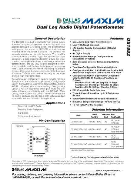
DS1882 Dual Log Audio Digital Potentiometer
DS1882 Dual Log Audio Digital Potentiometer
DS1882 Dual Log Audio Digital Potentiometer
- No tags were found...

You also want an ePaper? Increase the reach of your titles
YUMPU automatically turns print PDFs into web optimized ePapers that Google loves.
<strong>Dual</strong> <strong>Log</strong> <strong>Audio</strong> <strong>Digital</strong> <strong>Potentiometer</strong><br />
<strong>DS1882</strong><br />
Pin Description<br />
PIN NAME FUNCTION<br />
1 GND Ground<br />
2 A2<br />
I 2 C Address Inputs. Inputs A0, A1, and A2 determine the I 2 C slave address of the device.<br />
3 A1<br />
4 V- Negative Analog Voltage Supply<br />
5 A0 I 2 C Address Input. Inputs A0, A1, and A2 determine the I 2 C slave address of the device.<br />
6 W0 Wiper Terminal for <strong>Potentiometer</strong> 0<br />
7 L0 Low Terminal for <strong>Potentiometer</strong> 0<br />
8 H0 High Terminal for <strong>Potentiometer</strong> 0<br />
9 L1 Low Terminal for <strong>Potentiometer</strong> 1<br />
10 H1 High Terminal for <strong>Potentiometer</strong> 1<br />
11 W1 Wiper Terminal for <strong>Potentiometer</strong> 1<br />
12 CE Chip Enable. Enables SDA and SCL pins for I 2 C communication.<br />
13 SDA I 2 C Serial-Data Open-Drain I/O<br />
14 SCL I 2 C Serial-Clock Input<br />
15 V CC Analog Voltage Supply<br />
16 V DD <strong>Digital</strong> Voltage Supply<br />
Block Diagram<br />
SDA<br />
SCL<br />
A2<br />
A1<br />
A0<br />
CE<br />
I 2 C<br />
INTERFACE<br />
CONFIGURATION<br />
REGISTER<br />
POTENTIOMETER<br />
SETTING<br />
REGISTERS<br />
<strong>DS1882</strong><br />
V DD<br />
V-<br />
V CC<br />
GND<br />
V CC<br />
V DD<br />
GND<br />
V-<br />
POTENTIOMETER 0<br />
VALUE<br />
DECODER<br />
POTENTIOMETER 1<br />
VALUE<br />
H0<br />
H1<br />
W0<br />
W1<br />
L0<br />
ZERO-CROSSING<br />
DETECTOR<br />
ZERO-CROSSING<br />
DETECTOR<br />
L1<br />
UPDATE<br />
UPDATE<br />
6 _____________________________________________________________________
<strong>Dual</strong> <strong>Log</strong> <strong>Audio</strong> <strong>Digital</strong> <strong>Potentiometer</strong><br />
I 2 C Interface for the <strong>DS1882</strong><br />
The CE pin serves as a communication enable pin.<br />
When active (CE = 0), the inputs SDA and SCL are recognized<br />
by the device. If inactive (CE = 1), pins SDA<br />
and SCL are disabled, making I 2 C communication<br />
impossible.<br />
Three pins, A0, A1, A2, serve as slave address inputs.<br />
For multidrop configurations, they allow eight such<br />
devices to be addressed by the same I 2 C bus. If the<br />
I 2 C address matches the hardware levels of these bits,<br />
the <strong>DS1882</strong> is allowed to receive communications from<br />
the I 2 C bus.<br />
The I 2 C slave address byte is shown below. This is the<br />
first byte transmitted from the master to the <strong>DS1882</strong>.<br />
The upper nibble value is fixed to 0101. Bit values A2,<br />
A1, and A0 are determined by the states of the corresponding<br />
pins. The LSB, R/W, determines whether a<br />
read or write will be performed.<br />
The next byte to be transmitted is the Command Byte<br />
(see the Command Byte section for details).<br />
<strong>DS1882</strong><br />
SLAVE ADDRESS BYTE<br />
0 1 0 1 A2 A1 A0 R/W<br />
MSB<br />
LSB<br />
Reading Pot Values<br />
As shown in Figure 1, the <strong>DS1882</strong> provides one read<br />
command operation. This operation allows the user to<br />
read both <strong>Potentiometer</strong> Wiper Setting Registers and<br />
the Configuration Register. To initiate a read operation,<br />
the R/W bit of the slave address byte is set to 1.<br />
Communication to read the <strong>DS1882</strong> begins with a<br />
START condition, which is issued by the master device.<br />
The slave address byte sent from the master device follows<br />
the START condition. Once a matching slave<br />
address byte has been received by the <strong>DS1882</strong>, the<br />
<strong>DS1882</strong> responds with an acknowledge. The master<br />
can then begin to receive data. The value of the wiper<br />
of <strong>Potentiometer</strong> 0 is the first returned from the <strong>DS1882</strong>.<br />
It is then followed by the value of <strong>Potentiometer</strong> 1 and<br />
then the value of the Configuration Register. Once the 8<br />
bits of the Configuration Register have been sent, the<br />
master needs to issue an acknowledge, unless it is the<br />
last byte to be read, in which case the master issues a<br />
not acknowledge. If desired, the master may stop the<br />
communication transfer at this point by issuing the<br />
STOP condition after the not acknowledge. However, if<br />
the value of the three registers is needed again, the<br />
transfer can continue by clocking the 8 bits of the<br />
<strong>Potentiometer</strong> 0 value as described above.<br />
READ PROTOCOL<br />
MSB<br />
SLAVE ADDRESS<br />
BYTE<br />
LSB<br />
MSB<br />
COMMAND<br />
BYTE<br />
LSB<br />
MSB<br />
COMMAND<br />
BYTE<br />
LSB<br />
MSB<br />
COMMAND<br />
BYTE<br />
LSB<br />
START<br />
0<br />
1 0 1<br />
A<br />
2<br />
A<br />
1<br />
A<br />
0<br />
1<br />
ACK<br />
0<br />
0<br />
POT-0 0 1<br />
ACK<br />
POT-1<br />
ACK<br />
1 0<br />
CONFIG<br />
REG<br />
NACK<br />
STOP<br />
R/W = 1<br />
DATA BYTES ARE READ IN THE ORDER SHOWN ABOVE.<br />
Figure 1. Read Protocol<br />
____________________________________________________________________ 11
<strong>Dual</strong> <strong>Log</strong> <strong>Audio</strong> <strong>Digital</strong> <strong>Potentiometer</strong><br />
<strong>DS1882</strong><br />
Writing Command Byte Values<br />
An example of writing to the <strong>DS1882</strong> is shown in Figure 2.<br />
The <strong>DS1882</strong> has one write command that is used to<br />
change the <strong>Potentiometer</strong> Wiper Setting Registers and<br />
the Configuration Register. All write operations begin with<br />
a START from the master, followed by a slave address<br />
byte. The R/W bit should be written to 0, which initiates<br />
a write command. Once the slave address byte has<br />
been issued and the master receives the acknowledge<br />
from the <strong>DS1882</strong>, potentiometer wiper data is transmitted<br />
to the <strong>DS1882</strong> by the master device.<br />
If the potentiometer has been configured to be written<br />
in nonvolatile memory (see the Configuration Register<br />
section), then the acknowledge needs to be followed<br />
with a STOP command. This command is required from<br />
the master at the end of data transmission to initiate the<br />
EEPROM write. The STOP command is also accepted if<br />
the user has configured the pot values to be written in<br />
volatile memory, but no EEPROM is written to.<br />
I 2 C Serial Interface Description<br />
I 2 C interface supports a bidirectional data transmission<br />
protocol with device addressing. A device that sends<br />
data on the bus is defined as a transmitter, and a<br />
device receiving data as a receiver. The device that<br />
controls the message is called a master. The devices<br />
that are controlled by the master are slaves. The bus<br />
must be controlled by a master device that generates<br />
the serial clock (SCL), controls the bus access, and<br />
generates the START and STOP conditions. The<br />
<strong>DS1882</strong> operates as a slave on the I 2 C bus. Connections<br />
to the bus are made by the open-drain I/O lines, SDA<br />
and SCL. The following I/O terminals control the I 2 C<br />
serial port: CE, SDA, SCL, A0, A1, and A2. A data<br />
transfer protocol and a timing diagram are provided in<br />
Figures 3 and 4. The following terminology is commonly<br />
used to describe I 2 C data transfers.<br />
I 2 C Definitions<br />
Master Device: The master device controls the slave<br />
devices on the bus. The master device generates SCL<br />
clock pulses, START and STOP conditions.<br />
Slave Devices: Slave devices send and receive data<br />
at the master’s request.<br />
Bus Idle or Not Busy: Time between STOP and START<br />
conditions when both SDA and SCL are inactive and in<br />
their logic-high states. When the bus is idle it often initiates<br />
a low-power mode for slave devices.<br />
START Condition: A START condition is generated by<br />
the master to initiate a new data transfer with a slave.<br />
Transitioning SDA from high to low while SCL remains<br />
high generates a START condition. See the timing diagram<br />
for applicable timing.<br />
STOP Condition: A STOP condition is generated by<br />
the master to end a data transfer with a slave.<br />
Transitioning SDA from low to high while SCL remains<br />
high generates a STOP condition. See the timing diagram<br />
for applicable timing.<br />
Repeated START Condition: The master can use a<br />
repeated START condition at the end of one data transfer<br />
to indicate that it will immediately initiate a new data<br />
transfer following the current one. Repeated STARTs<br />
are commonly used during read operations to identify a<br />
specific memory address to begin a data transfer. A<br />
repeated START condition is issued identically to a normal<br />
START condition. See the timing diagram for<br />
applicable timing.<br />
Bit Write: Transitions of SDA must occur during the low<br />
state of SCL. The data on SDA must remain valid and<br />
unchanged during the entire high pulse of SCL plus the<br />
setup and hold-time requirements (see Figure 4). Data is<br />
shifted into the device during the rising edge of the SCL.<br />
Bit Read: At the end of a write operation, the master<br />
must release the SDA bus line for the proper amount of<br />
WRITE PROTOCOL<br />
MSB<br />
SLAVE ADDRESS<br />
BYTE<br />
LSB<br />
MSB<br />
COMMAND<br />
BYTE<br />
LSB<br />
MSB<br />
COMMAND<br />
BYTE<br />
LSB<br />
MSB<br />
COMMAND<br />
BYTE<br />
LSB<br />
START<br />
0<br />
1 0 1<br />
A<br />
2<br />
A<br />
1<br />
A<br />
0<br />
0<br />
ACK<br />
0<br />
0<br />
POT-0 0 1<br />
ACK<br />
POT-1<br />
ACK<br />
1 0<br />
CONFIG<br />
REG<br />
ACK<br />
STOP<br />
R/W = 0<br />
DATA BYTES CAN BE WRITTEN IN ANY ORDER.<br />
Figure 2. Write Protocol<br />
12 ____________________________________________________________________
<strong>Dual</strong> <strong>Log</strong> <strong>Audio</strong> <strong>Digital</strong> <strong>Potentiometer</strong><br />
setup time (see Figure 4) before the next rising edge of<br />
SCL during a bit read. The device shifts out each bit of<br />
data on SDA at the falling edge of the previous SCL<br />
pulse, and the data bit is valid at the rising edge of the<br />
current SCL pulse. Remember that the master generates<br />
all SCL clock pulses, including when it is reading<br />
bits from the slave.<br />
Acknowledgement (ACK and NACK): An Acknowledgement<br />
(ACK) or Not Acknowledge (NACK) is always the<br />
9th bit transmitted during a byte transfer. The device<br />
receiving data (the master during a read or the slave<br />
during a write operation) performs an ACK by transmitting<br />
a zero during the 9th bit. A device performs a<br />
NACK by transmitting a one during the 9th bit. Timing<br />
(Figure 4) for the ACK and NACK is identical to all other<br />
bit writes. An ACK is the acknowledgment that the<br />
device is properly receiving data. A NACK is used to<br />
terminate a read sequence or as an indication that the<br />
device is not receiving data.<br />
<strong>DS1882</strong><br />
SDA<br />
MSB<br />
SLAVE ADDRESS<br />
R/W<br />
DIRECTION<br />
BIT<br />
ACKNOWLEDGEMENT<br />
SIGNAL FROM RECEIVER<br />
ACKNOWLEDGEMENT<br />
SIGNAL FROM RECEIVER<br />
SCL<br />
1 2 6 7 8 9 1 2 3–7 8 9<br />
START<br />
CONDITION<br />
ACK<br />
REPEATED IF MORE BYTES<br />
ARE TRANSFERRED<br />
ACK<br />
STOP<br />
CONDITION<br />
OR REPEATED<br />
START<br />
CONDITION<br />
Figure 3. Data Transfer Protocol<br />
SDA<br />
t BUF<br />
t HD:STA<br />
t SP<br />
t LOW<br />
t R<br />
t F<br />
SCL<br />
t HD:STA<br />
t HIGH<br />
t SU:STA<br />
STOP<br />
START<br />
t SU:DAT REPEATED<br />
START<br />
t SU:STO<br />
NOTE: TIMING IS REFERENCED TO V IL(MAX) AND V IH(MIN) .<br />
Figure 4. I 2 C Timing Diagram<br />
____________________________________________________________________ 13
<strong>Dual</strong> <strong>Log</strong> <strong>Audio</strong> <strong>Digital</strong> <strong>Potentiometer</strong><br />
<strong>DS1882</strong><br />
Byte Write: A byte write consists of 8 bits of information<br />
transferred from the master to the slave (most significant<br />
bit first) plus a 1-bit acknowledgement from the<br />
slave to the master. The 8 bits transmitted by the master<br />
are done according to the bit write definition and the<br />
acknowledgement is read using the bit read definition.<br />
Byte Read: A byte read is an 8-bit information transfer<br />
from the slave to the master plus a 1-bit ACK or NACK<br />
from the master to the slave. The 8 bits of information<br />
that are transferred (most significant bit first) from the<br />
slave to the master are read by the master using the bit<br />
read definition, and the master transmits an ACK using<br />
the bit write definition to receive additional data bytes.<br />
The master must NACK the last byte read to terminate<br />
communication so the slave will return control of SDA to<br />
the master.<br />
Slave Address Byte: Each slave on the I 2 C bus<br />
responds to a slave addressing byte sent immediately<br />
following a START condition. The slave address byte<br />
(Figure 5) contains the slave address in the most significant<br />
7 bits and the R/W bit in the least significant bit.<br />
The <strong>DS1882</strong>’s slave address is 0101 A2 A1 A0 (binary),<br />
where A2, A1, and A0 are the values of the address<br />
pins. The address pins allow the device to respond to<br />
one of eight possible slave addresses. By writing the<br />
correct slave address with R/W = 0, the master indicates<br />
it will write data to the slave. If R/W = 1, the master<br />
will read data from the slave. If an incorrect slave<br />
address is written, the <strong>DS1882</strong> will assume the master is<br />
communicating with another I 2 C device and ignore the<br />
communications until the next START condition is sent.<br />
I 2 C Communication<br />
Writing a Single Byte to a Slave: The master must<br />
generate a START condition, write the slave address<br />
byte (R/W = 0), write the byte of data, and generate a<br />
STOP condition. The master must read the slave’s<br />
acknowledgement during all byte write operations.<br />
0<br />
MSB<br />
7-BIT SLAVE<br />
ADDRESS<br />
DETERMINES<br />
READ OR WRITE<br />
FUNCTION<br />
1 0 1 A2 A1 A0 R/W<br />
A2, A1, AND A0<br />
PIN VALUES<br />
Figure 5. <strong>DS1882</strong>’s Slave Address Byte<br />
LSB<br />
Writing Multiple Bytes to a Slave: To write multiple<br />
bytes to a slave, the master generates a START condition,<br />
writes the slave address byte (R/W = 0), writes the<br />
desired number of data bytes and generates a STOP<br />
condition. The <strong>DS1882</strong> is capable of writing both potentiometer<br />
wiper settings and the Configuration Register<br />
with a single write transaction.<br />
Acknowledge Polling: Any time an EEPROM location<br />
is written, the <strong>DS1882</strong> requires the EEPROM write time<br />
(t W ) after the STOP condition to write the contents of<br />
the byte of data to EEPROM. During the EEPROM write<br />
time, the device will not acknowledge its slave address<br />
because it is busy. It is possible to take advantage of<br />
that phenomenon by repeatedly addressing the<br />
<strong>DS1882</strong>, which allows the next page to be written as<br />
soon as the <strong>DS1882</strong> is ready to receive the data. The<br />
alternative to acknowledge polling is to wait for a maximum<br />
period of t W to elapse before attempting to write<br />
again to the device.<br />
EEPROM Write Cycles: When EEPROM writes occur to<br />
the memory, the <strong>DS1882</strong> will write to all three EEPROM<br />
memory locations, even if only a single byte was modified.<br />
Because all three bytes are written, the bytes that<br />
were not modified during the write transaction are still<br />
subject to a write cycle. This can result in all three bytes<br />
being worn out over time by writing a single byte repeatedly.<br />
The <strong>DS1882</strong>’s EEPROM write cycles are specified in<br />
the NV Memory Characteristics table. The specification<br />
shown is at the worst-case temperature. If zero-crossing<br />
detection is enabled, EEPROM write cycles cannot begin<br />
until after the zero-crossing detection is complete.<br />
Reading a Single Byte from a Slave: To read a single<br />
byte from the slave, the master generates a START condition,<br />
writes the slave address byte with R/W = 1, reads<br />
the data byte with a NACK to indicate the end of the<br />
transfer, and generates a STOP condition. When a single<br />
byte is read, it will always be the <strong>Potentiometer</strong> 0 value.<br />
Reading Multiple Bytes from a Slave: The read operation<br />
can be used to read multiple bytes with a single<br />
transfer. When reading bytes from the slave, the master<br />
simply ACKs the data byte if it desires to read another<br />
byte before terminating the transaction. After the master<br />
reads the last byte, it NACKs to indicate the end of<br />
the transfer and generates a STOP condition. The first<br />
byte read will be the <strong>Potentiometer</strong> 0 Wiper Setting. The<br />
next byte will be the <strong>Potentiometer</strong> 1 Wiper Setting. The<br />
third byte is the Configuration Register byte. If an ACK<br />
is issued by the master following the Configuration<br />
Register byte, then the <strong>DS1882</strong> will send the<br />
<strong>Potentiometer</strong> 0 Wiper Setting again. This round robin<br />
reading will occur as long as each byte read is followed<br />
by an ACK from the master.<br />
14 ____________________________________________________________________
<strong>Dual</strong> <strong>Log</strong> <strong>Audio</strong> <strong>Digital</strong> <strong>Potentiometer</strong><br />
Applications Information<br />
Power-Supply Decoupling<br />
To achieve best results, it is recommended that the<br />
power supplies are decoupled with a 0.01μF or a 0.1μF<br />
capacitor. Use high-quality, ceramic, surface-mount<br />
capacitors, and mount the capacitors as close as possible<br />
to the voltage supplies and GND pins to minimize<br />
lead inductance.<br />
SDA and SCL Pullup Resistors<br />
SDA is an open-collector output on the <strong>DS1882</strong> that<br />
requires a pullup resistor to realize high logic levels. A<br />
master using either an open-collector output with a<br />
pullup resistor or a push-pull output driver can be utilized<br />
for SCL. Pullup resistor values should be chosen<br />
to ensure that the rise and fall times listed in the AC<br />
Electrical Characteristics table are within specification.<br />
<strong>DS1882</strong><br />
Typical Operating Circuit<br />
5V (V DD )<br />
5V (V CC )<br />
4.7kΩ<br />
4.7kΩ<br />
DECOUPLING<br />
CAPACITOR<br />
V DD<br />
GND<br />
V CC<br />
DECOUPLING<br />
CAPACITOR<br />
SDA<br />
HOST<br />
μC<br />
SCL<br />
CE<br />
<strong>DS1882</strong><br />
H1<br />
W1<br />
A2<br />
L1<br />
A1<br />
A0<br />
H0<br />
W0<br />
AUDIO<br />
OUT<br />
-5V (V-)<br />
V-<br />
L0<br />
DECOUPLING<br />
CAPACITOR<br />
AUDIO IN<br />
TRANSISTOR COUNT: 52,353<br />
SUBSTRATE CONNECTED TO GROUND<br />
Chip Topology<br />
Package Information<br />
For the latest package outline information, go to<br />
www.maxim-ic.com/DallasPackInfo.<br />
Maxim cannot assume responsibility for use of any circuitry other than circuitry entirely embodied in a Maxim product. No circuit patent licenses are<br />
implied. Maxim reserves the right to change the circuitry and specifications without notice at any time.<br />
Maxim Integrated Products, 120 San Gabriel Drive, Sunnyvale, CA 94086 408-737-7600 ____________________ 15<br />
© 2006 Maxim Integrated Products is a registered trademark of Maxim Integrated Products, Inc.<br />
Springer<br />
is a registered trademark of Dallas Semiconductor Corporation.


