ICM205B VGA/QVGA CMOS image sensor with digital YUV output ...
ICM205B VGA/QVGA CMOS image sensor with digital YUV output ...
ICM205B VGA/QVGA CMOS image sensor with digital YUV output ...

Create successful ePaper yourself
Turn your PDF publications into a flip-book with our unique Google optimized e-Paper software.
Functional Description<br />
Image Array<br />
<strong>ICM205B</strong>: <strong>VGA</strong> <strong>CMOS</strong> <strong>sensor</strong> <strong>with</strong> <strong>digital</strong> <strong>YUV</strong> <strong>output</strong><br />
Engineering Specification V1.1, July. 2002<br />
The <strong>image</strong> array consists of 640x480 pixels. Each pixel has a light sensitive photo diode and a set of<br />
control and transfer transistors. At the beginning of the cycle, a row of pixels are pre-charged to its<br />
maximum value. Then they are exposed to light for several lines worth of time and sampled by the ADC.<br />
Correlated double sampling (CDS) is performed by subtracting the reset value (sampled right before<br />
sampling the signal) from the signal value. The purpose of CDS is to eliminate the point-wise fixed<br />
pattern noise (FPN). The <strong>output</strong> of CDS is approximately proportional to the amount of received light,<br />
ranging from 0 to 255.<br />
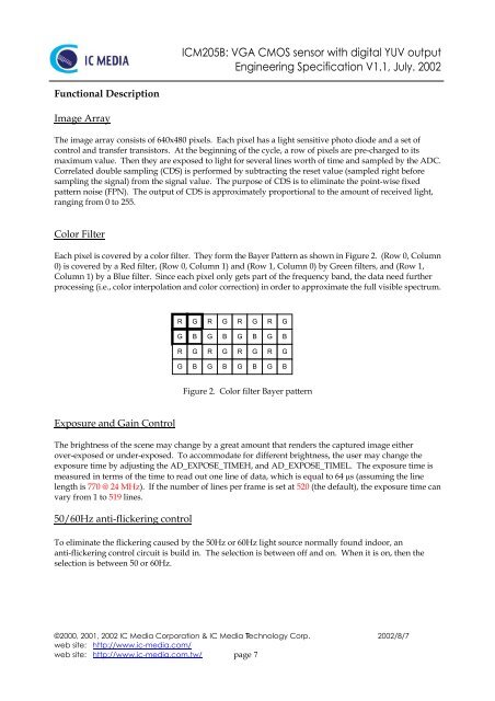
Color Filter<br />
Each pixel is covered by a color filter. They form the Bayer Pattern as shown in Figure 2. (Row 0, Column<br />
0) is covered by a Red filter, (Row 0, Column 1) and (Row 1, Column 0) by Green filters, and (Row 1,<br />
Column 1) by a Blue filter. Since each pixel only gets part of the frequency band, the data need further<br />
processing (i.e., color interpolation and color correction) in order to approximate the full visible spectrum.<br />
Exposure and Gain Control<br />
R G R G R G R G<br />
G B G B G B G B<br />
R G R G R G R G<br />
G B G B G B G B<br />
Figure 2. Color filter Bayer pattern<br />
The brightness of the scene may change by a great amount that renders the captured <strong>image</strong> either<br />
over-exposed or under-exposed. To accommodate for different brightness, the user may change the<br />
exposure time by adjusting the AD_EXPOSE_TIMEH, and AD_EXPOSE_TIMEL. The exposure time is<br />
measured in terms of the time to read out one line of data, which is equal to 64 µs (assuming the line<br />
length is 770 @ 24 MHz). If the number of lines per frame is set at 520 (the default), the exposure time can<br />
vary from 1 to 519 lines.<br />
50/60Hz anti-flickering control<br />
To eliminate the flickering caused by the 50Hz or 60Hz light source normally found indoor, an<br />
anti-flickering control circuit is build in. The selection is between off and on. When it is on, then the<br />
selection is between 50 or 60Hz.<br />
©2000, 2001, 2002 IC Media Corporation & IC Media Technology 7<br />
Corp. 2002/8/7<br />
web site: http://www.ic-media.com/<br />
web site: http://www.ic-media.com.tw/ page 7