Using uM-FPU V3.1 with the PICBASIC PRO Compiler
Using uM-FPU V3.1 with the PICBASIC PRO compiler - Micromega
Using uM-FPU V3.1 with the PICBASIC PRO compiler - Micromega
- No tags were found...

You also want an ePaper? Increase the reach of your titles
YUMPU automatically turns print PDFs into web optimized ePapers that Google loves.
<strong>Using</strong> <strong>uM</strong>-<strong>FPU</strong> <strong>V3.1</strong><br />
<strong>with</strong> <strong>the</strong> <strong>PICBASIC</strong> <strong>PRO</strong><br />
<strong>Compiler</strong><br />
Introduction<br />
The <strong>uM</strong>-<strong>FPU</strong> <strong>V3.1</strong> chip is a 32-bit floating point coprocessor that can be easily interfaced <strong>with</strong> Microchip<br />
Technology PIC® microcontrollers, and programmed using <strong>the</strong> <strong>PICBASIC</strong> <strong>PRO</strong> <strong>Compiler</strong> from<br />
microEngineering Labs, to provide support for 32-bit IEEE 754 floating point operations and 32-bit long integer<br />
operations. The <strong>uM</strong>-<strong>FPU</strong> <strong>V3.1</strong> chip supports both I 2 C and SPI connections.<br />
This document describes how to use <strong>the</strong> <strong>uM</strong>-<strong>FPU</strong> <strong>V3.1</strong> chip <strong>with</strong> <strong>the</strong> <strong>PICBASIC</strong> <strong>PRO</strong> <strong>Compiler</strong>. For a full<br />
description of <strong>the</strong> <strong>uM</strong>-<strong>FPU</strong> <strong>V3.1</strong> chip, please refer to <strong>the</strong> <strong>uM</strong>-<strong>FPU</strong> <strong>V3.1</strong> Datasheet and <strong>uM</strong>-<strong>FPU</strong> <strong>V3.1</strong> Instruction<br />
Reference. Application notes are also available on <strong>the</strong> Micromega website.<br />
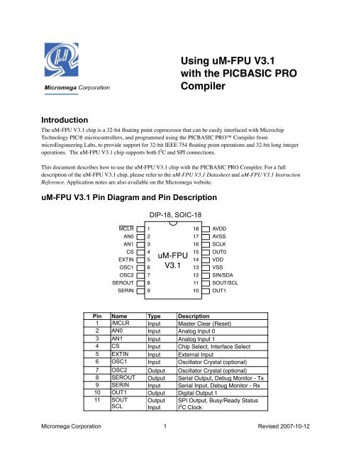
<strong>uM</strong>-<strong>FPU</strong> <strong>V3.1</strong> Pin Diagram and Pin Description<br />
DIP-18, SOIC-18<br />
MCLR<br />
1<br />
18<br />
AVDD<br />
AN0<br />
2<br />
17<br />
AVSS<br />
AN1<br />
3<br />
16<br />
SCLK<br />
CS<br />
EXTIN<br />
OSC1<br />
4<br />
5<br />
6<br />
<strong>uM</strong>-<strong>FPU</strong><br />
<strong>V3.1</strong><br />
15<br />
14<br />
13<br />
OUT0<br />
VDD<br />
VSS<br />
OSC2<br />
7<br />
12<br />
SIN/SDA<br />
SEROUT<br />
8<br />
11<br />
SOUT/SCL<br />
SERIN<br />
9<br />
10<br />
OUT1<br />
Pin<br />
1<br />
2<br />
3<br />
4<br />
5<br />
6<br />
7<br />
8<br />
9<br />
10<br />
11<br />
Name<br />
/MCLR<br />
AN0<br />
AN1<br />
CS<br />
EXTIN<br />
OSC1<br />
OSC2<br />
SEROUT<br />
SERIN<br />
OUT1<br />
SOUT<br />
SCL<br />
Type<br />
Input<br />
Input<br />
Input<br />
Input<br />
Input<br />
Input<br />
Output<br />
Output<br />
Input<br />
Output<br />
Output<br />
Input<br />
Description<br />
Master Clear (Reset)<br />
Analog Input 0<br />
Analog Input 1<br />
Chip Select, Interface Select<br />
External Input<br />
Oscillator Crystal (optional)<br />
Oscillator Crystal (optional)<br />
Serial Output, Debug Monitor - Tx<br />
Serial Input, Debug Monitor - Rx<br />
Digital Output 1<br />
SPI Output, Busy/Ready Status<br />
I 2 C Clock<br />
Micromega Corporation 1 Revised 2007-10-12
12<br />
13<br />
14<br />
15<br />
16<br />
17<br />
18<br />
SIN<br />
SDA<br />
VSS<br />
VDD<br />
OUT0<br />
SCLK<br />
AVSS<br />
AVDD<br />
Input<br />
In/Out<br />
Power<br />
Power<br />
Output<br />
Input<br />
Power<br />
Power<br />
SPI Input<br />
I 2 C Data<br />
Digital Ground<br />
Digital Supply Voltage<br />
Digital Output 0<br />
SPI Clock<br />
Analog Ground<br />
Analog Supply Voltage<br />
Connecting <strong>the</strong> Microchip PIC using 2-wire SPI<br />
Only two pins are required for interfacing a Microchip PIC to <strong>the</strong> <strong>uM</strong>-<strong>FPU</strong> <strong>V3.1</strong> chip using a 2-wire SPI interface.<br />
The communication uses a bidirectional serial interface that requires a clock pin and a data pin. An example of <strong>the</strong><br />
pin settings for a Microchip PIC are shown below. (They can be changed to suit your application.)<br />
FpuClk var PORTC.3 ' pin RC3<br />
FpuIn var PORTC.4 ' pin RC4<br />
FpuOut var PORTC.4 ' pin RC4<br />
Microchip PIC Pins<br />
FpuOut/FpuIn<br />
FpuClk<br />
VDD<br />
<strong>uM</strong>-<strong>FPU</strong> <strong>V3.1</strong><br />
VDD<br />
1<br />
2<br />
3<br />
4<br />
5<br />
6<br />
7<br />
8<br />
9<br />
/MCLR<br />
AN0<br />
AN1<br />
CS<br />
EXTIN<br />
OSC1<br />
OSC2<br />
SEROUT<br />
SERIN<br />
18<br />
AVDD<br />
17<br />
AVSS<br />
16<br />
SCLK<br />
15<br />
OUT0<br />
14<br />
VDD<br />
13<br />
VSS<br />
12<br />
SIN/SDA<br />
11<br />
SOUT/SCL<br />
10<br />
OUT1<br />
1K<br />
Connecting <strong>the</strong> Microchip PIC using 3-wire SPI<br />
Three pins are required for interfacing a Microchip PIC to <strong>the</strong> <strong>uM</strong>-<strong>FPU</strong> <strong>V3.1</strong> chip using a 3-wire SPI interface. The<br />
communication uses a clock pin, an input data pin, and an output data pin. An example of <strong>the</strong> pin settings for a<br />
Microchip PIC are shown below. (They can be changed to suit your application.)<br />
FpuClk var PORTC.3 ' pin RC3<br />
FpuIn var PORTC.4 ' pin RC4<br />
FpuOut var PORTC.5 ' pin RC5<br />
Micromega Corporation 2 <strong>uM</strong>-<strong>FPU</strong> <strong>V3.1</strong> and <strong>the</strong> <strong>PICBASIC</strong> <strong>PRO</strong> <strong>Compiler</strong>
Microchip PIC Pins<br />
FpuIn<br />
FpuOut<br />
FpuClk<br />
VDD<br />
<strong>uM</strong>-<strong>FPU</strong> <strong>V3.1</strong><br />
VDD<br />
1<br />
2<br />
3<br />
4<br />
5<br />
6<br />
7<br />
8<br />
9<br />
/MCLR<br />
AN0<br />
AN1<br />
CS<br />
EXTIN<br />
OSC1<br />
OSC2<br />
SEROUT<br />
SERIN<br />
18<br />
AVDD<br />
17<br />
AVSS<br />
16<br />
SCLK<br />
15<br />
OUT0<br />
14<br />
VDD<br />
13<br />
VSS<br />
12<br />
SIN/SDA<br />
11<br />
SOUT/SCL<br />
10<br />
OUT1<br />
Connecting <strong>the</strong> Microchip PIC using I 2 C<br />
The <strong>uM</strong>-<strong>FPU</strong> <strong>V3.1</strong> can also be connected using an I 2 C interface. The default slave ID for <strong>the</strong> <strong>uM</strong>-<strong>FPU</strong> chip is $C8.<br />
An example of <strong>the</strong> pin settings for a Microchip PIC are shown below (<strong>the</strong>y can be changed to suit your application):<br />
Fpu_SCL var PORTC.3 ' pin RC3<br />
Fpu_SDA var PORTC.4 ' pin RC4<br />
Fpu_ID con $C8 ' <strong>uM</strong>-<strong>FPU</strong> I2C device address<br />
VDD<br />
Microchip PIC Pins<br />
SCL<br />
SDA<br />
4.7K<br />
4.7K<br />
Note: SCL and SDA<br />
must have pull-up<br />
resistors as required<br />
by <strong>the</strong> I2C bus.<br />
VDD<br />
1<br />
2<br />
3<br />
4<br />
5<br />
6<br />
7<br />
8<br />
9<br />
<strong>uM</strong>-<strong>FPU</strong> <strong>V3.1</strong><br />
/MCLR<br />
AN0<br />
AN1<br />
CS<br />
EXTIN<br />
OSC1<br />
OSC2<br />
SEROUT<br />
SERIN<br />
18<br />
AVDD<br />
17<br />
AVSS<br />
16<br />
SCLK<br />
15<br />
OUT0<br />
14<br />
VDD<br />
13<br />
VSS<br />
12<br />
SIN/SDA<br />
11<br />
SOUT/SCL<br />
10<br />
OUT1<br />
VDD<br />
Micromega Corporation 3 <strong>uM</strong>-<strong>FPU</strong> <strong>V3.1</strong> and <strong>the</strong> <strong>PICBASIC</strong> <strong>PRO</strong> <strong>Compiler</strong>
Brief Overview of <strong>the</strong> <strong>uM</strong>-<strong>FPU</strong> <strong>V3.1</strong> Floating Point Coprocessor<br />
For a full description of <strong>the</strong> <strong>uM</strong>-<strong>FPU</strong> <strong>V3.1</strong> chip, please refer to <strong>the</strong> <strong>uM</strong>-<strong>FPU</strong> <strong>V3.1</strong> Datasheet, <strong>uM</strong>-<strong>FPU</strong> <strong>V3.1</strong><br />
Instruction Reference. Application notes are also available on <strong>the</strong> Micromega website.<br />
The <strong>uM</strong>-<strong>FPU</strong> <strong>V3.1</strong> chip is a separate coprocessor <strong>with</strong> its own set of registers and instructions designed to provide<br />
microcontrollers <strong>with</strong> 32-bit floating point and long integer capabilities. The Microchip PIC communicates <strong>with</strong> <strong>the</strong><br />
<strong>FPU</strong> using an SPI or I 2 C interface. Instructions and data are sent to <strong>the</strong> <strong>FPU</strong>, and <strong>the</strong> <strong>FPU</strong> performs <strong>the</strong> calculations.<br />
The Microchip PIC is free to do o<strong>the</strong>r tasks while <strong>the</strong> <strong>FPU</strong> performs calculations. Results can be read back to <strong>the</strong><br />
Microchip PIC or stored on <strong>the</strong> <strong>FPU</strong> for later use. The <strong>uM</strong>-<strong>FPU</strong> <strong>V3.1</strong> chip has 128 registers, numbered 0 through<br />
127, that can hold 32-bit floating point or long integer values. Register 0 is often used as a temporary register and is<br />
modified by some of <strong>the</strong> <strong>uM</strong>-<strong>FPU</strong> <strong>V3.1</strong> instructions. Registers 1 through 127 are available for general use.<br />
The SELECTA instruction is used to select any one of <strong>the</strong> 128 registers as register A. Register A can be regarded as<br />
an accumulator or working register. Arithmetic instructions use <strong>the</strong> value in register A as an operand and store <strong>the</strong><br />
result of <strong>the</strong> operation in register A. If an instruction requires more than one operand, <strong>the</strong> additional operand is<br />
specified by <strong>the</strong> instruction. The following example selects register 2 as register A and adds register 5 to it:<br />
SELECTA, 2<br />
FADD, 5<br />
select register 2 as register A<br />
register[A] = register[A] + register[5]<br />
Sending Instructions to <strong>the</strong> <strong>uM</strong>-<strong>FPU</strong><br />
Appendix A contains a table that gives a summary of each <strong>uM</strong>-<strong>FPU</strong> <strong>V3.1</strong> instruction, <strong>with</strong> enough information to<br />
follow <strong>the</strong> examples in this document. For a detailed description of each instruction, refer to <strong>the</strong> <strong>uM</strong>-<strong>FPU</strong> <strong>V3.1</strong><br />
Instruction Reference.<br />
To send instructions to <strong>the</strong> <strong>FPU</strong> using a SPI interface, <strong>the</strong> SHIFTOUT command is used as follows:<br />
SHIFTOUT FpuOut, FpuClk, MSBFIRST, [FADD, 5]<br />
To send instructions to <strong>the</strong> <strong>FPU</strong> using an I 2 C interface, <strong>the</strong> I2CWRITE command is used as follows:<br />
I2CWRITE Fpu_SDA, Fpu_SCL, Fpu_ID, 0, [FADD, 5]<br />
The instructions and data to send to <strong>the</strong> <strong>FPU</strong> are located inside <strong>the</strong> square brackets. The beginning of <strong>the</strong> command<br />
is always <strong>the</strong> same, and depends on whe<strong>the</strong>r you are using an SPI or I 2 C interface. It tells <strong>the</strong> Microchip PIC how to<br />
communicate <strong>with</strong> <strong>the</strong> <strong>FPU</strong>. The SHIFTOUT command is used for <strong>the</strong> examples in this document, but <strong>the</strong><br />
I2CWRITE command would be substituted if an I 2 C interface is used.<br />
All instructions have an opcode that tells <strong>the</strong> <strong>FPU</strong> which operation to perform, The following example calculates <strong>the</strong><br />
square root of register A:<br />
SHIFTOUT FpuOut, FpuClk, MSBFIRST, [SQRT]<br />
Some instructions require additional operands or data and are specified by <strong>the</strong> bytes following <strong>the</strong> opcode. The<br />
following example adds register 5 to register A.<br />
SHIFTOUT FpuOut, FpuClk, MSBFIRST, [FADD, 5]<br />
Some instructions return data. This example reads <strong>the</strong> lower 8 bits of register A:<br />
Micromega Corporation 4 <strong>uM</strong>-<strong>FPU</strong> <strong>V3.1</strong> and <strong>the</strong> <strong>PICBASIC</strong> <strong>PRO</strong> <strong>Compiler</strong>
GOSUB Fpu_Wait<br />
SHIFTOUT FpuOut, FpuClk, MSBFIRST, [LREADBYTE]<br />
GOSUB Fpu_ReadDelay<br />
SHIFTIN FpuOut, FpuClk, MSBPRE, [dataByte]<br />
The following example adds <strong>the</strong> value in register 5 to <strong>the</strong> value in register 2.<br />
SHIFTOUT FpuOut, FpuClk, MSBFIRST, [SELECTA, 2, FADD, 5]<br />
It’s a good idea to use constant definitions to provide meaningful names for <strong>the</strong> registers. This makes your program<br />
easier to read and understand. The same example using constant definitions would be:<br />
Total CON 2 ' total amount (<strong>uM</strong>-<strong>FPU</strong> register)<br />
Count CON 5 ' current count (<strong>uM</strong>-<strong>FPU</strong> register)<br />
SHIFTOUT FpuOut, FpuClk, MSBFIRST, [SELECTA, Total, FADD, Count]<br />
Micromega Corporation 5 <strong>uM</strong>-<strong>FPU</strong> <strong>V3.1</strong> and <strong>the</strong> <strong>PICBASIC</strong> <strong>PRO</strong> <strong>Compiler</strong>
Tutorial Examples<br />
Now that we’ve introduced some of <strong>the</strong> basic concepts of sending instructions to <strong>the</strong> <strong>uM</strong>-<strong>FPU</strong> chip, let’s go through<br />
a tutorial example to get a better understanding of how it all ties toge<strong>the</strong>r. This example takes a temperature reading<br />
from a DS1620 digital <strong>the</strong>rmometer and converts it to Celsius and Fahrenheit.<br />
Most of <strong>the</strong> data read from devices connected to <strong>the</strong> Microchip PIC will return some type of integer value. In this<br />
example, <strong>the</strong> interface routine for <strong>the</strong> DS1620 reads a 9-bit value and stores it in a variable on <strong>the</strong> Microchip PIC<br />
called rawTemp. The value returned by <strong>the</strong> DS1620 is <strong>the</strong> temperature in units of 1/2 degrees Celsius. The<br />
following instructions load <strong>the</strong> rawTemp value to <strong>the</strong> <strong>FPU</strong>, convert it to floating point, <strong>the</strong>n divide it by 2 to get<br />
degrees in Celsius.<br />
SHIFTOUT FpuOut, FpuClk, MSBFIRST,<br />
[SELECTA, DegC, LOADWORD, rawTemp>>8, rawTemp, FSET0, FDIVI, 2]<br />
Description:<br />
SELECTA, DegC<br />
select DegC as register A<br />
LOADWORD, rawTemp>>8, rawTemp load rawTemp to register 0 and convert to floating point<br />
FSET0<br />
DegC = register[0] (i.e. <strong>the</strong> floating point value of rawTemp)<br />
FDIVI, 2 divide by <strong>the</strong> floating point value 2.0<br />
To get <strong>the</strong> degrees in Fahrenheit we use <strong>the</strong> formula F = C * 1.8 + 32. Since 1.8 is a constant value, it would<br />
normally be loaded once in <strong>the</strong> initialization section of <strong>the</strong> program and used later in <strong>the</strong> main program. The value<br />
1.8 can be loaded using <strong>the</strong> ATOF (ASCII to float) instruction as follows:<br />
SHIFTOUT FpuOut, FpuClk, MSBFIRST, [SELECTA, F1_8, ATOF, "1.8", 0, FSET0]<br />
Description:<br />
SELECTA, F1.8<br />
select F1_8 as register A<br />
ATOF, "1.8", 0<br />
load <strong>the</strong> string 1.8 (note: <strong>the</strong> string must be zero terminated),<br />
convert <strong>the</strong> string to floating point, and store in register 0<br />
FSET0 F1_8 = register[0] (i.e. 1.8)<br />
We calculate <strong>the</strong> degrees in Fahrenheit (F = C * 1.8 + 32) as follows:<br />
SHIFTOUT FpuOut, FpuClk, MSBFIRST,<br />
[SELECTA, DegF, FSET, DegC, FMUL, F1_8, FADDI, 32]<br />
Description:<br />
SELECTA, DegF<br />
select DegF as register A<br />
FSET, DegC<br />
DegF = DegC<br />
FMUL, F1_8 DegF = DegF * 1.8<br />
FADDI, 32 DegF = DegF + 32.0<br />
Note: this tutorial example is intended to show how to perform a familiar calculation, but <strong>the</strong> FCNV instruction<br />
could be used to perform unit conversions in one step. See <strong>the</strong> <strong>uM</strong>-<strong>FPU</strong> <strong>V3.1</strong> Instruction Reference for a full list of<br />
conversions.<br />
There are support routines provided for sending floating point and long integer strings to <strong>the</strong> debug port.<br />
Print_Float sends an unformatted floating point string and displays up to eight digits of precision.<br />
Print_FloatFormat sends a formatted floating point string. We’ll use Print_FloatFormat to send <strong>the</strong><br />
results to <strong>the</strong> debug port. The format variable is used to select <strong>the</strong> desired format, <strong>with</strong> <strong>the</strong> tens digit specifying<br />
<strong>the</strong> total number of characters to display, and <strong>the</strong> ones digit specifying <strong>the</strong> number of digits after <strong>the</strong> decimal point.<br />
Micromega Corporation 6 <strong>uM</strong>-<strong>FPU</strong> <strong>V3.1</strong> and <strong>the</strong> <strong>PICBASIC</strong> <strong>PRO</strong> <strong>Compiler</strong>
The DS1620 has a maximum temperature of 125° Celsius and one decimal point of precision, so we’ll use a format<br />
of 51. Before calling <strong>the</strong> Print_FloatFormat routine <strong>the</strong> <strong>FPU</strong> register is selected and <strong>the</strong> format variable is<br />
set. The following example sends <strong>the</strong> temperature in degrees Celsius and Fahrenheit to <strong>the</strong> debug port.<br />
SHIFTOUT FpuOut, FpuClk, MSBFIRST, [SELECTA, DegC]<br />
format = 51<br />
GOSUB Print_FloatFormat<br />
SHIFTOUT FpuOut, FpuClk, MSBFIRST, [SELECTA, DegF]<br />
format = 51<br />
GOSUB Print_FloatFormat<br />
Sample code for this tutorial and a wiring diagram for <strong>the</strong> DS1620 are shown at <strong>the</strong> end of this document. The file<br />
demo1.bas is also included <strong>with</strong> <strong>the</strong> support software. There is a second file called demo2.bas that extends this demo<br />
to include minimum and maximum temperature calculations. If you have a DS1620 you can wire up <strong>the</strong> circuit and<br />
try out <strong>the</strong> demos.<br />
Micromega Corporation 7 <strong>uM</strong>-<strong>FPU</strong> <strong>V3.1</strong> and <strong>the</strong> <strong>PICBASIC</strong> <strong>PRO</strong> <strong>Compiler</strong>
<strong>uM</strong>-<strong>FPU</strong> <strong>V3.1</strong> Support Software<br />
Support routines and opcode definitions for <strong>uM</strong>-<strong>FPU</strong> <strong>V3.1</strong> are contained in two include files: umfpuV3-spi.bas (for<br />
SPI connections), and umfpuV3-i2c.bas (for I 2 C connections) . To add <strong>uM</strong>-<strong>FPU</strong> <strong>V3.1</strong> support to a <strong>PICBASIC</strong> <strong>PRO</strong><br />
program, <strong>the</strong> main program should:<br />
• define <strong>the</strong> oscillator speed<br />
• define <strong>the</strong> debug port<br />
• define <strong>the</strong> <strong>uM</strong>-<strong>FPU</strong> <strong>V3.1</strong> pins<br />
• include <strong>the</strong> SPI or I 2 C support routines<br />
Sample code for an SPI interface is as follows:<br />
'-------------------- PIC oscillator speed ------------------------------------<br />
define OSC 20 ' specify <strong>the</strong> speed of <strong>the</strong> oscillator<br />
OSC_SPEED con 20 ' define <strong>PICBASIC</strong> constant<br />
'-------------------- debug definitions ---------------------------------------<br />
define DEBUG_REG PORTC<br />
define DEBUG_BIT 6<br />
defin DEBUG_BAUD 19200<br />
define DEBUG_MODE 0<br />
'-------------------- <strong>uM</strong>-<strong>FPU</strong> pin definitions ----------------------------------<br />
FpuClk var PORTC.3 ' SPI SCLK (<strong>uM</strong>-<strong>FPU</strong> SCLK)<br />
FpuIn var PORTC.4 ' SPI MISO (<strong>uM</strong>-<strong>FPU</strong> SOUT)<br />
FpuOut var PORTC.5 ' SPI MOSI (<strong>uM</strong>-<strong>FPU</strong> SIN)<br />
include "umfpuV3-spi.bas" ' include <strong>the</strong> <strong>uM</strong>-<strong>FPU</strong> V3 support routines<br />
Sample code for an I 2 C interface is as follows:<br />
'-------------------- PIC oscillator speed ------------------------------------<br />
define OSC 20 ' specify <strong>the</strong> speed of <strong>the</strong> oscillator<br />
OSC_SPEED con 20 ' define <strong>PICBASIC</strong> constant<br />
'-------------------- debug definitions ---------------------------------------<br />
define DEBUG_REG PORTC<br />
define DEBUG_BIT 6<br />
defin DEBUG_BAUD 19200<br />
define DEBUG_MODE 0<br />
'-------------------- <strong>uM</strong>-<strong>FPU</strong> pin definitions ----------------------------------<br />
Fpu_SCL var PORTC.3 ' I2C SCL pin (<strong>uM</strong>-<strong>FPU</strong> SCL)<br />
Fpu_SDA var PORTC.4 ' I2C SDA pin (<strong>uM</strong>-<strong>FPU</strong> SDA)<br />
Fpu_ID con $C8 ' <strong>uM</strong>-<strong>FPU</strong> I2C device address<br />
define I2C_HOLD 1 ' required for correct I2C timing<br />
include "umfpuV3-i2c.bas" ' include <strong>the</strong> <strong>uM</strong>-<strong>FPU</strong> V3 support routines<br />
The include files contain all of <strong>the</strong> support routines described below. Program template files (called template-spi.bas<br />
and template-i2c.bas) and various sample programs are provided for both SPI and I 2 C.<br />
Micromega Corporation 8 <strong>uM</strong>-<strong>FPU</strong> <strong>V3.1</strong> and <strong>the</strong> <strong>PICBASIC</strong> <strong>PRO</strong> <strong>Compiler</strong>
Fpu_Reset<br />
To ensure that <strong>the</strong> Microchip PIC and <strong>the</strong> <strong>FPU</strong> are synchronized, a reset call must be done at <strong>the</strong> start of every<br />
program. The Fpu_Reset routine resets <strong>the</strong> <strong>FPU</strong>, confirms communications, and returns <strong>the</strong> sync character ($5C)<br />
in <strong>the</strong> fpu_status variable if <strong>the</strong> reset is successful. A sample reset call is included in <strong>the</strong> template-spi.bas and<br />
template-i2c.bas files.<br />
Fpu_Wait<br />
The <strong>FPU</strong> must have completed all instructions in <strong>the</strong> instruction buffer, and be ready to return data, before sending<br />
an instruction to read data from <strong>the</strong> <strong>FPU</strong>. The Fpu_Wait routine checks <strong>the</strong> ready status of <strong>the</strong> <strong>FPU</strong> and waits until<br />
it is ready. The print routines check <strong>the</strong> ready status, so calling Fpu_Wait before calling a print routine isn’t<br />
required, but if your program reads directly from <strong>the</strong> <strong>FPU</strong> using <strong>the</strong> SHIFTIN or I2CREAD commands, a call to<br />
Fpu_Wait must be made prior to sending <strong>the</strong> read instruction. An example of reading a byte value is as follows:<br />
GOSUB Fpu_wait<br />
SHIFTOUT FpuOut, FpuClk, MSBFIRST, [LREADBYTE]<br />
GOSUB Fpu_ReadDelay<br />
SHIFTIN FpuOut, FpuClk, MSBPRE, [dataByte]<br />
Description:<br />
• wait for <strong>the</strong> <strong>FPU</strong> to be ready<br />
• send <strong>the</strong> LREADBYTE instruction<br />
• read a byte value and store it in <strong>the</strong> variable dataByte<br />
The <strong>uM</strong>-<strong>FPU</strong> <strong>V3.1</strong> chip has a 256 byte instruction buffer. In most cases, data will be read back before 256 bytes<br />
have been sent to <strong>the</strong> <strong>FPU</strong>. If a long calculation is done that requires more than 256 bytes to be sent to <strong>the</strong> <strong>FPU</strong>, an<br />
Fpu_Wait call should be made at least every 256 bytes to ensure that <strong>the</strong> instruction buffer doesn’t overflow.<br />
Fpu_ReadStatus<br />
The current status byte is read from <strong>the</strong> <strong>FPU</strong> and returned in <strong>the</strong> fpu_status variable.<br />
Fpu_ReadDelay<br />
After a read instruction is sent, and before <strong>the</strong> first data is read, a setup delay is required to ensure that <strong>the</strong> <strong>FPU</strong> is<br />
ready to send data. The Fpu_ReadDelay routine provides <strong>the</strong> required read setup delay. The delay is only<br />
required before <strong>the</strong> first byte read after a read instruction.<br />
Print_Version<br />
The <strong>FPU</strong> version string is sent to <strong>the</strong> debug port using <strong>the</strong> DEBUG command.<br />
Print_Float<br />
The value in register A is sent to <strong>the</strong> debug port as a floating point string using <strong>the</strong> DEBUG command. Up to eight<br />
significant digits will be displayed if required. Very large or very small numbers are displayed in exponential<br />
notation. The length of <strong>the</strong> displayed value is variable and can be from 3 to 12 characters in length. The special cases<br />
of NaN (Not a Number), +Infinity, -Infinity, and -0.0 are handled. Examples of <strong>the</strong> display format are as follows:<br />
1.0 NaN 0.0<br />
1.5e20 Infinity -0.0<br />
3.1415927 -Infinity 1.0<br />
-52.333334 -3.5e-5 0.01<br />
Print_FloatFormat<br />
The value in register A is sent to <strong>the</strong> debug port as a formatted floating point string using <strong>the</strong> DEBUG command. The<br />
Micromega Corporation 9 <strong>uM</strong>-<strong>FPU</strong> <strong>V3.1</strong> and <strong>the</strong> <strong>PICBASIC</strong> <strong>PRO</strong> <strong>Compiler</strong>
format variable is used to specify <strong>the</strong> desired format. The tens digit specifies <strong>the</strong> total number of characters to<br />
display and <strong>the</strong> ones digit specifies <strong>the</strong> number of digits after <strong>the</strong> decimal point. If <strong>the</strong> value is too large for <strong>the</strong><br />
format specified, <strong>the</strong>n asterisks will be displayed. If <strong>the</strong> number of digits after <strong>the</strong> decimal points is zero, no decimal<br />
point will be displayed. Examples of <strong>the</strong> display format are as follows:<br />
Value in A register format Display format<br />
123.567 61 (6.1) 123.6<br />
123.567 62 (6.2) 123.57<br />
123.567 42 (4.2) *.**<br />
0.9999 20 (2.0) 1<br />
0.9999 31 (3.1) 1.0<br />
Print_Long<br />
The value in register A is sent to <strong>the</strong> debug port as a signed long integer string using <strong>the</strong> DEBUG command. The<br />
displayed value can range from 1 to 11 characters in length. Examples of <strong>the</strong> display format are as follows:<br />
1<br />
500000<br />
-3598390<br />
Print_LongFormat<br />
The value in register A is sent to <strong>the</strong> debug port as a formatted long integer string using <strong>the</strong> DEBUG command. The<br />
format variable is used to specify <strong>the</strong> desired format. A value between 0 and 15 specifies <strong>the</strong> width of <strong>the</strong> display<br />
field for a signed long integer. The number is displayed right justified. If 100 is added to <strong>the</strong> format value <strong>the</strong> value<br />
is displayed as an unsigned long integer. If <strong>the</strong> value is larger than <strong>the</strong> specified width, asterisks will be displayed. If<br />
<strong>the</strong> width is specified as zero, <strong>the</strong> length will be variable. Examples of <strong>the</strong> display format are as follows:<br />
Value in register A format Display format<br />
-1 10 (signed 10) -1<br />
-1 110 (unsigned 10) 4294967295<br />
-1 4 (signed 4) -1<br />
-1 104 (unsigned 4) ****<br />
0 4 (signed 4) 0<br />
0 0 (unformatted) 0<br />
1000 6 (signed 6) 1000<br />
Print_FpuString<br />
The contents of <strong>the</strong> <strong>FPU</strong> string buffer are sent to <strong>the</strong> debug port using <strong>the</strong> DEBUG command.<br />
Micromega Corporation 10 <strong>uM</strong>-<strong>FPU</strong> <strong>V3.1</strong> and <strong>the</strong> <strong>PICBASIC</strong> <strong>PRO</strong> <strong>Compiler</strong>
Loading Data Values to <strong>the</strong> <strong>FPU</strong><br />
Most of <strong>the</strong> data read from devices connected to <strong>the</strong> Microchip PIC will return some type of integer value. There are<br />
several ways to load integer values to <strong>the</strong> <strong>FPU</strong> and convert <strong>the</strong>m to 32-bit floating point or long integer values.<br />
8-bit Integer to Floating Point<br />
The FSETI, FADDI, FSUBI, FSUBRI, FMULI, FDIVI, FDIVRI, FPOWI, and FCMPI instructions read <strong>the</strong> byte<br />
following <strong>the</strong> opcode as an 8-bit signed integer, convert <strong>the</strong> value to floating point, and <strong>the</strong>n perform <strong>the</strong> operation.<br />
It’s a convenient way to work <strong>with</strong> constants or data values that are signed 8-bit values. The following example<br />
stores <strong>the</strong> lower 8 bits of variable dataByte to <strong>the</strong> Result register on <strong>the</strong> <strong>FPU</strong>.<br />
SHIFTOUT FpuOut, FpuClk, MSBFIRST, [SELECTA, Result, FSETI, dataByte]<br />
The LOADBYTE instruction reads <strong>the</strong> byte following <strong>the</strong> opcode as an 8-bit signed integer, converts <strong>the</strong> value to<br />
floating point, and stores <strong>the</strong> result in register 0.<br />
The LOADUBYTE instruction reads <strong>the</strong> byte following <strong>the</strong> opcode as an 8-bit unsigned integer, converts <strong>the</strong> value to<br />
floating point, and stores <strong>the</strong> result in register 0.<br />
16-bit Integer to Floating Point<br />
The LOADWORD instruction reads <strong>the</strong> two bytes following <strong>the</strong> opcode as a 16-bit signed integer (MSB first),<br />
converts <strong>the</strong> value to floating point, and stores <strong>the</strong> result in register 0. The following example adds <strong>the</strong> lower 16 bits<br />
of variable dataWord to <strong>the</strong> Result register on <strong>the</strong> <strong>FPU</strong>.<br />
SHIFTOUT FpuOut, FpuClk, MSBFIRST,<br />
[SELECTA, Result, LOADWORD, dataWord>>8, dataWord, FADD0]<br />
The LOADUWORD instruction reads <strong>the</strong> two bytes following <strong>the</strong> opcode as a 16-bit unsigned integer (MSB first),<br />
converts <strong>the</strong> value to floating point, and stores <strong>the</strong> result in register 0.<br />
32-bit Floating Point to Floating point<br />
The FWRITE, FWRITEA, FWRITEX, and FWRITE0 instructions interpret <strong>the</strong> four bytes following <strong>the</strong> opcode as a<br />
32-bit floating point value and stores <strong>the</strong> value in <strong>the</strong> specified register. This is one of <strong>the</strong> more efficient ways to load<br />
floating point constants, but requires knowledge of <strong>the</strong> internal representation for floating point numbers (see<br />
Appendix B). The <strong>uM</strong>-<strong>FPU</strong> V3 IDE can be used to easily generate <strong>the</strong> 32-bit values. This example sets Angle = 20.0<br />
(<strong>the</strong> floating point representation for 20.0 is hex 41A00000).<br />
SHIFTOUT FpuOut, FpuClk, MSBFIRST, [FWRITE, Angle, $41, $A0, $00, $00]<br />
ASCII string to Floating Point<br />
The ATOF instruction is used to convert zero-terminated strings to floating point values. The instruction reads <strong>the</strong><br />
bytes following <strong>the</strong> opcode (until a zero terminator is read), converts <strong>the</strong> string to floating point, and stores <strong>the</strong> result<br />
in register 0. The following example sets <strong>the</strong> register Angle to 1.5885.<br />
SHIFTOUT FpuOut, FpuClk, MSBFIRST, [SELECTA, Angle, ATOF, "1.5885", 0, FSET0]<br />
8-bit Integer to Long Integer<br />
The LSETI, LADDI, LSUBI, LMULI, LDIVI, LCMPI, LUDIVI, LUCMPI, and LTSTI instructions read <strong>the</strong> byte<br />
following <strong>the</strong> opcode as an 8-bit signed integer, convert <strong>the</strong> value to long integer, and <strong>the</strong>n perform <strong>the</strong> operation.<br />
It’s a convenient way to work <strong>with</strong> constants or data values that are signed 8-bit values. The following example adds<br />
<strong>the</strong> lower 8 bits of variable dataByte to <strong>the</strong> Total register on <strong>the</strong> <strong>FPU</strong>.<br />
Micromega Corporation 11 <strong>uM</strong>-<strong>FPU</strong> <strong>V3.1</strong> and <strong>the</strong> <strong>PICBASIC</strong> <strong>PRO</strong> <strong>Compiler</strong>
SHIFTOUT FpuOut, FpuClk, MSBFIRST, [SELECTA, Total, LADDI, dataByte]<br />
The LONGBYTE instruction reads <strong>the</strong> byte following <strong>the</strong> opcode as an 8-bit signed integer, converts <strong>the</strong> value to long<br />
integer, and stores <strong>the</strong> result in register 0.<br />
The LONGUBYTE instruction reads <strong>the</strong> byte following <strong>the</strong> opcode as an 8-bit unsigned integer, converts <strong>the</strong> value to<br />
long integer, and stores <strong>the</strong> result in register 0.<br />
16-bit Integer to Long Integer<br />
The LONGWORD instruction reads <strong>the</strong> two bytes following <strong>the</strong> opcode as a 16-bit signed integer (MSB first),<br />
converts <strong>the</strong> value to long integer, and stores <strong>the</strong> result in register 0. The following example adds <strong>the</strong> lower 16 bits of<br />
variable dataWord to <strong>the</strong> Total register on <strong>the</strong> <strong>FPU</strong>.<br />
SHIFTOUT FpuOut, FpuClk, MSBFIRST,<br />
[SELECTA, Total, LOADWORD, dataWord>>8, dataWord, LADD0]<br />
The LONGUWORD instruction reads <strong>the</strong> two bytes following <strong>the</strong> opcode as a 16-bit unsigned integer (MSB first),<br />
converts <strong>the</strong> value to long integer, and stores <strong>the</strong> result in register 0.<br />
32-bit integer to Long Integer<br />
The LWRITE, LWRITEA, LWRITEX, and LWRITE0 instructions interpret <strong>the</strong> four bytes following <strong>the</strong> opcode as a<br />
32-bit long integer value and stores <strong>the</strong> value in <strong>the</strong> specified register. This is used to load integer values greater than<br />
16 bits. The <strong>uM</strong>-<strong>FPU</strong> V3 IDE can be used to easily generate <strong>the</strong> 32-bit values. For example, to set Total = 500000:<br />
SHIFTOUT FpuOut, FpuClk, MSBFIRST, [LWRITE, Total, $00, $07, $A1, $20]<br />
ASCII string to Long Integer<br />
The ATOL instruction is used to convert strings to long integer values. The instruction reads <strong>the</strong> bytes following <strong>the</strong><br />
opcode (until a zero terminator is read), converts <strong>the</strong> string to long integer, and stores <strong>the</strong> result in register 0. The<br />
following example sets <strong>the</strong> register Total to 500000.<br />
SHIFTOUT FpuOut, FpuClk, MSBFIRST, [SELECTA, Total, ATOL, "500000", 0, FSET0]<br />
The fastest operations occur when <strong>the</strong> <strong>FPU</strong> registers are already loaded <strong>with</strong> values. In time critical portions of code<br />
floating point constants should be loaded beforehand to maximize <strong>the</strong> processing speed in <strong>the</strong> critical section. With<br />
128 registers available on <strong>the</strong> <strong>FPU</strong>, it’s often possible to pre-load all of <strong>the</strong> required constants. In non-critical<br />
sections of code, data and constants can be loaded as required.<br />
Micromega Corporation 12 <strong>uM</strong>-<strong>FPU</strong> <strong>V3.1</strong> and <strong>the</strong> <strong>PICBASIC</strong> <strong>PRO</strong> <strong>Compiler</strong>
Reading Data Values from <strong>the</strong> <strong>FPU</strong><br />
The <strong>uM</strong>-<strong>FPU</strong> <strong>V3.1</strong> chip has a 256 byte instruction buffer which allows data transmission to continue while previous<br />
instructions are being executed. Before reading data, you must check to ensure that <strong>the</strong> previous commands have<br />
completed, and <strong>the</strong> <strong>FPU</strong> is ready to send data. The Fpu_Wait routine is used to wait until <strong>the</strong> <strong>FPU</strong> is ready, <strong>the</strong>n a<br />
read command is sent, and <strong>the</strong> SHIFTIN or I2CREAD command is used to read data. The Fpu_ReadDelay<br />
routine must be called before <strong>the</strong> first byte is read after a read instruction.<br />
8-bit Integer<br />
The LREADBYTE instruction reads <strong>the</strong> lower 8 bits from register A. The following example stores <strong>the</strong> lower 8 bits<br />
of register A in variable dataByte.<br />
GOSUB Fpu_wait<br />
SHIFTOUT FpuOut, FpuClk, MSBFIRST, [LREADBYTE]<br />
GOSUB Fpu_ReadDelay<br />
SHIFTIN FpuOut, FpuClk, MSBPRE, [dataByte]<br />
16-bit Integer<br />
The LREADWORD instruction reads <strong>the</strong> lower 16 bits from register A. The following example stores <strong>the</strong> lower 16 bits<br />
of register A in variable dataWord.<br />
GOSUB Fpu_wait<br />
SHIFTOUT FpuOut, FpuClk, MSBFIRST, [LREADWORD]<br />
GOSUB Fpu_ReadDelay<br />
SHIFTIN FpuOut, FpuClk, MSBPRE, [tmp1, tmp2]<br />
dataWord = tmp1
Comparing and Testing Floating Point Values<br />
Floating point values can be zero, positive, negative, infinite, or Not a Number (which occurs if an invalid operation<br />
is performed on a floating point value). The status byte is read using <strong>the</strong> Fpu_ReadStatus routine. It waits for <strong>the</strong><br />
<strong>FPU</strong> to be ready before sending <strong>the</strong> READSTATUS instruction and reading <strong>the</strong> status byte. The current status is<br />
returned in <strong>the</strong> fpu_status variable. Bit definitions are provided for <strong>the</strong> status bits in <strong>the</strong> fpu_status variable<br />
as follows:<br />
fpu_status_Zero<br />
fpu_status_Sign<br />
fpu_status_NaN<br />
fpu_status_Inf<br />
Zero status bit (0-not zero, 1-zero)<br />
Sign status bit (0-positive, 1-negative)<br />
Not a Number status bit (0-valid number, 1-NaN)<br />
Infinity status bit (0-not infinite, 1-infinite)<br />
The FSTATUS and FSTATUSA instructions are used to set <strong>the</strong> status byte to <strong>the</strong> floating point status of <strong>the</strong> selected<br />
register. The following example checks <strong>the</strong> floating point status of register A:<br />
SHIFTOUT FpuOut, FpuClk, MSBFIRST, [FSTATUSA]<br />
GOSUB Fpu_ReadStatus<br />
IF (fpu_status_Sign = 1) THEN DEBUG "Result is negative"<br />
IF (fpu_status_Zero = 1) THEN DEBUG "Result is zero"<br />
The FCMP, FCMP0, and FCMPI instructions are used to compare two floating point values. The status bits are set<br />
for <strong>the</strong> result of register A minus <strong>the</strong> operand (<strong>the</strong> selected registers are not modified). For example, to compare<br />
register A to <strong>the</strong> value 10.0:<br />
SHIFTOUT FpuOut, FpuClk, MSBFIRST, [FCMPI, 10]<br />
GOSUB Fpu_ReadStatus<br />
IF (fpu_status_Zero = 1) THEN<br />
DEBUG "Value1 = Value2"<br />
ELSEIF (fpu_status_Sign = 1) THEN<br />
DEBUG "Value1 < Value2"<br />
ELSE<br />
DEBUG "Value1 > Value2"<br />
ENDIF<br />
The FCMP2 instruction compares two floating point registers. The status bits are set for <strong>the</strong> result of <strong>the</strong> first register<br />
minus <strong>the</strong> second register (<strong>the</strong> selected registers are not modified). For example, to compare registers Value1 and<br />
Value2:<br />
SHIFTOUT FpuOut, FpuClk, MSBFIRST, [FCMP2, Value1, Value2]<br />
GOSUB Fpu_ReadStatus<br />
Comparing and Testing Long Integer Values<br />
A long integer value can be zero, positive, or negative. The status byte is read using <strong>the</strong> Fpu_Status routine. It<br />
waits for <strong>the</strong> <strong>FPU</strong> to be ready before sending <strong>the</strong> READSTATUS instruction and reading <strong>the</strong> status byte. The current<br />
status is returned in <strong>the</strong> fpu_status variable. Bit definitions are provided for <strong>the</strong> status bits in <strong>the</strong> fpu_status<br />
variable as follows:<br />
fpu_status_Zero<br />
fpu_status_Sign<br />
Zero status bit (0-not zero, 1-zero)<br />
Sign status bit (0-positive, 1-negative)<br />
The LSTATUS and LSTATUSA instructions are used to set <strong>the</strong> status byte to <strong>the</strong> long integer status of <strong>the</strong> selected<br />
Micromega Corporation 14 <strong>uM</strong>-<strong>FPU</strong> <strong>V3.1</strong> and <strong>the</strong> <strong>PICBASIC</strong> <strong>PRO</strong> <strong>Compiler</strong>
egister. The following example checks <strong>the</strong> long integer status of register A:<br />
SHIFTOUT FpuOut, FpuClk, MSBFIRST, [LSTATUSA]<br />
GOSUB Fpu_ReadStatus<br />
IF (fpu_status_Sign = 1) THEN DEBUG "Result is negative"<br />
IF (fpu_status_Zero = 1) THEN DEBUG "Result is zero"<br />
The LCMP, LCMP0, and LCMPI instructions are used to do a signed comparison of two long integer values. The<br />
status bits are set for <strong>the</strong> result of register A minus <strong>the</strong> operand (<strong>the</strong> selected registers are not modified). For<br />
example, to compare register A to <strong>the</strong> value 10:<br />
SHIFTOUT FpuOut, FpuClk, MSBFIRST, [LCMPI, 10]<br />
GOSUB Fpu_ReadStatus<br />
IF (fpu_status_Zero = 1) THEN<br />
DEBUG "Value1 = Value2"<br />
ELSEIF (fpu_status_Sign = 1) THEN<br />
DEBUG "Value1 < Value2"<br />
ELSE<br />
DEBUG "Value1 > Value2"<br />
ENDIF<br />
The LCMP2 instruction does a signed compare of two long integer registers. The status bits are set for <strong>the</strong> result of<br />
<strong>the</strong> first register minus <strong>the</strong> second register (<strong>the</strong> selected registers are not modified). For example, to compare<br />
registers Value1 and Value2:<br />
SHIFTOUT FpuOut, FpuClk, MSBFIRST, [LCMP2, Value1, Value2]<br />
GOSUB Fpu_ReadStatus<br />
The LUCMP, LUCMP0, and LUCMPI instructions are used to do an unsigned comparison of two long integer values.<br />
The status bits are set for <strong>the</strong> result of register A minus <strong>the</strong> operand (<strong>the</strong> selected registers are not modified).<br />
The LUCMP2 instruction does an unsigned compare of two long integer registers. The status bits are set for <strong>the</strong><br />
result of <strong>the</strong> first register minus <strong>the</strong> second register (<strong>the</strong> selected registers are not modified).<br />
The LTST, LTST0 and LTSTI instructions are used to do a bit-wise compare of two long integer values. The status<br />
bits are set for <strong>the</strong> logical AND of register A and <strong>the</strong> operand (<strong>the</strong> selected registers are not modified).<br />
Fur<strong>the</strong>r Information<br />
The following documents are also available:<br />
<strong>uM</strong>-<strong>FPU</strong> <strong>V3.1</strong> Datasheet<br />
provides hardware details and specifications<br />
<strong>uM</strong>-<strong>FPU</strong> <strong>V3.1</strong> Instruction Reference provides detailed descriptions of each instruction<br />
<strong>uM</strong>-<strong>FPU</strong> Application Notes<br />
various application notes and examples<br />
Check <strong>the</strong> Micromega website at www.micromegacorp.com for up-to-date information.<br />
Micromega Corporation 15 <strong>uM</strong>-<strong>FPU</strong> <strong>V3.1</strong> and <strong>the</strong> <strong>PICBASIC</strong> <strong>PRO</strong> <strong>Compiler</strong>
DS1620 Connections for Demo 1<br />
ARMexpress Pins<br />
P10 (default) DATA<br />
P11 (default) CLK<br />
P12 (default) RST<br />
1K<br />
1<br />
2<br />
3<br />
4<br />
+5V<br />
DS1620<br />
18<br />
DQ VDD<br />
17<br />
CLK THIGH<br />
16<br />
RST TLOW<br />
15<br />
GND TCOM<br />
Sample Code for Tutorial (demo1-spi.bas)<br />
' This program demonstrates <strong>the</strong> use of <strong>the</strong> <strong>uM</strong>-<strong>FPU</strong> <strong>V3.1</strong> floating point coprocessor<br />
' <strong>with</strong> <strong>the</strong> <strong>PICBASIC</strong> <strong>PRO</strong> compiler using a API interface. It takes temperature<br />
' readings from a DS1620 digital <strong>the</strong>rmometer, converts <strong>the</strong>m to floating point<br />
' and displays <strong>the</strong>m in degrees Celsius and degrees Fahrenheit.<br />
'-------------------- PIC oscillator speed ------------------------------------<br />
define OSC 20 ' specify <strong>the</strong> speed of <strong>the</strong> oscillator<br />
OSC_SPEED con 20 ' define <strong>PICBASIC</strong> constant<br />
'-------------------- debug definitions ---------------------------------------<br />
define DEBUG_REG PORTC<br />
define DEBUG_BIT 6<br />
define DEBUG_BAUD 19200<br />
define DEBUG_MODE 0<br />
'-------------------- <strong>uM</strong>-<strong>FPU</strong> pin definitions ----------------------------------<br />
FpuClk var PORTC.3 ' SPI SCLK (<strong>uM</strong>-<strong>FPU</strong> SCLK)<br />
FpuIn var PORTC.4 ' SPI MISO (<strong>uM</strong>-<strong>FPU</strong> SOUT)<br />
FpuOut var PORTC.5 ' SPI MOSI (<strong>uM</strong>-<strong>FPU</strong> SIN)<br />
include "umfpuV3-spi.bas" ' include <strong>uM</strong>-<strong>FPU</strong> <strong>V3.1</strong> support routines<br />
'-------------------- DS1620 pin definitions ---------------------------------<br />
DS_RST var PORTA.0 ' DS1620 reset/enable<br />
DS_CLK var PORTA.1 ' DS1620 clock<br />
DS_DATA var PORTA.2 ' DS1620 data<br />
LSBFIRS con 0 ' shiftout mode<br />
LSBPRE con 1 ' shiftin mode<br />
'-------------------- <strong>uM</strong>-<strong>FPU</strong> register definitions ----------------------------<br />
DegC con 1 ' degrees Celsius<br />
DegF con 2 ' degrees Fahrenheit<br />
F1_8 con 3 ' constant 1.8<br />
'-------------------- variables ----------------------------------------------<br />
rawTemp var word ' raw temperature reading<br />
Micromega Corporation 16 <strong>uM</strong>-<strong>FPU</strong> <strong>V3.1</strong> and <strong>the</strong> <strong>PICBASIC</strong> <strong>PRO</strong> <strong>Compiler</strong>
'=============================================================================<br />
'-------------------- initialization -----------------------------------------<br />
'=============================================================================<br />
Reset:<br />
DEBUG 13, 10, 13, 10, "Demo 1: "<br />
GOSUB Fpu_Reset<br />
' initialize <strong>uM</strong>-<strong>FPU</strong><br />
IF fpu_status SYNC_CHAR THEN<br />
DEBUG "<strong>uM</strong>-<strong>FPU</strong> not detected."<br />
END<br />
ELSE<br />
GOSUB Print_Version<br />
' display version string<br />
ENDIF<br />
DEBUG 13, 10, "---------------------"<br />
GOSUB Init_DS1620<br />
' initialize DS1620<br />
' load floating point constant<br />
SHIFTOUT FpuOut, FpuClk, MSBFIRST, [SELECTA, F1_8, ATOF, "1.8", 0, FSET0]<br />
'=============================================================================<br />
'-------------------- main routine -------------------------------------------<br />
'=============================================================================<br />
Main:<br />
GOSUB Read_DS1620<br />
' get temperature reading from DS1620<br />
DEBUG 13, 10, 13, 10, "Raw Temp: ", IHEX4 rawTemp<br />
' send rawTemp to <strong>uM</strong>-<strong>FPU</strong><br />
' convert to floating point<br />
' store in register<br />
' divide by 2 to get degrees Celsius<br />
SHIFTOUT FpuOut, FpuClk, MSBFIRST,_<br />
[SELECTA, DegC, LOADWORD, rawTemp\16, FSET0, FDIVI, 2]<br />
' degF = degC * 1.8 + 32<br />
SHIFTOUT FpuOut, FpuClk, MSBFIRST,_<br />
[SELECTA, DegF, FSET, DegC, FMUL, F1_8, FADDI, 32]<br />
DEBUG 13, 10, "Degrees C: "<br />
' display degrees Celsius<br />
SHIFTOUT FpuOut, FpuClk, MSBFIRST, [SELECTA, DegC]<br />
format = 51<br />
GOSUB Print_FloatFormat<br />
DEBUG 13, 10, "Degrees F: "<br />
' display degrees Fahrenheit<br />
SHIFTOUT FpuOut, FpuClk, MSBFIRST, [SELECTA, DegF]<br />
format = 51<br />
GOSUB Print_FloatFormat<br />
PAUSE 2000<br />
GOTO Main<br />
END<br />
' delay, <strong>the</strong>n get <strong>the</strong> next reading<br />
'-------------------- Init_DS1620 --------------------------------------------<br />
Init_DS1620:<br />
ADCON1 = 6<br />
' configure A0-A3 for digital I/O<br />
Micromega Corporation 17 <strong>uM</strong>-<strong>FPU</strong> <strong>V3.1</strong> and <strong>the</strong> <strong>PICBASIC</strong> <strong>PRO</strong> <strong>Compiler</strong>
LOW DS_RST<br />
HIGH DS_CLK<br />
PAUSE 100<br />
' initialize pin states<br />
HIGH DS_RST<br />
' configure for CPU control<br />
SHIFTOUT DS_DATA, DS_CLK, LSBFIRST, [$0C, $02]<br />
LOW DS_RST<br />
PAUSE 100<br />
HIGH DS_RST<br />
' start temperature conversions<br />
SHIFTOUT DS_DATA, DS_CLK, LSBFIRST, [$EE]<br />
LOW DS_RST<br />
PAUSE 1000<br />
' wait for first conversion<br />
RETURN<br />
'-------------------- Read_DS1620 --------------------------------------------<br />
Read_DS1620:<br />
HIGH DS_RST<br />
' read temperature value<br />
SHIFTOUT DS_DATA, DS_CLK, LSBFIRST, [$AA]<br />
SHIFTIN DS_DATA, DS_CLK, LSBPRE, [rawTemp\9]<br />
LOW DS_RST<br />
' extend <strong>the</strong> sign bit<br />
IF rawTemp.BIT8 = 1 THEN rawTemp.HIGHBYTE = $FF<br />
RETURN<br />
Micromega Corporation 18 <strong>uM</strong>-<strong>FPU</strong> <strong>V3.1</strong> and <strong>the</strong> <strong>PICBASIC</strong> <strong>PRO</strong> <strong>Compiler</strong>
Appendix A<br />
<strong>uM</strong>-<strong>FPU</strong> <strong>V3.1</strong> Instruction Summary<br />
Instruction Opcode Arguments Returns Description<br />
NOP<br />
SELECTA<br />
SELECTX<br />
CLR<br />
CLRA<br />
CLRX<br />
CLR0<br />
COPY<br />
COPYA<br />
COPYX<br />
LOAD<br />
LOADA<br />
LOADX<br />
ALOADX<br />
XSAVE<br />
XSAVEA<br />
COPY0<br />
COPYI<br />
SWAP<br />
SWAPA<br />
LEFT<br />
RIGHT<br />
FWRITE<br />
FWRITEA<br />
FWRITEX<br />
FWRITE0<br />
FREAD<br />
FREADA<br />
FREADX<br />
FREAD0<br />
ATOF<br />
FTOA<br />
FSET<br />
FADD<br />
FSUB<br />
FSUBR<br />
FMUL<br />
FDIV<br />
FDIVR<br />
FPOW<br />
FCMP<br />
FSET0<br />
FADD0<br />
00<br />
01<br />
02<br />
03<br />
04<br />
05<br />
06<br />
07<br />
08<br />
09<br />
0A<br />
0B<br />
0C<br />
0D<br />
0E<br />
0F<br />
10<br />
11<br />
12<br />
13<br />
14<br />
15<br />
16<br />
17<br />
18<br />
19<br />
1A<br />
1B<br />
1C<br />
1C<br />
1E<br />
1F<br />
20<br />
21<br />
22<br />
23<br />
24<br />
25<br />
26<br />
27<br />
28<br />
29<br />
2A<br />
nn<br />
nn<br />
nn<br />
mm,nn<br />
nn<br />
nn<br />
nn<br />
nn<br />
nn<br />
bb,nn<br />
nn,mm<br />
nn<br />
nn,b1,b2,b3,b4<br />
b1,b2,b3,b4<br />
b1,b2,b3,b4<br />
b1,b2,b3,b4<br />
nn<br />
aa…00<br />
bb<br />
nn<br />
nn<br />
nn<br />
nn<br />
nn<br />
nn<br />
nn<br />
nn<br />
nn<br />
b1,b2,b3,b4<br />
b1,b2,b3,b4<br />
b1,b2,b3,b4<br />
b1,b2,b3,b4<br />
No Operation<br />
Select register A<br />
Select register X<br />
reg[nn] = 0<br />
reg[A] = 0<br />
reg[X] = 0, X = X + 1<br />
reg[nn] = 0<br />
reg[nn] = reg[mm]<br />
reg[nn] = reg[A]<br />
reg[nn] = reg[X], X = X + 1<br />
reg[0] = reg[nn]<br />
reg[0] = reg[A]<br />
reg[0] = reg[X], X = X + 1<br />
reg[A] = reg[X], X = X + 1<br />
reg[X] = reg[nn], X = X + 1<br />
reg[X] = reg[A], X = X + 1<br />
reg[nn] = reg[0]<br />
reg[nn] = long(unsigned byte bb)<br />
Swap reg[nn] and reg[mm]<br />
Swap reg[A] and reg[nn]<br />
Left paren<strong>the</strong>sis<br />
Right paren<strong>the</strong>sis<br />
Write 32-bit floating point to reg[nn]<br />
Write 32-bit floating point to reg[A]<br />
Write 32-bit floating point to reg[X]<br />
Write 32-bit floating point to reg[0]<br />
Read 32-bit floating point from reg[nn]<br />
Read 32-bit floating point from reg[A]<br />
Read 32-bit floating point from reg[X]<br />
Read 32-bit floating point from reg[0]<br />
Convert ASCII to floating point<br />
Convert floating point to ASCII<br />
reg[A] = reg[nn]<br />
reg[A] = reg[A] + reg[nn]<br />
reg[A] = reg[A] - reg[nn]<br />
reg[A] = reg[nn] - reg[A]<br />
reg[A] = reg[A] * reg[nn]<br />
reg[A] = reg[A] / reg[nn]<br />
reg[A] = reg[nn] / reg[A]<br />
reg[A] = reg[A] ** reg[nn]<br />
Compare reg[A], reg[nn],<br />
Set floating point status<br />
reg[A] = reg[0]<br />
reg[A] = reg[A] + reg[0]<br />
Micromega Corporation 19 <strong>uM</strong>-<strong>FPU</strong> <strong>V3.1</strong> and <strong>the</strong> <strong>PICBASIC</strong> <strong>PRO</strong> <strong>Compiler</strong>
FSUB0<br />
FSUBR0<br />
FMUL0<br />
FDIV0<br />
FDIVR0<br />
FPOW0<br />
FCMP0<br />
FSETI<br />
FADDI<br />
FSUBI<br />
FSUBRI<br />
FMULI<br />
FDIVI<br />
FDIVRI<br />
FPOWI<br />
FCMPI<br />
FSTATUS<br />
FSTATUSA<br />
FCMP2<br />
FNEG<br />
FABS<br />
FINV<br />
SQRT<br />
ROOT<br />
LOG<br />
LOG10<br />
EXP<br />
EXP10<br />
SIN<br />
COS<br />
TAN<br />
ASIN<br />
ACOS<br />
ATAN<br />
ATAN2<br />
DEGREES<br />
RADIANS<br />
FMOD<br />
FLOOR<br />
CEIL<br />
ROUND<br />
FMIN<br />
FMAX<br />
2B<br />
2C<br />
2D<br />
2E<br />
2F<br />
30<br />
31<br />
32<br />
33<br />
34<br />
35<br />
36<br />
37<br />
38<br />
39<br />
3A<br />
3B<br />
3C<br />
3D<br />
3E<br />
3F<br />
40<br />
41<br />
42<br />
43<br />
44<br />
45<br />
46<br />
47<br />
48<br />
49<br />
4A<br />
4B<br />
4C<br />
4D<br />
4E<br />
4F<br />
50<br />
51<br />
52<br />
53<br />
54<br />
55<br />
bb<br />
bb<br />
bb<br />
bb<br />
bb<br />
bb<br />
bb<br />
bb<br />
bb<br />
nn<br />
nn,mm<br />
nn<br />
nn<br />
nn<br />
nn<br />
nn<br />
reg[A] = reg[A] - reg[0]<br />
reg[A] = reg[0] - reg[A]<br />
reg[A] = reg[A] * reg[0]<br />
reg[A] = reg[A] / reg[0]<br />
reg[A] = reg[0] / reg[A]<br />
reg[A] = reg[A] ** reg[0]<br />
Compare reg[A], reg[0],<br />
Set floating point status<br />
reg[A] = float(bb)<br />
reg[A] = reg[A] - float(bb)<br />
reg[A] = reg[A] - float(bb)<br />
reg[A] = float(bb) - reg[A]<br />
reg[A] = reg[A] * float(bb)<br />
reg[A] = reg[A] / float(bb)<br />
reg[A] = float(bb) / reg[A]<br />
reg[A] = reg[A] ** bb<br />
Compare reg[A], float(bb),<br />
Set floating point status<br />
Set floating point status for reg[nn]<br />
Set floating point status for reg[A]<br />
Compare reg[nn], reg[mm]<br />
Set floating point status<br />
reg[A] = -reg[A]<br />
reg[A] = | reg[A] |<br />
reg[A] = 1 / reg[A]<br />
reg[A] = sqrt(reg[A])<br />
reg[A] = root(reg[A], reg[nn])<br />
reg[A] = log(reg[A])<br />
reg[A] = log10(reg[A])<br />
reg[A] = exp(reg[A])<br />
reg[A] = exp10(reg[A])<br />
reg[A] = sin(reg[A])<br />
reg[A] = cos(reg[A])<br />
reg[A] = tan(reg[A])<br />
reg[A] = asin(reg[A])<br />
reg[A] = acos(reg[A])<br />
reg[A] = atan(reg[A])<br />
reg[A] = atan2(reg[A], reg[nn])<br />
reg[A] = degrees(reg[A])<br />
reg[A] = radians(reg[A])<br />
reg[A] = reg[A] MOD reg[nn]<br />
reg[A] = floor(reg[A])<br />
reg[A] = ceil(reg[A])<br />
reg[A] = round(reg[A])<br />
reg[A] = min(reg[A], reg[nn])<br />
reg[A] = max(reg[A], reg[nn])<br />
FCNV<br />
FMAC<br />
FMSC<br />
56<br />
57<br />
58<br />
bb<br />
nn,mm<br />
nn,mm<br />
reg[A] = conversion(bb, reg[A])<br />
reg[A] = reg[A] + (reg[nn] * reg[mm])<br />
reg[A] = reg[A] - (reg[nn] * reg[mm])<br />
Micromega Corporation 20 <strong>uM</strong>-<strong>FPU</strong> <strong>V3.1</strong> and <strong>the</strong> <strong>PICBASIC</strong> <strong>PRO</strong> <strong>Compiler</strong>
LOADBYTE<br />
LOADUBYTE<br />
LOADWORD<br />
LOADUWORD<br />
LOADE<br />
LOADPI<br />
LOADCON<br />
FLOAT<br />
FIX<br />
FIXR<br />
FRAC<br />
FSPLIT<br />
SELECTMA<br />
SELECTMB<br />
SELECTMC<br />
LOADMA<br />
LOADMB<br />
LOADMC<br />
SAVEMA<br />
SAVEMB<br />
SAVEMC<br />
MOP<br />
FFT<br />
WRBLK<br />
RDBLK<br />
LOADIND<br />
SAVEIND<br />
INDA<br />
INDX<br />
FCALL<br />
EECALL<br />
RET<br />
59<br />
5A<br />
5B<br />
5C<br />
5D<br />
5E<br />
5F<br />
60<br />
61<br />
62<br />
63<br />
64<br />
65<br />
66<br />
67<br />
68<br />
69<br />
6A<br />
6B<br />
6C<br />
6D<br />
6E<br />
6F<br />
70<br />
71<br />
7A<br />
7B<br />
7C<br />
7D<br />
7E<br />
7F<br />
80<br />
bb<br />
bb<br />
b1,b2<br />
b1,b2<br />
bb<br />
nn,b1,b2<br />
nn,b1,b2<br />
nn,b1,b2<br />
b1,b2<br />
b1,b2<br />
b1,b2<br />
b1,b2<br />
b1,b2<br />
b1,b2<br />
bb<br />
bb<br />
tc t1…tn<br />
tc<br />
nn<br />
nn<br />
nn<br />
nn<br />
bb<br />
bb<br />
t1…tn<br />
reg[0] = float(signed bb)<br />
reg[0] = float(unsigned byte)<br />
reg[0] = float(signed b1*256 + b2)<br />
reg[0] = float(unsigned b1*256 + b2)<br />
reg[0] = 2.7182818<br />
reg[0] = 3.1415927<br />
reg[0] = float constant(bb)<br />
reg[A] = float(reg[A])<br />
reg[A] = fix(reg[A])<br />
reg[A] = fix(round(reg[A]))<br />
reg[A] = fraction(reg[A])<br />
reg[A] = integer(reg[A]),<br />
reg[0] = fraction(reg[A])<br />
Select matrix A<br />
Select matrix B<br />
Select matrix C<br />
reg[0] = Matrix A[bb, bb]<br />
reg[0] = Matrix B[bb, bb]<br />
reg[0] = Matrix C[bb, bb]<br />
Matrix A[bb, bb] = reg[A]<br />
Matrix B[bb, bb] = reg[A]<br />
Matrix C[bb, bb] = reg[A]<br />
Matrix/Vector operation<br />
Fast Fourier Transform<br />
Write multiple 32-bit values<br />
Read multiple 32-bit values<br />
reg[0] = reg[reg[nn]]<br />
reg[reg[nn]] = reg[A]<br />
Select register A using value in reg[nn]<br />
Select register X using value in reg[nn]<br />
Call user-defined function in Flash<br />
Call user-defined function in EE<strong>PRO</strong>M<br />
Return from user-defined function<br />
BRA<br />
BRA<br />
JMP<br />
JMP<br />
TABLE<br />
FTABLE<br />
LTABLE<br />
POLY<br />
GOTO<br />
LWRITE<br />
LWRITEA<br />
LWRITEX<br />
LWRITE0<br />
LREAD<br />
LREADA<br />
81<br />
82<br />
83<br />
84<br />
85<br />
86<br />
87<br />
88<br />
89<br />
90<br />
91<br />
92<br />
93<br />
94<br />
95<br />
bb<br />
cc, bb<br />
b1, b2<br />
cc, b1, b2<br />
tc,t0…tn<br />
cc,tc,t0…tn<br />
cc,tc,t0…tn<br />
tc,t0…tn<br />
nn<br />
nn,b1,b2,b3,b4<br />
b1,b2,b3,b4<br />
b1,b2,b3,b4<br />
b1,b2,b3,b4<br />
nn<br />
b1,b2,b3,b4<br />
b1,b2,b3,b4<br />
Unconditional branch<br />
Conditional branch<br />
Unconditional jump<br />
Conditional jump<br />
Table lookup<br />
Floating point reverse table lookup<br />
Long integer reverse table lookup<br />
reg[A] = nth order polynomial<br />
Computed GOTO<br />
Write 32-bit long integer to reg[nn]<br />
Write 32-bit long integer to reg[A]<br />
Write 32-bit long integer to reg[X],<br />
X = X + 1<br />
Write 32-bit long integer to reg[0]<br />
Read 32-bit long integer from reg[nn]<br />
Read 32-bit long value from reg[A]<br />
Micromega Corporation 21 <strong>uM</strong>-<strong>FPU</strong> <strong>V3.1</strong> and <strong>the</strong> <strong>PICBASIC</strong> <strong>PRO</strong> <strong>Compiler</strong>
LREADX<br />
LREAD0<br />
LREADBYTE<br />
LREADWORD<br />
96<br />
97<br />
98<br />
99<br />
b1,b2,b3,b4<br />
b1,b2,b3,b4<br />
bb<br />
b1,b2<br />
Read 32-bit long integer from reg[X],<br />
X = X + 1<br />
Read 32-bit long integer from reg[0]<br />
Read lower 8 bits of reg[A]<br />
Read lower 16 bits reg[A]<br />
ATOL<br />
LTOA<br />
LSET<br />
LADD<br />
LSUB<br />
LMUL<br />
LDIV<br />
LCMP<br />
LUDIV<br />
LUCMP<br />
LTST<br />
LSET0<br />
LADD0<br />
LSUB0<br />
LMUL0<br />
LDIV0<br />
LCMP0<br />
LUDIV0<br />
LUCMP0<br />
LTST0<br />
LSETI<br />
LADDI<br />
LSUBI<br />
LMULI<br />
LDIVI<br />
LCMPI<br />
LUDIVI<br />
LUCMPI<br />
LTSTI<br />
LSTATUS<br />
9A<br />
9B<br />
9C<br />
9D<br />
9E<br />
9F<br />
A0<br />
A1<br />
A2<br />
A3<br />
A4<br />
A5<br />
A6<br />
A7<br />
A8<br />
A9<br />
AA<br />
AB<br />
AC<br />
AD<br />
AE<br />
AF<br />
B0<br />
B1<br />
B2<br />
B3<br />
B4<br />
B5<br />
B6<br />
B7<br />
aa…00<br />
bb<br />
nn<br />
nn<br />
nn<br />
nn<br />
nn<br />
nn<br />
nn<br />
nn<br />
nn<br />
bb<br />
bb<br />
bb<br />
bb<br />
bb<br />
bb<br />
bb<br />
bb<br />
bb<br />
nn<br />
Convert ASCII to long integer<br />
Convert long integer to ASCII<br />
reg[A] = reg[nn]<br />
reg[A] = reg[A] + reg[nn]<br />
reg[A] = reg[A] - reg[nn]<br />
reg[A] = reg[A] * reg[nn]<br />
reg[A] = reg[A] / reg[nn]<br />
reg[0] = remainder<br />
Signed compare reg[A] and reg[nn],<br />
Set long integer status<br />
reg[A] = reg[A] / reg[nn]<br />
reg[0] = remainder<br />
Unsigned compare reg[A] and reg[nn],<br />
Set long integer status<br />
Test reg[A] AND reg[nn],<br />
Set long integer status<br />
reg[A] = reg[0]<br />
reg[A] = reg[A] + reg[0]<br />
reg[A] = reg[A] - reg[0]<br />
reg[A] = reg[A] * reg[0]<br />
reg[A] = reg[A] / reg[0]<br />
reg[0] = remainder<br />
Signed compare reg[A] and reg[0],<br />
set long integer status<br />
reg[A] = reg[A] / reg[0]<br />
reg[0] = remainder<br />
Unsigned compare reg[A] and reg[0],<br />
Set long integer status<br />
Test reg[A] AND reg[0],<br />
Set long integer status<br />
reg[A] = long(bb)<br />
reg[A] = reg[A] + long(bb)<br />
reg[A] = reg[A] - long(bb)<br />
reg[A] = reg[A] * long(bb)<br />
reg[A] = reg[A] / long(bb)<br />
reg[0] = remainder<br />
Signed compare reg[A] - long(bb),<br />
Set long integer status<br />
reg[A] = reg[A] / unsigned long(bb)<br />
reg[0] = remainder<br />
Unsigned compare reg[A] and long(bb),<br />
Set long integer status<br />
Test reg[A] AND long(bb),<br />
Set long integer status<br />
Set long integer status for reg[nn]<br />
Micromega Corporation 22 <strong>uM</strong>-<strong>FPU</strong> <strong>V3.1</strong> and <strong>the</strong> <strong>PICBASIC</strong> <strong>PRO</strong> <strong>Compiler</strong>
LSTATUSA<br />
LCMP2<br />
LUCMP2<br />
LNEG<br />
LABS<br />
LINC<br />
LDEC<br />
LNOT<br />
LAND<br />
LOR<br />
LXOR<br />
LSHIFT<br />
LMIN<br />
LMAX<br />
LONGBYTE<br />
LONGUBYTE<br />
LONGWORD<br />
LONGUWORD<br />
SETSTATUS<br />
SEROUT<br />
SERIN<br />
SETOUT<br />
ADCMODE<br />
ADCTRIG<br />
ADCSCALE<br />
ADCLONG<br />
ADCLOAD<br />
ADCWAIT<br />
TIMESET<br />
TIMELONG<br />
TICKLONG<br />
EESAVE<br />
EESAVEA<br />
EELOAD<br />
EELOADA<br />
EEWRITE<br />
EXTSET<br />
EXTLONG<br />
EXTWAIT<br />
STRSET<br />
STRSEL<br />
STRINS<br />
STRCMP<br />
STRFIND<br />
B8<br />
B9<br />
BA<br />
BB<br />
BC<br />
BD<br />
BE<br />
BF<br />
C0<br />
C1<br />
C2<br />
C3<br />
C4<br />
C5<br />
C6<br />
C7<br />
C8<br />
C9<br />
CD<br />
CE<br />
CF<br />
D0<br />
D1<br />
D2<br />
D3<br />
D4<br />
D5<br />
D6<br />
D7<br />
D8<br />
D9<br />
DA<br />
DB<br />
DC<br />
DD<br />
DE<br />
E0<br />
E1<br />
E2<br />
E3<br />
E4<br />
E5<br />
E6<br />
E7<br />
nn,mm<br />
nn,mm<br />
nn<br />
nn<br />
nn<br />
nn<br />
nn<br />
nn<br />
nn<br />
nn<br />
bb<br />
bb<br />
b1,b2<br />
b1,b2<br />
ss<br />
bb<br />
bb bd<br />
bb aa…00<br />
bb<br />
bb<br />
bb<br />
ch<br />
ch<br />
ch<br />
mm,nn<br />
nn<br />
mm,nn<br />
nn<br />
nn,bc,b1…bn<br />
aa…00<br />
bb, bb<br />
aa…00<br />
aa…00<br />
aa…00<br />
Set long integer status for reg[A]<br />
Signed long compare reg[nn], reg[mm]<br />
Set long integer status<br />
Unsigned long compare reg[nn], reg[mm]<br />
Set long integer status<br />
reg[A] = -reg[A]<br />
reg[A] = | reg[A] |<br />
reg[nn] = reg[nn] + 1, set status<br />
reg[nn] = reg[nn] - 1, set status<br />
reg[A] = NOT reg[A]<br />
reg[A] = reg[A] AND reg[nn]<br />
reg[A] = reg[A] OR reg[nn]<br />
reg[A] = reg[A] XOR reg[nn]<br />
reg[A] = reg[A] shift reg[nn]<br />
reg[A] = min(reg[A], reg[nn])<br />
reg[A] = max(reg[A], reg[nn])<br />
reg[0] = long(signed byte bb)<br />
reg[0] = long(unsigned byte bb)<br />
reg[0] = long(signed b1*256 + b2)<br />
reg[0] = long(unsigned b1*256 + b2)<br />
Set status byte<br />
Serial output<br />
Serial input<br />
Set OUT1 and OUT2 output pins<br />
Set A/D trigger mode<br />
A/D manual trigger<br />
ADCscale[ch] = B<br />
reg[0] = ADCvalue[ch]<br />
reg[0] =<br />
float(ADCvalue[ch]) * ADCscale[ch]<br />
wait for next A/D sample<br />
time = reg[0]<br />
reg[0] = time (long integer)<br />
reg[0] = ticks (long integer)<br />
EE<strong>PRO</strong>M[nn] = reg[mm]<br />
EE<strong>PRO</strong>M[nn] = reg[A]<br />
reg[mm] = EE<strong>PRO</strong>M[nn]<br />
reg[A] = EE<strong>PRO</strong>M[nn]<br />
Store bytes in EE<strong>PRO</strong>M<br />
external input count = reg[0]<br />
reg[0] = external input counter<br />
wait for next external input<br />
Copy string to string buffer<br />
Set selection point<br />
Insert string at selection point<br />
Compare string <strong>with</strong> string buffer<br />
Find string and set selection point<br />
Micromega Corporation 23 <strong>uM</strong>-<strong>FPU</strong> <strong>V3.1</strong> and <strong>the</strong> <strong>PICBASIC</strong> <strong>PRO</strong> <strong>Compiler</strong>
STRFCHR<br />
STRFIELD<br />
STRTOF<br />
STRTOL<br />
READSEL<br />
STRBYTE<br />
STRINC<br />
STRDEC<br />
SYNC<br />
READSTATUS<br />
READSTR<br />
VERSION<br />
IEEEMODE<br />
PICMODE<br />
CHECKSUM<br />
BREAK<br />
TRACEOFF<br />
TRACEON<br />
TRACESTR<br />
TRACEREG<br />
READVAR<br />
RESET<br />
E8<br />
E9<br />
EA<br />
EB<br />
EC<br />
ED<br />
EE<br />
EF<br />
F0<br />
F1<br />
F2<br />
F3<br />
F4<br />
F5<br />
F6<br />
F7<br />
F8<br />
F9<br />
FA<br />
FB<br />
FC<br />
FF<br />
aa…00<br />
bb<br />
bb<br />
aa…00<br />
nn<br />
nn<br />
aa…00<br />
5C<br />
ss<br />
aa…00<br />
Set field separators<br />
Find field and set selection point<br />
Convert selected string to floating point<br />
Convert selected string to long integer<br />
Read selected string<br />
Insert byte at selection point<br />
Increment string selection point<br />
Decrement string selection point<br />
Get synchronization byte<br />
Read status byte<br />
Read string from string buffer<br />
Copy version string to string buffer<br />
Set IEEE mode (default)<br />
Set PIC mode<br />
Calculate checksum for <strong>uM</strong>-<strong>FPU</strong> code<br />
Debug breakpoint<br />
Turn debug trace off<br />
Turn debug trace on<br />
Send string to debug trace buffer<br />
Send register value to trace buffer<br />
Read internal register value<br />
Reset (9 consecutive FF bytes cause a<br />
reset, o<strong>the</strong>rwise it is a NOP)<br />
Notes: Opcode Instruction opcode in hexadecimal<br />
Arguments Additional data required by instruction<br />
Returns Data returned by instruction<br />
nn register number (0-127)<br />
mm register number (0-127)<br />
fn function number (0-63)<br />
bb<br />
8-bit value<br />
b1,b2 16-bit value (b1 is MSB)<br />
b1,b2,b3,b4 32-bit value (b1 is MSB)<br />
b1…bn string of 8-bit bytes<br />
ss<br />
Status byte<br />
bd<br />
baud rate and debug mode<br />
cc<br />
Condition code<br />
ee EE<strong>PRO</strong>M address slot (0-255)<br />
ch<br />
A/D channel number<br />
bc<br />
Byte count<br />
tc<br />
32-bit value count<br />
t1…tn String of 32-bit values<br />
aa…00 Zero terminated ASCII string<br />
In <strong>the</strong> <strong>FPU</strong>defs.bas file, LEFT, RIGHT, READ, SIN, COS, GOTO, SEROUT, SERIN have been renamed to<br />
include an F_ prefix (e.g. F_SIN, F_COS, etc.) to avoid conflicts <strong>with</strong> reserved symbol names.<br />
Micromega Corporation 24 <strong>uM</strong>-<strong>FPU</strong> <strong>V3.1</strong> and <strong>the</strong> <strong>PICBASIC</strong> <strong>PRO</strong> <strong>Compiler</strong>
Appendix B<br />
Floating Point Numbers<br />
Floating point numbers can store both very large and very small values by “floating” <strong>the</strong> window of precision to fit<br />
<strong>the</strong> scale of <strong>the</strong> number. Fixed point numbers can’t handle very large or very small numbers and are prone to loss of<br />
precision when numbers are divided. The representation of floating point numbers used by <strong>the</strong> <strong>uM</strong>-<strong>FPU</strong> <strong>V3.1</strong> is<br />
defined by <strong>the</strong> 32-bit IEEE 754 standard. The number of significant digits for a 32-bit floating point number is<br />
slightly more than 7 digits, and <strong>the</strong> range of values that can be handled is approximately ± 10 38.53 .<br />
32-bit IEEE 754 Floating Point Representation<br />
IEEE 754 floating point numbers have three components: a sign, exponent, <strong>the</strong> mantissa. The sign indicates whe<strong>the</strong>r<br />
<strong>the</strong> number is positive or negative. The exponent has an implied base of two and a bias value. The mantissa<br />
represents <strong>the</strong> fractional part of <strong>the</strong> number.<br />
The 32-bit IEEE 754 representation is as follows:<br />
Bit<br />
31 30 23 22 0<br />
S<br />
Exponent<br />
Mantissa<br />
Sign Bit (bit 31)<br />
The sign bit is 0 for a positive number and 1 for a negative number.<br />
Exponent (bits 30-23)<br />
The exponent field is an 8-bit field that stores <strong>the</strong> value of <strong>the</strong> exponent <strong>with</strong> a bias of 127 that allows it to<br />
represent both positive and negative exponents. For example, if <strong>the</strong> exponent field is 128, it represents an<br />
exponent of one (128 – 127 = 1). An exponent field of all zeroes is used for denormalized numbers and an<br />
exponent field of all ones is used for <strong>the</strong> special numbers +infinity, -infinity and Not-a-Number (described<br />
below).<br />
Mantissa (bits 30-23)<br />
The mantissa is a 23-bit field that stores <strong>the</strong> precision bits of <strong>the</strong> number. For normalized numbers <strong>the</strong>re is<br />
an implied leading bit equal to one.<br />
Special Values<br />
Zero<br />
A zero value is represented by an exponent of zero and a mantissa of zero. Note that +0 and –0 are<br />
distinct values although <strong>the</strong>y compare as equal.<br />
Denormalized<br />
If an exponent is all zeros, but <strong>the</strong> mantissa is non-zero <strong>the</strong> value is a denormalized number.<br />
Denormalized numbers are used to represent very small numbers and provide for an extended range<br />
and a graceful transition towards zero on underflows. Note: The <strong>uM</strong>-<strong>FPU</strong> does not support operations<br />
using denormalized numbers.<br />
Micromega Corporation 25 <strong>uM</strong>-<strong>FPU</strong> <strong>V3.1</strong> and <strong>the</strong> <strong>PICBASIC</strong> <strong>PRO</strong> <strong>Compiler</strong>
Infinity<br />
The values +infinity and –infinity are denoted <strong>with</strong> an exponent of all ones and a fraction of all zeroes.<br />
The sign bit distinguishes between +infinity and –infinity. This allows operations to continue past an<br />
overflow. A nonzero number divided by zero will result in an infinity value.<br />
Not A Number (NaN)<br />
The value NaN is used to represent a value that does not represent a real number. An operation such as<br />
zero divided by zero will result in a value of NaN. The NaN value will flow through any ma<strong>the</strong>matical<br />
operation. Note: The <strong>uM</strong>-<strong>FPU</strong> initializes all of its registers to NaN at reset, <strong>the</strong>refore any operation that<br />
uses a register that has not been previously set <strong>with</strong> a value will produce a result of NaN.<br />
Some examples of 32-bit IEEE 754 floating point values displayed as four 8-bit hexadecimal constants are as<br />
follows:<br />
$00, $00, $00, $00 ' 0.0<br />
$3D, $CC, $CC, $CD ' 0.1<br />
$3F, $00, $00, $00 ' 0.5<br />
$3F, $40, $00, $00 ' 0.75<br />
$3F, $7F, $F9, $72 ' 0.9999<br />
$3F, $80, $00, $00 ' 1.0<br />
$40, $00, $00, $00 ' 2.0<br />
$40, $2D, $F8, $54 ' 2.7182818 (e)<br />
$40, $49, $0F, $DB ' 3.1415927 (pi)<br />
$41, $20, $00, $00 ' 10.0<br />
$42, $C8, $00, $00 ' 100.0<br />
$44, $7A, $00, $00 ' 1000.0<br />
$44, $9A, $52, $2B ' 1234.5678<br />
$49, $74, $24, $00 ' 1000000.0<br />
$80, $00, $00, $00 ' -0.0<br />
$BF, $80, $00, $00 ' -1.0<br />
$C1, $20, $00, $00 ' -10.0<br />
$C2, $C8, $00, $00 ' -100.0<br />
$7F, $C0, $00, $00 ' NaN (Not-a-Number)<br />
$7F, $80, $00, $00 ' +inf<br />
$FF, $80, $00, $00 ' -inf<br />
Micromega Corporation 26 <strong>uM</strong>-<strong>FPU</strong> <strong>V3.1</strong> and <strong>the</strong> <strong>PICBASIC</strong> <strong>PRO</strong> <strong>Compiler</strong>