FAN SPEED CONTROLER - STMicroelectronics
FAN SPEED CONTROLER - STMicroelectronics
FAN SPEED CONTROLER - STMicroelectronics

You also want an ePaper? Increase the reach of your titles
YUMPU automatically turns print PDFs into web optimized ePapers that Google loves.
September 2003 - Ed: 2A<br />
®<br />
A.S.D. TM<br />
Application Specific Discretes<br />
APPLICATIONS<br />
■ COMPUTER AND SERVER POWER SUPPLY<br />
■ TELECOM<br />
■ LOW COST VENTILATION (consumer)<br />
FEATURES<br />
■ Built in thermal sensor<br />
■ Brushless DC fan speed control<br />
■ Linear control and regulation of the fan speed<br />
according to the temperature<br />
■ Green OFF mode operation with automatic<br />
turn- ON in case of overtemperature<br />
■ Voltage limitation above fan stall voltage<br />
■ No external NTC required<br />
BENEFITS<br />
■ Low cost integrated fan speed control<br />
■ High integration: only one or two external components<br />
■ Reduced acoustic noise because of the linear<br />
control of the external transistor<br />
■ Power supply noise rejection<br />
■ Good thermal coupling with heater<br />
■ Reduced ON/OFF oscillation because of large<br />
hysteresis<br />
■ High current capability (base current higher<br />
than 10 mA)<br />
■ Higher accuracy than discrete circuit with NTC<br />
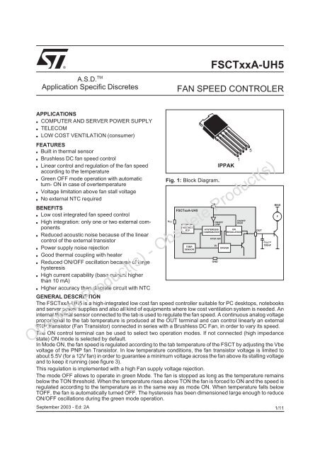
FSCTxxA-UH5<br />
<strong>FAN</strong> <strong>SPEED</strong> <strong>CONTROLER</strong><br />
Fig. 1: Block Diagram.<br />
VCC<br />
FSCTxxA-UH5<br />
VOLTAGE<br />
REF.<br />
GND<br />
IPPAK<br />
ON/OFF<br />
LOW<br />
HYSTERESIS<br />
COMPARATOR<br />
HYST.-EN<br />
VT<br />
DRIVER<br />
1<br />
ON/OFF<br />
HIGH<br />
ON<br />
REGULATION<br />
GENERAL DESCRIPTION<br />
The FSCTxxA-UH5 is a high-integrated low cost fan speed controller suitable for PC desktops, notebooks<br />
and server power supplies and also all kind of equipments where low cost ventilation system is needed. An<br />
internal thermal sensor connected to the tab is used to regulate the fan speed. A continuous analog voltage<br />
proportional to the tab temperature is produced at the OUT terminal and can control linearly an external<br />
PNP transistor (Fan Transistor) connected in series with a Brushless DC Fan, in order to vary its speed.<br />
The ON control terminal can be used to select two operation modes. If not connected (high impedance<br />
Obsolete Product(s) - Obsolete Product(s)<br />
state) ON mode is selected by default.<br />
In Mode ON, the fan speed is regulated according to the tab temperature of the FSCT by adjusting the Vbe<br />
voltage of the PNP fan Transistor. In low temperature conditions, the fan transistor voltage is limited to<br />
about 5.5V (for a 12V fan) in order to guarantee a minimum voltage across the fan above its stalling voltage<br />
and to keep it running (see figure 3).<br />
This regulation is implemented with a high Fan supply voltage rejection.<br />
The mode OFF allows to operate in green Mode. The fan is stopped as long as the temperature remains<br />
below the TON threshold. When the temperature rises above TON the fan is forced to ON and the speed is<br />
regulated according to the temperature as in the same way as mode ON. When temperature falls below<br />
TOFF, the fan is automatically turned OFF. The hysteresis has been dimensioned large enough to reduce<br />
ON/OFF oscillations during the green mode operation.<br />
TEMP.<br />
SENSOR<br />
ON<br />
5<br />
OUT<br />
C OUT=<br />
100nF<br />
BIAS<br />
F<br />
1/11
FSCTxxA-UH5<br />
PINT OUT DESIGNATION<br />
Pint Out<br />
designation<br />
Description Pin<br />
TEST Test pin (must not be connected) 1<br />
VCC Operating DC supply 2<br />
GND Ground (internally connected to the tab) 3<br />
ON Mode ON and OFF selection 4<br />
OUT Output (connect to PNP fan transistor base) 5<br />
ABSOLUTE MAXIMUM RATINGS<br />
Symbol Parameter Value Unit<br />
VCC Supply voltage referenced to GND -0.3 to 20 V<br />
Tj Operating junction temperature 0 to 125 °C<br />
Tstg Storage temperature -65 to 150 °C<br />
TL Lead temperature (double wave soldering) 260 °C<br />
Maximum voltage at any pin VCC V<br />
Minimum voltage at any pin -0.3 V<br />
ESD Electrostatic discharge immunity at each terminal<br />
(human body model)<br />
2 kV<br />
ELECTRICAL CHARACTERISTICS (Continue)<br />
VCC from 9Vdc to 15Vdc, Cout = 100nF, Tj = 0°C to 125°C, otherwise specified<br />
Symbol<br />
SUPPLY<br />
Parameter Test conditions<br />
Min.<br />
Value<br />
Typ. Max.<br />
Unit<br />
ICCmax<br />
DRIVER<br />
Operating supply current VON =5Vor0V<br />
VCC = 12V<br />
1.1 3 mA<br />
IOL Sinking current capability<br />
at the OUT terminal<br />
VOUT =VOL and Tj = 125°C 10 mA<br />
ILEAK Maximum sink leakage<br />
current at OUT pin (mode<br />
OFF)<br />
VOUT = 20V, VON =0V<br />
Tj= 50°C<br />
10 µA<br />
Obsolete Product(s) - Obsolete Product(s)<br />
2/11<br />
VOL<br />
VOMS<br />
Minimum voltage at the<br />
OUT terminal (mode ON)<br />
OUT voltage for minimum<br />
fan speed (mode<br />
ON)<br />
VON = 5V, Tj = 125°C 0.55 0.7 V<br />
VON = 5V, Tj from 0°C to TMS 5.3 5.5 V<br />
Static line regulation VCC = 9V to 15V, VON =5V<br />
Tj= 25°C<br />
0.5 mV/V<br />
KSL VOUT temperature slope VOUT = 80%<br />
VOMS to<br />
20% VOMS<br />
FSCT17A-UH5<br />
FSCT11A-UH5<br />
FSCT07A-UH5<br />
155<br />
100<br />
68<br />
165<br />
107<br />
72<br />
175<br />
114<br />
77<br />
mV/°C
ELECTRICAL CHARACTERISTICS (Continue)<br />
VCC within the supply voltage range, Cout = 100nF, Tj = 0°C to 125°C, otherwise specified<br />
FSCTxxA-UH5<br />
Symbol Parameter Test conditions<br />
Min.<br />
Value<br />
Typ. Max.<br />
Unit<br />
TEMPERATURE MANAGEMENT (all T° threshold are guaranteed by design)<br />
TMS Temperature regulation<br />
threshold<br />
VOUT =VOMS<br />
VON =5V<br />
32 37 42 °C<br />
TON OFF mode switch ON<br />
temperature<br />
VCC = 12V<br />
VON =0V<br />
66 71 76 °C<br />
TOFF OFF mode switch OFF<br />
temperature<br />
VCC = 12V<br />
VON =0V<br />
34 39 44 °C<br />
TOL Minimum temperature<br />
for maximum speed<br />
VCC = 12V<br />
VON =5V<br />
VOUT =VOL<br />
FSCT17A-UH5<br />
FSCT11A-UH5<br />
FSCT07A-UH5<br />
61<br />
76<br />
97<br />
66<br />
81<br />
102<br />
71<br />
86<br />
107<br />
°C<br />
TV3 Tab temperature for<br />
VOUT =3V (*)<br />
(see figure 3)<br />
VOUT =3V<br />
VON =5V<br />
FSCT17A-UH5<br />
FSCT11A-UH5<br />
49<br />
56<br />
52<br />
59<br />
55<br />
62<br />
°C<br />
FSCT07A-UH5 66 69 72<br />
ON SIGNAL<br />
VIH Voltage range for ON mode 1 V<br />
VIL Voltage range for OFF mode 0.3 V<br />
IS Source current at the<br />
ON pin (see figure 2)<br />
VCC = 12V<br />
ON terminal shorted to ground<br />
10 25 µA<br />
(*) Absolute temperature dissipation applicable on all VOUT range between VOMS and VOL<br />
THERMAL PARAMETERS<br />
Symbol Parameter Value Unit<br />
Rth(j-c) Thermal resistance junction to case 3 °C/W<br />
Fig. 2: "ON" input schematic diagram.<br />
Obsolete Product(s) - Obsolete Product(s)<br />
ON<br />
IS<br />
50k<br />
VCC<br />
To other blocks<br />
3/11
FSCTxxA-UH5<br />
Fig. 3: Temperature slopes.<br />
Fig. 4: ICC versus VCC for mode ON.<br />
I CC(mA)<br />
1.5<br />
1.4<br />
1.3<br />
1.2<br />
1.1<br />
1<br />
0.9<br />
0.8<br />
0.7<br />
0.6<br />
0.5<br />
Obsolete Product(s) - Obsolete Product(s)<br />
4/11<br />
V = 5.3V<br />
OMS<br />
Tj = 25°C<br />
V = 3V<br />
OUT<br />
V = 0.6V<br />
OL<br />
V (V )<br />
OUT DC<br />
9 11 13 15 17 19<br />
V CC(V)<br />
FSCT17A-UH5<br />
165mV/°C<br />
Tj = 125°C<br />
FSCT11A-UH5<br />
107mV/°C<br />
T MS=37 TV3 T OL=66<br />
TV3<br />
TV3<br />
FSCT07A-UH5<br />
72mV/°C<br />
T OL=81 T OL=102<br />
Fig. 5: ICC versus VCC test circuit (mode ON).<br />
VON 1V<br />
VCC<br />
A<br />
VCC<br />
ON<br />
T (°C)<br />
j<br />
ICC<br />
OUT<br />
GND<br />
V<strong>FAN</strong> 12V<br />
3.8k<br />
100nF
DETAILED DESCRIPTION & APPLICATION INFORMATION<br />
1. OUTPUT CHARACTERISTIC VERSUS TEMPERATURE<br />
FSCTxxA-UH5<br />
1.1 <strong>FAN</strong> speed control<br />
As it's well known, BRUSHLESS DC motors present the advantage of a quasi-linear speed-voltage characteristic.<br />
Hence, the fan speed is varying linearly versus the voltage which is applied across its terminals.<br />
The FSCT Integrated Circuit provides at its OUT terminal, a voltage which changes versus the temperature<br />
sensed through its tab. This OUT voltage decreases as temperature increases, following two modes of operation.<br />
By connecting this OUT terminal to the Base of a PNP transistor, as shown in figure 1, the <strong>FAN</strong><br />
voltage will increase with the sensed temperature.<br />
The <strong>FAN</strong> voltage is given by the following equation:V<strong>FAN</strong> = V<strong>FAN</strong> + −VEB −VOUT<br />
(1)<br />
Typically, for a 12 V V<strong>FAN</strong>+ anda1VVEB voltage, this gives:V = 11 −V<br />
(2)<br />
<strong>FAN</strong> ( V ) OUT ( V )<br />
It can be noticed that the PNP operates as a linear amplifier. This avoids EMI and acoustic noise compared<br />
to Pulse Width Modulation control circuits.<br />
1.2 ON/OFF Mode Selection<br />
The figure 6 gives the algorithm flowchart of the FSCT behavior. First, two modes of operation are distinguished<br />
by the ON pin signal.<br />
■ Mode ON: activated when ON pin is at High Level or Not Connected (thanks to an internal Pull-up<br />
curren source "IS")<br />
■ Mode OFF: activated when ON pin is at Low Level.<br />
During Mode ON, the OUT voltage follows a three-parts characteristic, according to its junction temperature<br />
(Tj):<br />
■ Tj T OL<br />
yes<br />
<strong>FAN</strong> OFF<br />
V OUT =V CC<br />
no<br />
T j
FSCTxxA-UH5<br />
2. Hysteresis control (mode OFF)<br />
FSCT can be shut down by the ON signal. When, this signal is low, the OUT pin is at high level, i.e. the <strong>FAN</strong><br />
is turned off.<br />
This mode enables to save the energy wasted by the <strong>FAN</strong> in case of operations at very low output power.<br />
For a 12 V supply voltage, the shut-down of the <strong>FAN</strong> brings a 0.5 to 2.5 W power saving (for a 200 mA 12 V<br />
DC motor).<br />
During the mode OFF, the FSCT doesn't lose temperature control; indeed, in case of over-temperature,<br />
the <strong>FAN</strong> is automatically switched on. This safety feature protects the power supply or the semiconductor<br />
devices from unexpected over-temperature.<br />
In order to keep the energy saving benefit, the FSCT turns back off the <strong>FAN</strong> when the temperature falls below<br />
TOFF threshold.<br />
In practice, three cases can appear for a constant applied heating power (for instance, the output power of<br />
the power supply where the FSCT is used) (cf. figure 8):<br />
■ Case 1: the heating power is too low, and keeps Tj below TON. The <strong>FAN</strong> remains OFF.<br />
■ Case 2: the heating power is high enough to raise Tj above TON. But, as this power is quite low, Tj falls<br />
down TOFF, and the temperature starts again to increase, up to TON. This results in a <strong>FAN</strong> ON/OFF periodical<br />
cycle.<br />
■ Case 3: the heating power is higher that in case 2, so that Tj remains above TOFF. The <strong>FAN</strong> stays ON<br />
in that case, unless the heating power decreases.<br />
For example, with a 200 W computer power supply, working with a FSCT17 device put on the power semiconductors<br />
heatsink, Case 1 could be reached for a 25 W output power consumption (Tj will stabilize<br />
around 60 °C, i.e. below typical TON).<br />
Case 2 could be reached for a 50 W power consumption. Then, thanks to the large Hysteresis value (30 °C<br />
typ.), the ON/OFF period (refer to TP on figure 8) lasts approximately 15 minutes. This is long enough to<br />
avoid too many <strong>FAN</strong> starts-up cycle per hour.<br />
Case 3 could be reached for a 75W, or higher, power consumption. For 75W, the power supply ambient<br />
temperature stabilizes itself around 42°C.<br />
It should be noted that, for Case 3, such steady state points of operation, are allowed due to the fact that the<br />
OUT voltage follows the same linear law as that in ON mode. Then, the Hysteresis control is smarter than a<br />
simple ON/OFF control mode.<br />
Fig. 7: OUT voltage versus junction temperature.<br />
Obsolete Product(s) - Obsolete Product(s)<br />
6/11<br />
VOUT<br />
VCC<br />
VOMS<br />
1V<br />
VOL<br />
Mode ON<br />
TMS<br />
TOFF<br />
TOL TON<br />
Mode OFF<br />
T (°C)<br />
j
Fig. 8: Temperature evolution cases in mode OFF.<br />
Tj<br />
TON<br />
TOFF<br />
3. Internal temperature sensor<br />
3<br />
FSCTxxA-UH5<br />
Time<br />
3.1 Temperature sensor linear response<br />
FSCT devices feature an internal temperature sensor. This sensor results directly from silicon properties. It<br />
is actually a voltage reference which is proportional to the absolute temperature, as it is an image of the Silicon<br />
thermal voltage "Vt" (refer to the following equation).<br />
k : Boltzmann cons tant<br />
k ⋅T Vt = with: T: absolute temperature ( K )<br />
q<br />
q = 16 . ⋅10<br />
19 −<br />
⎧<br />
⎪<br />
⎨<br />
⎪<br />
⎩<br />
C<br />
This sensing method, which presents a positive temperature coefficient of +2mV/°C is preferred to a VBE<br />
sensing method (-2mV/°C, sometimes used in thermal protections) because of its better accuracy (low impact<br />
of process dispersions).<br />
This signal is then processed to provide the desired OUT voltage range.<br />
This internal sensor allows users not to use a Negative Temperature Coefficient thermistor (NTC).<br />
Hence, users get rid of Joule effect, due to NTC bias current, that disturbs the temperature measurement.<br />
Furthermore, the FSCT response is linear with the temperature. This simplifies the thermal study and the<br />
heat sink rating for the power supply components or for the microprocessor.<br />
NTC thermistors users need also to add a fixed resistor in order to get a linear thermal response from such<br />
kind of sensor. The linear behavior is also only ensured for a restricted temperature range.<br />
Obsolete Product(s) - Obsolete Product(s)<br />
3.2 IPPAK mounting considerations<br />
First, it should be noted that the tab is directly connected to the GND pin; then care must be taken when the<br />
FSCT is glued to a heatsink. If this heatsink is at a differential voltage that the Ground, an electrical insulator<br />
has to be added between the tab and the heat-sink.<br />
Using non-isolated Through-Hole package like the IPPAK offers also a lot of benefits, compared to NTC<br />
bulbs. Indeed, NTC do not offer a flat area like IPPAK package. Users need to add some glue to ensure<br />
contact of the NTC bulb and the heat sink, at the cost of an increase in the thermal impedance and<br />
response.<br />
TP<br />
2<br />
1<br />
7/6
FSCTxxA-UH5<br />
Two components should be used to improve the heat exchange between the FSCT die and the heat sink,<br />
that the temperature has to be monitored. These components are:<br />
■ A thermal interface pad, in order to reduce the impact of air voids on the thermal impedance and to ensure<br />
an electrical insulation (if needed)<br />
■ A clip to push the IPPAK against the heat sink and then to reduce also the interface thermal impedance.<br />
Several clips can be used depending on the heat sink type:<br />
■ Saddle clips (cf. figure 9) for slim heat sink;<br />
■ U-clips (cf. figure 10) for thick heat sink<br />
■ Dedicated clips for special shape heat sink.<br />
Fig. 9: IPPAK mounted with a Saddle clip. Fig. 10: IPPAK mounted with a U-clip.<br />
It can be noticed that the thickness of the IPPAK package (2.3 +/- 0.1 mm) is similar to those of SOT-32 and<br />
SOT-82 (2.55 +/- 0.15 mm). The same clips can so be used for all these packages.<br />
3.3 Temperature measurement error<br />
Firstly, the time constant between a temperature variation on the external side on the IPPAK copper tab,<br />
and the silicon die is in the range of a few hundred of milliseconds. As temperature phenomena are extremely<br />
slow for the targeted applications (the temperature of a MOSFET heat sink, increases typically with<br />
an 1°C per second rate, in a power supply), the FSCT is able to react immediately to over-heating events.<br />
Moreover, the very low junction to case thermal resistance (3 °C/W) reduces as much as possible the temperature<br />
measurement error.<br />
We calculate, in the following, this error considering both the package and the heatsink-Tab interface thermal<br />
resistances (figure 11).<br />
Several companies offer adhesive and isolating<br />
materials to be used as interface between electronic<br />
devices and a heat sink. These interfaces<br />
can be provided with a shape dedicated for the<br />
Tab foot print. For the IPPAK package, users could<br />
choose a shape dedicated for SOT-32, SOT-82 or<br />
even TO-126 or TO-220 packages (the more can<br />
do the less).<br />
Obsolete Product(s) - Obsolete Product(s)<br />
8/11<br />
Fig. 11: IPPAK Heatsink Interface.<br />
Interface
FSCTxxA-UH5<br />
These interfaces offer very low thermal resistance. For example, the Sil-Pad ® 800 family, from<br />
BERGQUIST, which is designed for low cost applications and low mounting pressures, present a typical<br />
thermal impedance of 0.45 °C.in²/W. This impedance can increase up to 0.92 °C.in²/W for a 10 psi pressure,<br />
which is below the normal atmospheric one (1 atm = 1013 hPa = 1013 x 100 x 14.5 x 10-3 = 14.7 psi).<br />
Furthermore, a mounting clip will apply a force between 15 to 50 N. This leads to a 25 to 200 psi pressure.<br />
In this case, the thermal impedance varies from 0.6 to 0.29 °C.in²/W for the Sil-Pad ® 800 family.<br />
For the example, we take the worst case hypothesis of a 1°C.in²/W interface between the FSCT case and<br />
the heat sink.<br />
We take into account only the tab surface for the heat exchange. This surface equals typically:<br />
S = 4.7 x 5.1 mm2 = 0.037 in2 This yields to a supplementary resistance of: Rthc-h = 1/0.037 = 27°C/W<br />
Then, the maximum power dissipated in the FSCT, for the maximum output power, is given by the following<br />
equation:<br />
Pmax = ICC ⋅ VCC + IOUT ⋅VOMS<br />
The following numerical application gives (for a 150 mA <strong>FAN</strong> DC current, a 80 gain for the PNP and a 12 V<br />
power supply):<br />
IOUT = 150 / 80 = 1.87mA<br />
−3 −3<br />
Pmax = 3 × 12 × 10 + 187 . × 5. 5 × 10 = 46mW<br />
Then, the temperature error is: ΔT = 0. 046 × ( 3 + 27) = 138 . ° C<br />
The temperature sensing error can then be neglected whan one considers the operation range (from 0 to<br />
100 °C), even with low cost interface material and without any mounting clip. For example, with a higher<br />
pressure, thanks to a clip, this error could be divided by three.<br />
4. TEMPERATURE/VOLTAGE SLOPE CHANGE<br />
The OUT voltage versus temperature characteristic of the FSCT has been designed to fit majority cases of<br />
application, in the field of PC power supplies.<br />
The advantage for the user is to have a minimum count of components while achieving a smart<br />
temperature regulation.<br />
Nevertheless, some applications require dedicated temperature regulation characteristic. Figure 13<br />
provides an example of a solution which allows to change the ratio between PNP base voltage and the<br />
temperature. This schematic only requires a dual<br />
single-voltage amplifier (in DIL8 package for Fig. 12: Modified characteristics.<br />
example) and less than ten supplementary<br />
resistors.<br />
This schematic keeps the advantage of applying a<br />
VOUT<br />
constant minimum voltage (VOMS) below TMS temperature.<br />
Indeed, the U1A operational amplifier<br />
subtracts 5.1 V (thanks to the D1 Zener diode, refer<br />
to VREF) from VOUT. This means that the ratio<br />
VNEW<br />
change is only taken into account when VOUT is<br />
Mode OFF<br />
lower than 5.1 V. For higher voltages (VOMS in mode<br />
ON or VCC in mode OFF), the new base to GND volt-<br />
VOMS<br />
Mode ON<br />
Obsolete Product(s) - Obsolete Product(s)<br />
age (VNEW) remains the same (cf. figure 12).<br />
So, if one wants to increase accurately the<br />
Step-down<br />
voltage-temperature ratio, i.e. that VOUT will<br />
decrease more quickly when Tj increases, figure<br />
13 schematics should be implemented. Indeed,<br />
the voltage at the operational amplifier U1B (which<br />
acts as a follower) output is:<br />
⎧VNEW<br />
= VOUT if VOUT > VREF<br />
⎪<br />
⎨<br />
RN<br />
VNEW = VOUT<br />
− ⋅( VREF −VOUT ) otherwise<br />
⎩<br />
⎪<br />
RD<br />
TOFF<br />
TON<br />
T (°C)<br />
j<br />
9/11
FSCTxxA-UH5<br />
Fig. 13: Step-down OUT voltage schematic.<br />
VCC<br />
Obsolete Product(s) - Obsolete Product(s)<br />
10/11<br />
R3<br />
1k<br />
U2<br />
2 5<br />
VCC OUT<br />
4<br />
1<br />
3<br />
VCC<br />
ON<br />
TEST<br />
GND<br />
FSCT<br />
DZ<br />
5V1<br />
R4<br />
{RD}<br />
V REF<br />
R1<br />
{RD}<br />
C1<br />
2n2<br />
2<br />
3<br />
R5<br />
{RN}<br />
-<br />
+<br />
R2<br />
8 4<br />
{RN}<br />
V<br />
R7<br />
{RF}<br />
OUT<br />
U1A<br />
MC33172<br />
1<br />
VCC<br />
R6<br />
{RF}<br />
R8<br />
{RF}<br />
PARAMETERS:<br />
RD = 33k<br />
RN = 68k<br />
RF = 130k<br />
6<br />
5<br />
-<br />
+<br />
R9<br />
{RF}<br />
U1B<br />
MC33172<br />
7<br />
V<br />
1<br />
2<br />
NEW<br />
VCC<br />
M1<br />
<strong>FAN</strong> MOTOR<br />
Q1<br />
2N2907
PACKAGE MECHANICAL DATA<br />
IPPAK<br />
H<br />
L<br />
L1<br />
e<br />
E<br />
B2<br />
G1<br />
G<br />
B3<br />
B<br />
B6<br />
V1<br />
B5<br />
L2<br />
A1<br />
FSCTxxA-UH5<br />
Order code Marking Package Weight Delivery mode Base qty<br />
FSCT17A-UH5 FSCT17A<br />
FSCT11A-UH5 FSCT11A<br />
FSCT07A-UH5 FSCT07A<br />
C2<br />
A<br />
C<br />
D<br />
REF.<br />
DIMENSIONS<br />
Millimeters Inches<br />
Min. Typ. Max Min. Typ. Max.<br />
A 2.20 2.40 0.086 0.094<br />
A1 0.90 1.10 0.035 0.043<br />
B 0.40 0.60 0.015 0.023<br />
B2 5.20 5.40 0.204 0.212<br />
B3 0.70 0.027<br />
B5 0.30 0.011<br />
B6 1.00 0.039<br />
C 0.45 0.60 0.017 0.023<br />
C2 0.48 0.60 0.018 0.023<br />
D 6.00 6.20 0.236 0.244<br />
E 6.40 6.60 0.215 0.259<br />
e 1.27 0.050<br />
G 4.9 5.25 0.192 0.206<br />
G1 2.38 2.70 0.093 0.106<br />
H 15.90 16.30 0.625 0.641<br />
L 9.00 9.40 0.354 0.370<br />
L1 0.80 1.20 0.031 0.047<br />
L2 0.80 1.00 0.031 0.039<br />
V1 10° 10°<br />
IPPAK 0.4 g Tube 75<br />
Information furnished is believed to be accurate and reliable. However, <strong>STMicroelectronics</strong> assumes no responsibility for the consequences of<br />
use of such information nor for any infringement of patents or other rights of third parties which may result from its use. No license is granted by<br />
implication or otherwise under any patent or patent rights of <strong>STMicroelectronics</strong>. Specifications mentioned in this publication are subject to<br />
change without notice. This publication supersedes and replaces all information previously supplied. <strong>STMicroelectronics</strong> products are not authorized<br />
for use as critical components in life support devices or systems without express written approval of <strong>STMicroelectronics</strong>.<br />
The ST logo is a registered trademark of <strong>STMicroelectronics</strong>.<br />
All other names are the property of their respective owners.<br />
© 2003 <strong>STMicroelectronics</strong> - All rights reserved.<br />
<strong>STMicroelectronics</strong> GROUP OF COMPANIES<br />
Australia - Belgium - Brazil - Canada - China - Czech Republic - Finland - France - Germany -<br />
Hong Kong - India - Israel - Italy - Japan - Malaysia - Malta - Morocco - Singapore - Spain -<br />
Sweden - Switzerland - United Kingdom - United States<br />
www.st.com<br />
Obsolete Product(s) - Obsolete Product(s)<br />
11/11