Elektronenstrahlhärtung von Lacken_EN_V2_1_net

You also want an ePaper? Increase the reach of your titles
YUMPU automatically turns print PDFs into web optimized ePapers that Google loves.
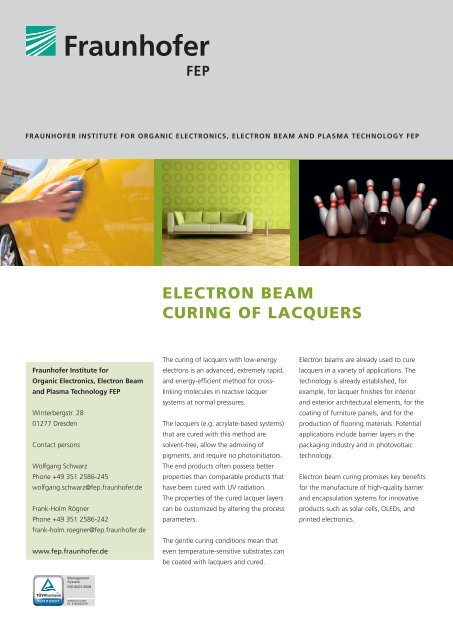
FRAUNHOFER INSTITUTE FOR ORGANIC ELECTRONICS, ELECTRON BEAM AND PLASMA TECHNOLOGY FEP<br />
ELECTRON BEAM<br />
CURING OF LACQUERS<br />
Fraunhofer Institute for<br />
Organic Electronics, Electron Beam<br />
and Plasma Technology FEP<br />
Winterbergstr. 28<br />
01277 Dresden<br />
Contact persons<br />
Wolfgang Schwarz<br />
Phone +49 351 2586-245<br />
Frank-Holm Rögner<br />
Phone +49 351 2586-242<br />
The curing of lacquers with low-energy<br />
electrons is an advanced, extremely rapid,<br />
and energy-efficient method for crosslinking<br />
molecules in reactive lacquer<br />
systems at normal pressures.<br />
The lacquers (e.g. acrylate-based systems)<br />
that are cured with this method are<br />
solvent-free, allow the admixing of<br />
pigments, and require no photoinitiators.<br />
The end products often possess better<br />
properties than comparable products that<br />
have been cured with UV radiation.<br />
The properties of the cured lacquer layers<br />
can be customized by altering the process<br />
parameters.<br />
Electron beams are already used to cure<br />
lacquers in a variety of applications. The<br />
technology is already established, for<br />
example, for lacquer finishes for interior<br />
and exterior architectural elements, for the<br />
coating of furniture panels, and for the<br />
production of flooring materials. Potential<br />
applications include barrier layers in the<br />
packaging industry and in photovoltaic<br />
technology.<br />
Electron beam curing promises key benefits<br />
for the manufacture of high-quality barrier<br />
and encapsulation systems for innovative<br />
products such as solar cells, OLEDs, and<br />
printed electronics.<br />
www.fep.fraunhofer.de<br />
The gentle curing conditions mean that<br />
even temperature-sensitive substrates can<br />
be coated with lacquers and cured.
Properties of the cured lacquers<br />
Applications<br />
Our offer<br />
▪▪very low emissions<br />
▪▪high resistance to chemicals<br />
▪▪UV resistance; yellowing does not occur<br />
as no photoinitiators are used<br />
▪▪resistant to elevated temperatures<br />
▪▪high abrasion resistance<br />
▪▪good adhesion on plastic substrates<br />
▪▪uniform lacquer quality<br />
Advantages of the technology<br />
▪▪environmentally friendly, as no solvents<br />
or photoinitiators are used<br />
▪▪energy-efficient<br />
▪▪very fast processing (up to 600 m/min)<br />
and very rapid curing<br />
▪▪can be used with a large variety of<br />
reactive lacquer systems (liquid, powder,<br />
water-soluble, pure substances or<br />
mixtures, biodegradable, biocompatible)<br />
and on a variety of substrates (rigid<br />
or flexible, also temperature-sensitive<br />
substrates)<br />
▪▪the properties of the lacquers<br />
(e.g. surface topography, printing<br />
properties, hardness/elasticity, gloss/<br />
brilliance, depth of hardening) can be<br />
very accurately set by altering the process<br />
parameters such as the dose of energy<br />
▪▪easy processing with low-energy<br />
electrons at normal pressure<br />
▪▪in-line monitoring of the electron beam<br />
power and immediate in-line layer<br />
analysis possible<br />
▪▪curing as a finishing process possible<br />
The technology can be applied to a wide<br />
range of materials. Surface layers down to<br />
a depth of 0.2 mm can be cured.<br />
▪▪flat and 3-D substrates, bulk goods<br />
▪▪car and machine parts<br />
▪▪furniture/doors, flooring (polymers/wood)<br />
▪▪coil coating (sheet materials/white goods)<br />
▪▪special papers, wall coverings, films<br />
(for barriers, packaging, printing, gloss<br />
effects, release films)<br />
▪▪glass articles, architectural glass,<br />
abrasion-resistant layers for optics<br />
▪▪exterior facade elements and interior<br />
architectural elements made of inorganic,<br />
ceramic, metallic, or polymeric materials<br />
▪▪barrier and encapsulation layers for<br />
photovoltaic technology and printed<br />
electronics<br />
We offer:<br />
▪▪expert advice about the technology and<br />
customization to your needs<br />
▪▪selection, testing, and appraisal of<br />
popular commercial electron beam<br />
generators<br />
▪▪development of customer-specific<br />
electron beam generators<br />
▪▪feasibility studies<br />
▪▪pilot trials<br />
▪▪servicing of electron beam generators<br />
▪▪optimization of existing process<br />
technologies (energy, electron beam<br />
power, beam guidance, product<br />
transport)<br />
▪▪accompanying tests for selecting suitable<br />
lacquer systems and for development of<br />
lacquer formulations<br />
▪▪accompanying process and product<br />
analysis<br />
Schematic representation of lacquer curing with an electron beam<br />
beam exit window<br />
uncured lacquer<br />
product transport<br />
electron beam generator<br />
divergent electron beam<br />
cured lacquer<br />
© FRAUNHOFER FEP – 2.1 – D11