about your cleaning process we care... - BluOcean.AdMedia
about your cleaning process we care... - BluOcean.AdMedia
about your cleaning process we care... - BluOcean.AdMedia

Create successful ePaper yourself
Turn your PDF publications into a flip-book with our unique Google optimized e-Paper software.
www.globalsmtseasia.com<br />
www.globalsmtindia.in<br />
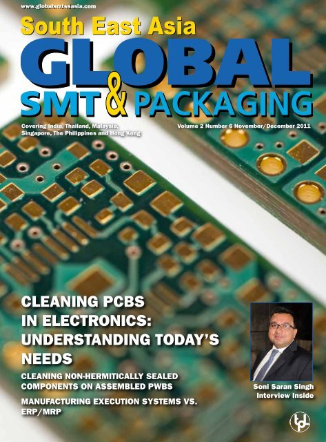
South East Asia<br />
Covering India, Thailand, Malaysia,<br />
Singapore, The Philippines and Hong Kong<br />
CleaNINg PCBS<br />
IN eleCTroNICS:<br />
uNDerSTaNDINg ToDay’S<br />
NeeDS<br />
CleaNINg NoN-HerMITICally SealeD<br />
CoMPoNeNTS oN aSSeMBleD PWBS<br />
MaNufaCTurINg exeCuTIoN SySTeMS VS.<br />
erP/MrP<br />
Volume 2 Number 6 November/December 2011<br />
Soni Saran Singh<br />
Interview Inside
South East Asia<br />
Global SMT & Packaging<br />
is distributed by controlled<br />
circulation to qualified<br />
personnel. For all others,<br />
subscriptions are available at<br />
a cost of $19.99 for the<br />
current volume (six issues).<br />
No part of this publication may<br />
be reproduced, stored in a<br />
retrieval system, transmitted<br />
in any form or by any means<br />
electronic, mechanical,<br />
photocopying, recording<br />
or otherwise without prior<br />
written consent of the<br />
publisher. No responsibility is<br />
accepted for the accuracy of<br />
information<br />
contained in the text,<br />
illustrations or<br />
advertisements. The opinions<br />
expressed in the articles are<br />
not necessarily those of the<br />
editors or publisher.<br />
© Trafalgar Publications Ltd<br />
Designed and Published by<br />
Trafalgar Publications Ltd,<br />
Bournemouth, UK<br />
DOwnLOAD ThIS<br />
ISSuE TO yOuR<br />
MObILE PhOnE:<br />
If you don’t already have one, search<br />
for a QR code reader app in <strong>your</strong><br />
smartphone’s app marketplace.<br />
Then use it to scan the code above<br />
& download this magazine issue<br />
right to <strong>your</strong> phone.<br />
www.globalsmtseasia.com<br />
Contents<br />
EDITORIAL<br />
2 Editorial<br />
Usha Prasad<br />
TEChnOLOGy FOCuS<br />
8 Cleaning PCBs in electronics: understanding<br />
today’s needs<br />
P.J.Duchi, Anne-Marie Laügt, Marie Verdier,<br />
G.Abidh, Inventec Performance Chemicals<br />
12 Manufacturing execution systems vs. ERP/MRP<br />
Bill Crowley, Optimal Electronics<br />
20 Reducing graping through <strong>process</strong> optimization<br />
Ed Briggs and Ron Lasky, Indium Corporation<br />
28 Area ratios of 0.40 and 0.48 with nano-coated<br />
stencils<br />
Carmina Läntzsch, LaserJob<br />
30 Cleaning non-hermitically sealed components on<br />
assembled PWBs<br />
Mike Bixenman, D.B.A., Kyzen Corporation<br />
SPECIAL FEATuRES<br />
18 Case Study: Full-service EMS provider adds AXI<br />
for full coverage<br />
32 Interview—Soni Saran Singh, NMTronics<br />
34 India plays host to SMaLED 2011, the first-ever<br />
conference on surface mount & LED<br />
REGuLAR COLuMnS<br />
24 Slow global growth at year end<br />
Walt Custer and Jon Custer-Topai<br />
OThER REGuLAR FEATuRES<br />
4 Industry News<br />
35 New Products<br />
36 International Diary<br />
Contents<br />
Volume 2, No. 6<br />
November/December 2011<br />
Visit www.globalsmtseasia.com for the latest news and more, every day.<br />
8<br />
12<br />
20<br />
Global SMT & Packaging South East Asia – May/June 2011 – 1
Title Editorial<br />
www.globalsmtseasia.com<br />
news@globalsmt.net<br />
editorial offices<br />
Europe<br />
Trafalgar Publications<br />
Global SMT & Packaging<br />
Crown House, 72 Hammersmith Rd,<br />
Hammersmith, London, W14 8TH<br />
United Kingdom<br />
Tel: +44 7924 581 523<br />
United States<br />
Global SMT & Packaging<br />
PO Box 7579<br />
Naples, FL 34102, USA<br />
Tel: +1 (239) 245-9264<br />
Fax: (239) 236-4682<br />
China<br />
Global SMT & Packaging<br />
Electronics Second<br />
Research Institute<br />
No.159, Hepin South Road<br />
Taiyuan City, PO Box 115, Shanxi,<br />
Province 030024, China<br />
Tel: +86 (351) 652 3813<br />
Fax: +86 (351) 652 0409<br />
Editor-in-Chief<br />
Trevor Galbraith<br />
Tel: +44 7924 581 523 (Europe)<br />
Tel: +44 20 7792 0792 (UK)<br />
Tel: +1 (239) 245-9264 x101 (US)<br />
editor@globalsmt.net<br />
Managing Editor<br />
Heather Lackey<br />
Tel: +1 (239) 245-9264 x105<br />
hglackey@globalsmt.net<br />
Technical Editor<br />
Usha Prasad<br />
uprasad@trafalgarmedia.com<br />
Circulation & Subscriptions<br />
Kelly Grimm<br />
Tel: +1 (239) 245-9264 x106<br />
subscriptions@globalsmt.net<br />
advertising<br />
India—Amitava Sarkar<br />
09379229397<br />
asarkar@trafalgarmedia.com<br />
Singapore & Hong Kong—<br />
Philip Lim<br />
+65 6552-7388<br />
bluocean.admedia@gmail.com<br />
Korea—Amy Kim<br />
akim@globalsmt.net<br />
Americas—Shana Harris<br />
Tel:+1 (239) 245-9264 x101<br />
sharris@trafalgarmedia.com<br />
Europe—Alex Klocksin<br />
Tel: +49.1577.893.4884<br />
aklocksin@globalsmt.net<br />
Usha Prasad<br />
Technical Editor<br />
editorial<br />
Greetings friends!<br />
This is my maiden editorial. In the<br />
beginning, I would like to talk a bit<br />
<strong>about</strong> the future of mobile devices. Mobile<br />
will soon go on to become the primary digital<br />
connection to <strong>your</strong> customers. It must<br />
be noted that consumer spending is also<br />
increasing, and with it advertising spend<br />
and investment in mobile services.<br />
It is now being said that the future of<br />
mobile is context. Indeed, that seems to be<br />
so!<br />
According to Julie A. Ask, vice president,<br />
principal analyst, Forrester, context<br />
will include the following:<br />
• Situation: the current location,<br />
altitude, and speed the customer is<br />
experiencing;<br />
• Preferences: the history and personal<br />
decisions the customer has<br />
shared with you; and<br />
• Attitudes: the feelings or emotions<br />
implied by the customer’s actions<br />
and logistics.<br />
As of today, context seems to be mostly<br />
<strong>about</strong> location. Ho<strong>we</strong>ver, all of that is<br />
<strong>about</strong> to get a lot more interesting over the<br />
coming months.<br />
Future cell phones can be expected to<br />
have some or all of the following technologies,<br />
if not more: 3D cameras, near-field<br />
communications (NFC), biometrics, gesture<br />
control, 3D displays, micro-mirrors,<br />
augmented reality, pico-projectors, gesture<br />
control, and so on! There are many, many<br />
other technologies, not mentioned here,<br />
that will likely make their way into the<br />
mobile phones of tomorrow. The forthcoming<br />
sensors will add new contextual<br />
elements as <strong>we</strong>ll. Also, it is expected that<br />
augmented reality will move into stores,<br />
airports, etc.<br />
Does <strong>your</strong> cell phone even resemble<br />
all of this today? Some of you have Apple<br />
iPhones and some others have smartphones<br />
from other leading vendors. You<br />
must be wondering: where am I getting all<br />
this information from? Or even, how will<br />
the mobile phone support all of these applications?<br />
Do not worry! The handset vendors are<br />
working overtime in an effort to add these,<br />
and many other futuristic applications on to<br />
<strong>your</strong> cell phone. In many companies, software<br />
is driving the new wave of innovation<br />
for smarter products and services. Even as<br />
<strong>we</strong> speak, they are managing requirements<br />
across various lifecycle and disciplines.<br />
These global companies are attempting<br />
to build the right kind of product with<br />
structural and behavioural analysis and<br />
design. For them, it is very critical that they<br />
understand the forces that are shaping the<br />
future environment—that can even affect<br />
<strong>your</strong> markets, in future.<br />
For instance, take augmented reality!<br />
Augmented reality has the ability to allow<br />
people to smell, feel and even ‘touch’ their<br />
environments, even if they are based many,<br />
many miles away!<br />
Motion will ultimately control all of<br />
these future devices. People will sense,<br />
know and control everything! Isn’t that an<br />
exciting future to look forward to?<br />
SMT players are working overtime to<br />
provide equipment that will make all of<br />
these, and much more, happen. Keep an eye<br />
on them!<br />
2 – Global SMT & Packaging South East Asia –november/December 2011 www.globalsmtseasia.com
Title Industry news<br />
Industry news<br />
Thailand flood exerts broad impact<br />
on electronics supply chain<br />
The catastrophic flooding in Thailand is<br />
affecting the production of several key end<br />
products, electronic parts and subsystems -<br />
most notably automobiles, car components,<br />
cameras, analog and discrete semiconductors,<br />
and hard disk drives. The disruption<br />
to the electronics supply chain is having<br />
an indirect impact in turn on the production<br />
of other devices and systems, including<br />
notebook PCs, dynamic random access<br />
memory (DRAM), cameras and set-top<br />
boxes. Beyond Thailand itself, the worstimpacted<br />
country is Japan, which maintains<br />
extensive manufacturing operations<br />
in areas affected by the disaster.<br />
As a result of the flooding, the HDD<br />
industry in the fourth quarter will suffer its<br />
worst downturn in three years. HDD shipments<br />
in the fourth quarter will decline<br />
to 125 million units, down 27.7 percent<br />
from 173 million in the third quarter, as<br />
presented in the figure attached. The drop<br />
is the largest sequential decrease on a<br />
percentage basis since the fourth quarter<br />
of 2008 when shipments fell 21.2 percent<br />
during the worst point of the last electronics<br />
downturn. IHS estimates that 30 percent<br />
of HDD production in the fourth quarter<br />
this year will be lost because of the disaster.<br />
This will result in a significant shortage of<br />
HDDs. www.isuppli.com<br />
Electronics industry in Southeast<br />
Asia faces challenges<br />
Proactive government initiatives coupled<br />
with the presence of state-of-the-art infrastructure<br />
and an efficient workforce is fuelling<br />
growth in the electronics industry in<br />
Southeast Asia, according to Companies &<br />
Markets. In recent years, many companies<br />
have expanded their operations by setting<br />
up manufacturing centres in this region to<br />
make the most of its low labour and production<br />
costs. The electronics industry is<br />
a major contributor to the gross domestic<br />
product (GDP) in Singapore, Malaysia and<br />
Thailand and it is expected to continue its<br />
upward growth trajectory until 2017. For<br />
all major economies in the Southeast Asian<br />
region, budget allocations for the electronics<br />
industry are significant. Singapore,<br />
Malaysia and Thailand have a very dynamic<br />
trade infrastructure and have signed free<br />
trade agreements (FTAs) with major trading<br />
countries. The import tax tariff rates<br />
for electronic goods in these countries are<br />
highly competitive and the tax rates are<br />
eased or lo<strong>we</strong>red by the government to<br />
enable the electronics industry to thrive.<br />
Although the prospects for the market<br />
look upbeat, there are some challenges<br />
stalling forward momentum. The lack of<br />
initiatives and limited investments in skills<br />
development in countries such as Malaysia<br />
and Thailand are impediments to growth.<br />
Most of the workforce in the electronics<br />
industry in Malaysia and Thailand are<br />
diploma holders or certified technicians.<br />
Tata wins contract for two integrated<br />
electronic warfare systems<br />
India has awarded Tata Po<strong>we</strong>r Strategic<br />
Electronics Division a contract for two integrated<br />
electronic warfare systems (IEWS)<br />
to be deployed in mountain regions. Tata<br />
came out the low bidder, narrowly beating<br />
Israeli firm Elta, for the contract estimated<br />
to be around $186 million, the Press Trust<br />
of India reported. The IEWS will be used<br />
to locate, detect and jam enemy radar and<br />
electro-optical measures in mountainous<br />
borders with China and Pakistan.<br />
Alan Yang joins Techcon Systems as<br />
regional sales manager for Asia<br />
Techcon Systems, a product group of OK<br />
International and a leading provider of<br />
fluid dispensing systems and products, has<br />
appointed Alan Yang as its regional sales<br />
manager (RSM) for Asia. Alan is based out<br />
of the Dover Shanghai, China office and<br />
will oversee China, Taiwan, Korea and SE<br />
Asia. Alan is responsible for the Techcon<br />
Systems’ brand and will focus on marketing<br />
and driving sales for fluid dispensing<br />
throughout Asia. He will develop and oversee<br />
new key accounts in addition to maintaining<br />
existing partnerships. Through<br />
these efforts, he will continue to increase<br />
market share for the company’s fastest<br />
growing market. Alan joins Techcon with<br />
vast experience in both sales and marketing.<br />
His history in field sales and account<br />
management along with his proven track<br />
record make him a great addition to the<br />
Techcon Systems’ team. www.techconsystems.com<br />
RS Components expands office in<br />
Singapore<br />
RS Components, the trading brand of<br />
Electrocomponents plc, opened its new<br />
office in the International Business Park<br />
in Singapore. The 20,000 sq feet office represents<br />
part of the company’s increased<br />
investment in Singapore and the Asia<br />
Pacific region. In addition to the continued<br />
investment in personnel and infrastructure,<br />
RS Components has implemented a<br />
new call centre, which will provide its customers<br />
with faster, more integrated communication<br />
channels.<br />
“Apart from a strong manufacturing<br />
base, <strong>we</strong> believe that Asia will be leading<br />
the next wave of global innovation within<br />
the next few years,” said Richard Huxley,<br />
Regional General Manager, Asia Pacific, RS<br />
Components. www.rs-components.com<br />
Intel Capital invests US$40 million<br />
in 10 Asian companies<br />
Intel Capital, Intel Corporation’s global<br />
investment and M&A organization will<br />
invest US$40 million in 10 Asian companies,<br />
representing China, India, Japan,<br />
South Korea and Taiwan, reflecting the<br />
rapid spread of technology innovation<br />
across Asia. The 10 investments cover a<br />
range of innovative technologies, including<br />
semiconductor design and manufacturing,<br />
green technology, software, security, social<br />
gaming and cloud-based services. Details<br />
of each investment, including the amount<br />
to be invested, <strong>we</strong>re not disclosed. www.<br />
intel.com<br />
SMTA SE Asia Technical Conference<br />
Call for Papers<br />
SMTA has announced the call for papers for<br />
the South East Asia Technical Conference<br />
on Electronics Assembly Technologies,<br />
to be held April 18-20, 2012 at the Eastin<br />
Hotel in Penang, Malaysia. Abstracts are<br />
due December 22, 2011. Papers are sought<br />
in the following areas: assembly, business<br />
issues, components, emerging technologies,<br />
harsh environment applications, PCB<br />
4 – Global SMT & Packaging South East Asia –november/December 2011 www.globalsmtseasia.com
Head of Application Technology – ZESTRON<br />
WE CARE...<br />
… ABOUT YOUR CLEANING PROCESS<br />
Selecting the most cost effective <strong>cleaning</strong> <strong>process</strong> that offers the best <strong>cleaning</strong> performance for <strong>your</strong><br />
SMT/THT assemblies or stencils can be difficult. To find the right solution, rely on one of our local <strong>process</strong><br />
engineers like Dr. Helmut Sch<strong>we</strong>igart. He will test <strong>your</strong> substrate free of charge at our Technical Center using<br />
a selection of the most suitable machines that match <strong>your</strong> requirements. By providing comprehensive DOE<br />
assistance, he will help you find the best combination of machine and chemistry for <strong>your</strong> requirements.<br />
For more info<br />
helmut@zestron.com<br />
www.zestron.com/gsea/<strong>we</strong>-<strong>care</strong><br />
Defluxing ∙ Stencil Cleaning ∙ Maintenance Cleaning Global Reach ∙ Local Support
Industry news<br />
technology, and <strong>process</strong> control. The<br />
abstract and presentation must be noncommercial<br />
in nature and emphasize the<br />
technology and not the company portfolio.<br />
Papers should include <strong>your</strong> contact information<br />
(address, phone number, email<br />
address) and a presentation title with <strong>your</strong><br />
abstract submission. Abstracts can be submitted<br />
online at www.smta.org/education/<br />
education.cfm#penang<br />
AIM Opens Office in Bangalore, India<br />
AIM opened a new applications support<br />
and sales office in Bangalore, India. The<br />
new office will provide customers of AIM<br />
solder products with unparalleled service<br />
and support throughout India.<br />
“We are very pleased <strong>about</strong> the opening<br />
of our ne<strong>we</strong>st office in India,” said<br />
David Suraski, Executive Vice President,<br />
Assembly Materials Division. “This office<br />
will further strengthen AIM’s support for<br />
customers in India, forming yet another<br />
link in the global sales and technical support<br />
of AIM’s full line of solder assembly<br />
materials.” www.aimsolder.com<br />
Avnet Electronics Marketing<br />
recognized as National<br />
Semiconductor’s Asia Pacific<br />
Distributor of the Year<br />
Avnet Electronics Marketing Asia, a business<br />
unit of Avnet, Inc., has been selected<br />
as “Asia Pacific Distributor of the Year”<br />
by National Semiconductor, the leader<br />
in analog po<strong>we</strong>r management technology.<br />
Avnet Electronics Marketing outperformed<br />
the competition for the honor and<br />
was ranked top in a variety of criteria such<br />
as overall resale growth, demand creation<br />
performance and the level of dedicated<br />
customer support. The company’s exceptional<br />
technical support, such as reference<br />
designs for timing and HDMI solutions for<br />
infrastructure and consumer applications,<br />
was also recognized by National. www.<br />
em.avnetasia.com<br />
Intel launches Intel India Embedded<br />
Challenge 2012<br />
Intel Technology India Pvt. Ltd. presents<br />
Intel India Embedded Challenge 2012,<br />
an embedded design contest for students,<br />
interested individuals and entrepreneurs<br />
from all over India. The contest has been<br />
put forward to inspire the vast technically<br />
savvy community in India to architect,<br />
design and develop novel embedded applications<br />
based on Intel Atom <strong>process</strong>ors in<br />
areas such as consumer electronics, digital<br />
security surveillance, medical, storage and<br />
others. Both the student and professional<br />
categories involve development of a prototype<br />
using Intel Atom Processor. Shortlisted<br />
participants will be given a choice of Intel<br />
Atom Kit for prototyping their innovation.<br />
Mentoring support will be provided to<br />
short listed participants from student category<br />
only. The finalists will showcase successful<br />
usage/service models based on use<br />
of existing technology. www.intel.com<br />
Department of IT outlines initiatives<br />
to promote ESDM in India<br />
The Department of IT, Government of<br />
India, recently organized a workshop<br />
on electronics system design and manufacturing<br />
(ESDM), conducted by the<br />
India Semiconductor Association (ISA).<br />
Initiatives will including setting up two<br />
semiconductor wafer fabs, introducing<br />
a Modified Special Incentive Package<br />
Scheme to encourage manufacture of<br />
high-priority electronic products in India,<br />
providing incentives for setting up of electronics<br />
manufacturing clusters, setting<br />
up of the National Electronics Mission<br />
(NEM), oviding Preferential Market Access<br />
to domestically manufactured electronics<br />
products for government procurement<br />
and procurement by government licensees,<br />
and setting up of “Electronic Development<br />
Fund.” The semiconductor design industry<br />
in India consists of VLSI design, board/<br />
hardware design and embedded software<br />
development. The size was estimated at<br />
$6.5 billion in 2009 and is expected to log a<br />
CAGR of 17.3 percent over the next three<br />
years to reach $10.6 billion in 2012.<br />
MVTS expands in Malaysia, and<br />
Taiwan<br />
MVTS Technologies opened new offices<br />
in Penang, Malaysia; Hsinchu, Taiwan and<br />
San Jose, CA to support growing demand<br />
for test, assembly, and other IC production<br />
equipment and services among semiconductor<br />
manufacturers. MVTS specializes in<br />
extending the usage life of semiconductor<br />
inspection and automatic test equipment<br />
(ATE) and other technologies used in the<br />
design, development and manufacturing<br />
of components. “MVTS identifies market<br />
needs in regional markets and adapts<br />
its service portfolio,” said Ron Maassen,<br />
CEO of MVTS. The three new facilities<br />
will better support manufacturing, refurbishing,<br />
and maintaining legacy systems.<br />
The facility in Penang is ISO 17025 qualified<br />
to support calibration service. MVTS<br />
Technologies provides refurbished systems,<br />
upgrades and consumables to semiconductor<br />
manufacturers in more than 15<br />
countries. More information is available at<br />
www.mvts.com<br />
DTS expands global footprint with<br />
opening of Singapore office<br />
DTS, Inc., a leader in high-definition audio<br />
technology, has opened its ne<strong>we</strong>st office,<br />
the DTS Singapore Technology Center.<br />
This is a key strategic move to establish<br />
an R&D and customer response facility in<br />
Asia with close proximity to many of the<br />
company’s significant customers.<br />
Dr. Mark Randolph, vice president of<br />
technology at DTS, will manage the DTS<br />
Singapore Technology Center. Randolph<br />
commented, “I am excited to join DTS<br />
and lead the DTS Singapore team, which<br />
is ready to quickly respond to the needs of<br />
our customers and licensees in pan Asia.<br />
By extending DTS’ global footprint, our<br />
new Singapore team will complement the<br />
growing scale and diversity of our products,<br />
while working closely to support our<br />
regional offices.” www.dts.com<br />
Philippines’ first industry-led<br />
Microelectronics Institute unveiled<br />
The Bruce Institute of Technology (BIT),<br />
a training institute with specific focus on<br />
microelectronics design and storage network<br />
systems, was recently unveiled in the<br />
Philippines.<br />
BIT is geared to be the country’s first<br />
industry led microelectronics training<br />
center with emphasis on microchip design<br />
and development. The institute has partnered<br />
with industry leaders Synopsys and<br />
Cadence to develop and run an industry<br />
relevant microelectronics design engineering<br />
programs and has invited graduate and<br />
undergraduate engineering students from<br />
partner universities to participate.<br />
BIT’s first program will be the development<br />
of the Philippines’ first commercially<br />
viable micro<strong>process</strong>or.<br />
BIT also intends to offer practical<br />
training in device and system level firmware<br />
and software development.<br />
6 – Global SMT & Packaging South East Asia –november/December 2011 www.globalsmtseasia.com
Cleaning PCbs in electronics: understanding today’s needs<br />
Cleaning PCBs in<br />
electronics: understanding<br />
today’s needs<br />
P.J.Duchi, Anne-Marie Laügt, Marie Verdier, G.Abidh, Inventec Performance Chemicals, Bry sur Marne, France<br />
Because of the phase-out of CFCs and<br />
HCFCs, standard solder pastes and fluxes<br />
evolved from RA and RMA fluxes to<br />
no-clean, to low residue no-clean, to very<br />
low residue no-clean. Many companies<br />
came out with their <strong>cleaning</strong> solutions,<br />
aqueous and semi-aqueous, with each<br />
product release being more innovative<br />
than the previous one. Unfortunately<br />
for most of the suppliers of cleaners, two<br />
other trends appeared: lead-free soldering<br />
and the progressive miniaturization of<br />
electronic devices.<br />
Past chemicals like CFCs, HCFCs,<br />
brominated solvents, detergents and<br />
glycols cannot do a good <strong>cleaning</strong> job<br />
anymore because most flux formulations<br />
have changed. Also, assembly <strong>process</strong>es<br />
have been modified to accommodate<br />
smaller components and more compact<br />
board assemblies.<br />
Cleaning performance is affected by<br />
three main criteria. The first involves<br />
the Hansen Param-eters, which is a<br />
characterization of a contaminant to be<br />
dissolved and which can be simplified<br />
by the solvency po<strong>we</strong>r of a product also<br />
known as the Kauri Butanol Index (KB<br />
Index). The second is surface tension,<br />
expressed in mN/m. This parameter<br />
must be considered because when the<br />
<strong>cleaning</strong> product cannot make contact<br />
with the contaminants under or around<br />
components, the contaminants cannot be<br />
dissolved. This second parameter drives<br />
us to the third: physical variables like<br />
temperature, mechanical activities and<br />
the duration of the <strong>process</strong>.<br />
This paper was originally presented at IPC<br />
APEX Expo 2011, in Las Vegas, Nevada,<br />
USA, April 12-14, 2011.<br />
Introduction<br />
Cleaning PCBs has been a vast topic for<br />
many years, particularly since the ban of<br />
CFCs and HCFCs. These products offered<br />
solvency po<strong>we</strong>r, low surface tension properties<br />
to dissolve, remove and dry within<br />
minutes any parts of any design. The electronic<br />
industry has grown so rapidly since<br />
the 80s that today nearly 50% of any individual’s<br />
belongings are composed of electronics:<br />
mobile phones, remote controls,<br />
TVs, radios, cars, IPods, computers, stereos,<br />
hard discs, memory sticks, cameras, videos,<br />
refrigerators, dish and laundry washers,<br />
cars, planes, satellites, implants, etc….<br />
Since the 90s, the electronic evolution<br />
has been exponential, and miniaturization<br />
has advanced proportionally. The introduction<br />
of such new small parts not only<br />
raised some design problems but also some<br />
practical aspects, such as handling and<br />
some reliability problems. In the meantime,<br />
suppliers of solder fluxes and pastes had to<br />
adjust new formulations for the new markets,<br />
new demands and new regulations.<br />
Accordingly, electronic suppliers<br />
adapted their production to customers’<br />
demands for consumable devices<br />
Figure 1. Example of contamination.<br />
with cleanable and no clean fluxes. Nonconsumable<br />
devices, such as medical<br />
implants, military tools, satellites, safety<br />
parts for cars, trains, medical equipment<br />
and many other products, should be reliable<br />
and thus cleaned. To achieve a good<br />
<strong>cleaning</strong> result, it is worth understanding<br />
the various parameters present and the<br />
physical laws that are ruling this chemical<br />
operation.<br />
Cleaning has a cost, and it should be<br />
adapted to the needs while maintaining<br />
stability in time, efficiency, quality and performance.<br />
Miniaturization<br />
Today, miniaturization is a hundred times<br />
greater than during the 80’s. This reduction<br />
in size means reduction of solder pads and<br />
also amount of flux residues. But it also<br />
means a reduction of space bet<strong>we</strong>en legs<br />
and board/components. Today, component<br />
sizes are down to 0.1 mm. In addition, the<br />
components became of high capacity with<br />
resistors, diodes, quartz, selfs, BGA and<br />
others. The reliability of these components<br />
should be always increased. This miniaturization<br />
should not become a reason<br />
for instability and<br />
unreliability. The<br />
cleanliness should<br />
be performed and<br />
pass the norms.<br />
(Figure 1)<br />
8 – Global SMT & Packaging South East Asia –november/December 2011 www.globalsmtseasia.com
Method of Control units<br />
Optical IPC-A-610-D Microscope 5-40x<br />
Contaminometer Mil-P-28809 ≤ 1.56 µg/cm 2 naCl<br />
Table 1. Specifications of control.<br />
Figure 2. PCBs for trials, rigid and flexible.<br />
Product family formulations<br />
A Detergents Surfactants, <strong>we</strong>tting agents, salts and water<br />
b Petroleum distillates light Alcohols, ketons, AII Class<br />
C Formulated hydrocarbons Aliphatic, cyclo-, iso- paraffins, terpens with<br />
additives, AIII class<br />
D brominated solvents n-bromopropane blended with alcohols<br />
E Glycols or modified<br />
alcohols<br />
Mono-propylen glycol, others, additives and water<br />
F Fluorinated solvents nonafluorobutyl-methyl ether, others<br />
Table 2. Product families and formulations.<br />
Contaminants<br />
The contaminants on a circuit board are<br />
mainly composed of organics such as<br />
natural and/or synthetic rosins, ions, acids,<br />
solder balls, fingerprints and particulates<br />
of PCBs. Lead-free alloys need higher soldering<br />
temperatures than the standard Sn/<br />
Pb, which are carrying significant evolutions<br />
on the fluxes to be used. These fluxes<br />
are most of the time more active and must<br />
resist to higher reflow profiles. They present<br />
more risks than the one formerly used,<br />
and the temptation is high to choose production<br />
parameters allowing shining soldering<br />
pads. The ionic <strong>cleaning</strong> of the PCBs<br />
is then more critical before tropicalization<br />
but will also help to control the assembling<br />
<strong>process</strong> and help to establish final assembly<br />
lifetime. Ionic contamination (Figure 1) is<br />
a good quality indicator for the long-term<br />
reliability.<br />
www.globalsmtseasia.com<br />
Specifications set up<br />
Every end user has his own typical specifications<br />
dependent on his own or his customers.<br />
For this study, the specifications<br />
have been taken as described in Table 1.<br />
Six hundred PCBs for trials <strong>we</strong>re produced<br />
in large quantities to triple the <strong>cleaning</strong><br />
results (Figure 2). Each trial contains 30<br />
components. All residues must disappear,<br />
including the contaminants under<br />
the components. No fingerprint, particle<br />
or dust should remain, including residues<br />
of <strong>cleaning</strong> products. The components,<br />
the rosins, the underfill and the substrate<br />
should not be damaged by the <strong>cleaning</strong><br />
operation. The parts should be dried at the<br />
end of the washing step. The ink markings<br />
should be resistant to <strong>cleaning</strong>.<br />
Cleaning products available<br />
The most important part of the job is to<br />
remember which chemical families are<br />
available in the market. The <strong>cleaning</strong> prod-<br />
Cleaning PCbs in electronics: understanding today’s needs<br />
ucts available can be classified in five different<br />
families: The detergents, the light<br />
petroleum distillates, formulated hydrocarbons,<br />
brominated solvents, glycols and<br />
fluorinated solvents. (Table 2).<br />
The detergents<br />
Detergents (A) are good most of the time<br />
but very specific to the type of fluxes to<br />
be removed. Their concentration is very<br />
important in water and can vary bet<strong>we</strong>en 3<br />
to 50 %wt in some cases. The temperature<br />
can vary from 20-60˚C, and the agitation<br />
used, sprays, spray under immersion or<br />
ultrasonics should be considered. It is the<br />
aqueous <strong>cleaning</strong> <strong>process</strong>. The drawbacks<br />
of these detergents include:<br />
• the removal of all residues under<br />
components because of the poor/<br />
high surface tension included<br />
bet<strong>we</strong>en 40-50 mN/m,<br />
• the aggression of these formulations<br />
and its compatibility with<br />
materials,<br />
• the rinsing with tap or DI<br />
water (high surface tension<br />
70-80 mN/m),<br />
• the drying operation,<br />
• and the waterproof compatibility<br />
and the disposal of soiled mixture.<br />
(Figure 4).<br />
The total cost of these should also be<br />
considered.<br />
The petroleum distillates<br />
The petroleum distillates (B), such as alcohols<br />
and ketones, are mainly used for the<br />
cold <strong>cleaning</strong> operation, even though they<br />
can be found used at warm temperatures.<br />
There should be no need to mention that<br />
these products are very flammable at room<br />
temperatures, and use under warm conditions<br />
is very risky. Costs are acceptable, but<br />
disposal and annual cost can be significant.<br />
Formulated hydrocarbons<br />
Formulated hydrocarbons (C) have been<br />
developed mainly after the CFCs and<br />
HCFCs story, and when perfectly formulated,<br />
easily outperform any other cleaner.<br />
They are able to remove flux residues, solid<br />
residues and salts under any type of components<br />
because of their very low surface<br />
tension (approx. 20 mN/m). They must be<br />
rinsed with a rinsing product ,which can<br />
be water or solvent (fluorinated base F).<br />
The water rinse system is the semi-aqueous<br />
<strong>process</strong>, and the solvent-based system is a<br />
co-solvent <strong>process</strong>. With the aqueous <strong>process</strong>,<br />
the same detergents’ drawbacks are<br />
found, whereas with the co-solvent <strong>process</strong>,<br />
the PCBs are very nicely rinsed and dried<br />
Global SMT & Packaging South East Asia –november/December 2011 – 9
Cleaning PCbs in electronics: understanding today’s needs<br />
with the vapour phase. The rinsing solvent<br />
can be recycled by distillation and the formulated<br />
hydrocarbon is disposed easily.<br />
The lifetime of the formulated hydrocarbons<br />
is very extensive, and the total costs<br />
are the lo<strong>we</strong>st of all type of <strong>cleaning</strong> systems.<br />
The surface tension of both C and F<br />
are outstanding to reach specifications. It is<br />
one of the most user- and environmentalfriendly<br />
<strong>process</strong>es.<br />
Brominated solvents<br />
The brominated solvent (D) formulations<br />
are very simple to use into a vapour<br />
phase degreaser. Nevertheless, some nonsolvency<br />
problems and compatibility<br />
problems can be found. For this reason,<br />
compatibility tests must be done with all<br />
materials in contact. Even though with the<br />
very low surface tension (20-30 mN/m),<br />
the ions might not be totally removed and<br />
prevent matching ionic specifications. The<br />
costs are reasonably low, but the hazardous<br />
aspects for endusers and the environment<br />
are of great concern. These products are<br />
severely restricted in Europe. (Figure 3)<br />
Glycols or modified alcohols<br />
Glycol or modified alcohol (E) formulations<br />
are used the same way as the formulated<br />
hydrocarbons with some surface<br />
tension bet<strong>we</strong>en 25 and 35 mN/m. Unless<br />
using a formulation, they can not solubilise<br />
all contaminants. In most of the cases, they<br />
have a good solvency po<strong>we</strong>r, but the disadvantages<br />
of these products are the rinsing<br />
with tap or DI water, high surface tension,<br />
the drying operation, the waterproof<br />
compatibility and the disposal of soiled<br />
mixture (Figure 3). The total cost of these<br />
should also be considered as high.<br />
Fluorinated solvents<br />
When used pure, fluorinated solvents (F)<br />
and formulations cannot solubilise all<br />
contaminants. Even with the lo<strong>we</strong>st surface<br />
tension of all families, approximately<br />
8-15 mN/m, their solvency po<strong>we</strong>r is <strong>we</strong>ak.<br />
(Figure 3). But when combined with formulated<br />
hydrocarbons, the co-solvent<br />
<strong>process</strong> is excellent to reach the toughest<br />
specifications. These products should be<br />
used in the latest solvent vapour degreasers.<br />
Solvency po<strong>we</strong>r<br />
The solvency po<strong>we</strong>r is the simplest way to<br />
express the strength to dissolve the contaminants.<br />
Nevertheless, the full method is<br />
through the use of the Hansen parameters,<br />
which will define for any product some<br />
parameters of polar, non-polar and hydrogen<br />
bounding. It will establish a tri-dimen-<br />
sional chart of solvency po<strong>we</strong>r. This is<br />
true for theoretical calculations, but when<br />
products are blended, then the Kauri-<br />
Butanol method allows a direct rosin solvency<br />
value to be established, as shown on<br />
Figure 3. This chart is fairly representative<br />
of the different product families seen in the<br />
previous section.<br />
The surface tension factor<br />
The surface tension factor is key in understanding<br />
a good <strong>cleaning</strong> performance.<br />
Miniaturization is another running<br />
parameter: the smaller the PCBs become,<br />
the lo<strong>we</strong>r the surface tension of the cleaners<br />
should be. When this law is understood,<br />
half of the <strong>cleaning</strong> is achieved.<br />
Let’s consider demineralised water (A),<br />
which has a surface tension of around 80<br />
mN/m (Figure 4). This line is bending as<br />
a function of the increase of the temperature.<br />
The variation is of <strong>about</strong> -10 mN/m.<br />
It is why cleaners are warmed up in washing<br />
units: to reduce surface tension and to<br />
move underneath cavities and components.<br />
There is the same issue with tap water (B),<br />
where its surface tension starts at 70 mN/m<br />
at room temperature.<br />
When detergents (C) are added to<br />
water, the surface tension of the medium<br />
drops down to 45-35 mN/m, according<br />
to the temperature of use. Ho<strong>we</strong>ver, the<br />
big question remains: how can a “<strong>we</strong>tting<br />
product” be rinsed with water, which has<br />
Figure 6. Cleaned without US (left), with US (right).<br />
a higher surface tension? For this reason<br />
many suppliers are using additives or<br />
simple isopropanol, to better rinse, <strong>we</strong>t and<br />
dry parts.<br />
To get underneath the components,<br />
glycols (D) or formulated hydrocarbons<br />
(E) are commonly used. Their surface tensions<br />
are lo<strong>we</strong>r than water and detergents,<br />
bet<strong>we</strong>en 25-35 mN/m for the first and<br />
around 20 mN/m for the second. The same<br />
rinsing problem remains for these products<br />
with water; rather, use a selected final<br />
rinsing solvent that has a lo<strong>we</strong>r surface<br />
Figure 3. Kauri- Butanol index chart.<br />
Figure 4. Surface tension chart.<br />
Figure 5. Quartz cleaned with ultrasonics.<br />
No damage.<br />
tension than these cleaners and that will<br />
finally dry the PCBs.<br />
As solvents evaporate and condense on<br />
the free-boards of the vapour phase equipment,<br />
no residues are left on the PCBs and<br />
the surfaces, including under the components<br />
(Figure 4).<br />
Mechanical agitations<br />
There are many sorts of mechanical agitations:<br />
sprays, sprays under immersion,<br />
ultrasonics, agitations, rotations, etc. These<br />
agitations provide an additional <strong>cleaning</strong><br />
10 – Global SMT & Packaging South East Asia –november/December 2011 www.globalsmtseasia.com
Cleaning <strong>process</strong> Product family equipment type Comparative<br />
Scale 1:10 best 691,462 69%<br />
Aspersion, aqueous Detergent 1 Dish washer type 4<br />
Immersion uS 40 khz,<br />
aqueous<br />
Immersion jets,<br />
semi-aqueous<br />
Immersion uS 40 khz,<br />
semi-aqueous<br />
Immersion uS 30 khz,<br />
mono-product<br />
Immersion uS 40 khz,<br />
semi-aqueous<br />
Immersion, co-solvent<br />
mixed<br />
Immersion, co-solvent<br />
mixed<br />
Immersion uS 25 khz,<br />
co-solvent sep<br />
Immersion uS 38 khz,<br />
co-solvent sep<br />
Immersion Jets, co-solvent<br />
separated<br />
Immersion uS 40 khz,<br />
vapour phase<br />
Table 3. Comparative results of <strong>cleaning</strong>.<br />
parameter that helps to penetrate, to dissolve<br />
and to unfasten contaminants. This<br />
study evaluates all type of mechanical<br />
agitations and compares their efficiency.<br />
Many times industrial PCBs assemblers<br />
avoid ultrasonics because of some fears<br />
<strong>about</strong> the components and, specifically,<br />
with quartz. The trials, which have been<br />
www.globalsmtseasia.com<br />
Detergent 2 Sumps in line 1<br />
Glycol formulation 3 Sumps in line 3<br />
Glycol formulation 3 Sumps in line 7<br />
Glycol formulation 4 Vacuum machine 7<br />
Glycol formulation 5 Sumps in line 1<br />
Form hydrocar/hFE Vapor degreaser 4<br />
Form.hydrocar70/hFE Vapor degreaser 2<br />
Form hydrocar/hFE Co-solvent/vapour<br />
degreaser<br />
9<br />
Form hydrocar /hFE Co-solvent/ vapour<br />
degreaser<br />
9<br />
Form hydrocar./hFE Co-solvent/vapour<br />
degreaser<br />
8<br />
brominated solvent Vapour phase 4<br />
run over 60 different quartz, accordingly<br />
to Norm IPC-TM-650 demonstrate that<br />
none of them have been affected nor damaged<br />
(Figure 6). The benefits of the ultrasonics<br />
are easily demonstrated. (Figure 5).<br />
Cleaning PCbs in electronics: understanding today’s needs<br />
Cleaning results<br />
Table 3 is expressed as a ranking comparison<br />
of the various <strong>cleaning</strong> trials. Every<br />
<strong>cleaning</strong> comparison per type of flux<br />
residues was tripled. All PCBs have been<br />
observed and pictures have been made.<br />
The comparative results have been made as<br />
a function of the specifications established<br />
previously. Ionic contamination for the<br />
best <strong>cleaning</strong> <strong>process</strong> remains below 0.2 μg<br />
of Eq NaCl/cm 2 .<br />
Conclusions<br />
This <strong>cleaning</strong> study shows that there are<br />
many <strong>cleaning</strong> parameters affecting its efficiency.<br />
The final aspects and performances<br />
of these PCBs are based on the mastering<br />
of cleaners, size of the assemblies, agitations<br />
and the <strong>cleaning</strong> <strong>process</strong>es. When<br />
the choice is based on solvency po<strong>we</strong>r, the<br />
lo<strong>we</strong>st surface tension and the most efficient<br />
<strong>process</strong>, rather than ideas and opinions,<br />
then a perfect job can be reached<br />
matching the toughest specifications. The<br />
co-solvent/vapour degreaser <strong>process</strong><br />
with formulated hydrocarbon and HFE<br />
(hydrofluoroether), combined with ultrasonics<br />
or jets show the best performance.<br />
Contamination is below 0.2 μg of Eq<br />
NaCl/cm 2 for ranking 9 and with a perfect<br />
visual aspect under components. No<br />
damage of quartz could be notified during<br />
trials.<br />
Bibliography<br />
Inventec Performance chemical SA, <strong>process</strong>ing<br />
guide, France & Switzerland/IPC<br />
Norms/Valtronic technologies Switzerland.<br />
Always Reaching for the Stars – with LPKF<br />
The new LPKF Real-Time Process Control verifi es<br />
every aperture of a stencil while cutting at full<br />
speed. No need to wait for post <strong>process</strong> visual<br />
scanning any longer!<br />
Find out more at www.lpkf.com/stencillaser<br />
LPKF Laser & Electronics AG Phone +49 (0) 5131-7095-0<br />
Global SMT & Packaging South East Asia –november/December 2011 – 11
Manufacturing execution systems vs. ERP/MRP<br />
Manufacturing execution<br />
systems vs. erP/MrP<br />
The myths and realities of coexistence in today’s electronics<br />
manufacturing environment<br />
Bill Crowley, Optimal Electronics, Austin, Texas, USA<br />
Can manufacturers achieve<br />
greater management insight and<br />
control over all phases of the<br />
manufacturing production <strong>process</strong><br />
through their enterprise resource<br />
planning (ERP) and manufacturing<br />
resource planning (MRP) systems<br />
alone—or does it require the<br />
specialized functionality that only<br />
a manufacturing execution system<br />
(MES) can provide? This paper<br />
explores the key considerations<br />
and issues that surround this<br />
often-debated topic, in an attempt<br />
to dispel the myths, realities and<br />
misunderstandings regarding the<br />
roles each of these systems play in<br />
today’s electronics manufacturing<br />
environment.<br />
Introduction<br />
In today’s complex electronics assembly<br />
environment, plant managers have an<br />
ever-increasing need for greater management<br />
insight and control over all phases<br />
of the manufacturing production <strong>process</strong>.<br />
Manufacturers are constantly being challenged<br />
to find new and better ways to meet<br />
changing production demands and schedules,<br />
automate manual <strong>process</strong>es, reduce<br />
overhead costs, optimize production<br />
throughput and achieve new efficiencies<br />
that ultimately lead to greater profitability.<br />
Realizing these outcomes requires<br />
new technologies, tools and <strong>process</strong>es that<br />
can deliver significant new capabilities for<br />
production improvement, materials management,<br />
traceability, <strong>process</strong> enforcement<br />
and quality management. A comprehensive,<br />
integrated approach is crucial for providing<br />
real-time visibility and effective utilization<br />
of shop floor data for better planning,<br />
decision-making and execution across<br />
every aspect of the production <strong>process</strong>.<br />
The question is…can manufacturers<br />
achieve these outcomes through their<br />
enterprise resource planning (ERP) and<br />
manufacturing resource planning (MRP)<br />
systems alone—or does it require the specialized<br />
functionality that only a manufacturing<br />
execution system (MES) can<br />
provide?<br />
erP and MrP: The<br />
operational backbone<br />
ERP and MRP systems have traditionally<br />
provided the essential operational backbone<br />
for manufacturing companies. While<br />
ERP systems are key for facilitating the flow<br />
of information bet<strong>we</strong>en business functions<br />
inside the boundaries of the organization,<br />
as <strong>we</strong>ll as the company’s connections to<br />
outside stakeholders, MRP systems provide<br />
the production planning and inventory<br />
control capabilities needed to effectively<br />
manage manufacturing-specific resources.<br />
These systems offer an array of capabilities<br />
for enabling companies to effectively<br />
and efficiently control many critical<br />
aspects of their operations, with significant<br />
inherent value for finance and supply<br />
chain departments. More specifically, ERP/<br />
MRP systems typically help companies<br />
standardize and automate key business<br />
practices, gain visibility into mission-critical<br />
data, manage customer relationships,<br />
achieve compliance with financial reporting<br />
requirements, maintain better inventory<br />
control and more efficiently manage<br />
company resources.<br />
Companies typically implement ERP/<br />
MRP systems to alleviate major business<br />
pressures, such as lo<strong>we</strong>ring operational<br />
costs, increasing scalability for accommodating<br />
growth, and improving customer<br />
service and satisfaction. More specifically,<br />
an ERP system effectively translates a customer<br />
order into a “software roadmap” for<br />
monitoring the various steps along the<br />
path to fulfilling that order—while the<br />
MRP system helps the company plan and<br />
manage the manufacturing resources associated<br />
with that order, such as materials<br />
purchasing, bill of materials <strong>process</strong>ing,<br />
and overall inventory control.<br />
By establishing standardized operational<br />
procedures and automated <strong>process</strong>es,<br />
manufacturing can be better integrated<br />
with logistics and delivery, and real-time<br />
visibility can be gained into the status of<br />
<strong>process</strong>es from “quote to cash”—which in<br />
turn enables better management insight<br />
and decision-making. The following summary<br />
provides a high level snapshot of<br />
some of the main motivating factors that<br />
drive companies to implement ERP/MRP<br />
systems into their core operations:<br />
Integration of financial information: By<br />
providing a consolidated repository for<br />
12 – Global SMT & Packaging South East Asia –november/December 2011 www.globalsmtseasia.com
all financial information, to be used by all<br />
departments and functions, the company<br />
can establish what could be called a<br />
“single version of the truth” that cannot be<br />
questioned.<br />
Integration of customer order information:<br />
With a centralized place for customer<br />
orders to “live,” companies can more<br />
effectively track and manage an order<br />
from inception (when the customer service<br />
rep receives it) to fulfillment (when<br />
the loading dock ships the merchandise)<br />
to completion (when finance sends<br />
the invoice). This enables the effective<br />
coordination of manufacturing, inventory<br />
and shipping across multiple locations,<br />
simultaneously.<br />
Standardization and integration of<br />
manufacturing into business <strong>process</strong>es:<br />
The implementation of ERP/MRP systems<br />
provides some basic management controls,<br />
workflow capabilities, and visibility into<br />
the manufacturing <strong>process</strong>es—especially<br />
www.globalsmtseasia.com<br />
as it relates to the integration of manufacturing<br />
with other business <strong>process</strong>es, such<br />
as finance, supply chain and inventory<br />
management functions.<br />
Reduced inventory: By improving the<br />
visibility into customer order fulfillment,<br />
plant managers can reduce the inventory<br />
of materials used to make products (workin-progress<br />
inventory)—and improve<br />
planning for order delivery, thereby<br />
reducing finished goods inventory in the<br />
warehouse.<br />
Standardized collection and delivery of<br />
human relations (HR) information: By<br />
establishing a simple, unified method<br />
for tracking employee time and delivering<br />
information regarding benefits and<br />
company-provided services, an organization<br />
can establish valuable standardized<br />
HR <strong>process</strong>es and data access for all<br />
employees.<br />
funcitonality MeS erP/MrP Comments<br />
Inventory Control<br />
• warehouse management<br />
• Serialization<br />
• MSD control<br />
• Shop floor material tracking<br />
Pre-production Control<br />
• Kitting<br />
• Online/offline setup verification<br />
• Feeder management<br />
Production control<br />
• Scheduling<br />
• Programming<br />
• Optimization<br />
• Machine control and setup<br />
• Manual production control<br />
Material/Component Traceability<br />
• Component traceability to the<br />
reference designator for each<br />
circuit<br />
Process Traceability & Control<br />
• Process routing, control verification<br />
& traceability<br />
Quality Management<br />
• Quality & defect data collection<br />
• Repair & RMA support<br />
• Analysis<br />
Table 1. ERP/MRP vs. MES comparative summary<br />
l m<br />
l m<br />
l no<br />
l no<br />
l no<br />
l no<br />
Manufacturing execution systems vs. ERP/MRP<br />
MeS: The manufacturing<br />
execution foundation for<br />
electronic assembly<br />
Also known as “shop floor control systems”<br />
or “plant-side IT solutions”, manufacturing<br />
execution systems (MES) can be defined<br />
as dynamic information systems that drive<br />
effective execution of manufacturing operations.<br />
Without the specialized capabilities<br />
of an MES solution, plant production <strong>process</strong>es<br />
are often manual and “open loop” to<br />
the company’s ERP/MRP systems, which<br />
is inherently a sub-optimal approach. In<br />
most manufacturing environments, an<br />
MES is essential for providing the manufacturing-specific<br />
functionality companies<br />
need to gain greater control and visibility<br />
at the shop floor level—far beyond the<br />
functionality that ERP/MRP systems provide.<br />
Ho<strong>we</strong>ver, some of the larger ERP/MRP<br />
solution providers have identified this “gap”<br />
in their offering and have incorporated<br />
MES-related capabilities in an attempt to<br />
• ERP/MRP systems can be used to manage the warehouse; ho<strong>we</strong>ver,<br />
adequate capabilities are not provided for effectively tracking materials<br />
on the production floor. For example, while these systems can serialize<br />
materials, they provide only aggregate materials data (i.e., 20,000 total<br />
parts vs. 10,000 parts on two reels each).<br />
• ERP/MRP systems support basic kitting operations for work orders;<br />
ho<strong>we</strong>ver, no additional capabilities are provided for other important preproduction<br />
activities.<br />
• MES capabilities are needed to provide machine interfaces for facilitating<br />
online/offline setup verification <strong>process</strong>es.<br />
• MES provides a centralized system for programming multi-SMT environments,<br />
machine control, and optimized production scheduling achieved<br />
via direct machine interfaces on the production line.<br />
• ERP/MRP systems only provide the ability to release work orders in an<br />
ordered sequence. no actual production control is provided (operators<br />
are free to ignore).<br />
• MES includes functionality that models the production routing, enables<br />
control for machines or manual scan stations, and data capture to<br />
verify completion of each step.<br />
• ERP/MRP systems provide no capabilities.<br />
• MES enables the integration to machines (paste, testers, AOI, oven,<br />
etc.) and automatically collects <strong>process</strong>, quality and defect data.<br />
• MES provides receiving and <strong>process</strong>ing loops for both internal repair<br />
and returned product.<br />
• ERP/MRP systems provide no capabilities.<br />
Legend: l = full functionality, m = partial functionality, no = no functionality<br />
Global SMT & Packaging South East Asia –november/December 2011 – 13
Manufacturing execution systems vs. ERP/MRP<br />
offer this specialized functionality. ERP/<br />
MRP companies have generally added<br />
these capabilities by acquiring successful<br />
MES solutions and integrating those solutions<br />
into their existing systems. While<br />
these integrated capabilities provide significant<br />
value for electronics assembly companies,<br />
securing this functionality from<br />
the ERP/MRP provider often requires an<br />
investment level that is only afforded by<br />
the industry’s largest manufacturers.<br />
Securing manufacturing execution<br />
capabilities from a third party MES solution<br />
provider offers a variety of key advantages:<br />
• MES functionality is most often<br />
provided in a modular fashion, which<br />
allows manufacturers to purchase<br />
and implement these capabilities<br />
incrementally over time. This not only<br />
reduces the need for major upfront<br />
capital expenditures, it also reduces<br />
the transition barriers that can be created<br />
by a comprehensive, “all-in-one”<br />
system exchange.<br />
• The integration of MES and ERP/MRP<br />
systems can be a relatively straightforward<br />
<strong>process</strong>; therefore, the required<br />
information can be easily shared<br />
across the systems, resulting in significantly<br />
lo<strong>we</strong>r overall investment levels.<br />
• MES providers are focused exclusively<br />
on creating and delivering manufacturing<br />
execution capabilities; therefore<br />
these companies are better positioned<br />
to offer the precise functionality<br />
required to meet the unique needs of<br />
specific manufacturing verticals. As<br />
a result, MES-specific solutions often<br />
provide an added level of value that<br />
ERP/MRP solutions simply cannot<br />
provide.<br />
Utilizing a centralized database, the<br />
foundational capabilities delivered by a<br />
quality MES system include the full range<br />
of integrated functionality manufacturers<br />
need to effectively control, monitor and<br />
manage all phases of the electronics assembly<br />
<strong>process</strong>:<br />
• Materials management including<br />
inventory and warehouse management,<br />
materials tracking throughout<br />
the plant, and materials serialization,<br />
and MSD control, bar code and RFID<br />
data collection.<br />
• Pre-production control including<br />
kitting, offline and online setup<br />
verification, feeder management and<br />
work-in-<strong>process</strong> tracking.<br />
• Production control including scheduling,<br />
programming, optimization,<br />
single component library, assembly<br />
modeling, production line monitoring,<br />
finished goods tracking, scrap reporting,<br />
materials issues, manual assembly<br />
<strong>process</strong>es, machine setup and downtime,<br />
electronic setup instructions and<br />
routing control.<br />
• Materials traceability from the work<br />
order level to the circuit level.<br />
• Process traceability and control<br />
including <strong>process</strong> definition and<br />
enforcement, multi-level routing, full<br />
<strong>process</strong> traceability, verification and<br />
data collection across the production<br />
facility.<br />
• Quality management from quality<br />
and defect data collection for<br />
automated equipment and manual<br />
<strong>process</strong>es, to support for repair and<br />
returns <strong>process</strong>ing.<br />
• Visibility including real-time information<br />
access and visibility across the<br />
production <strong>process</strong>, as <strong>we</strong>ll as historical<br />
reporting.<br />
erP/MrP vs. MeS: What role<br />
does each play?<br />
Since ERP/MRP and MES systems offer<br />
varying types of functions and features,<br />
their most basic functionality differences<br />
and overlap should be clarified. At a high<br />
level, it is important to note that ERP/MRP<br />
systems generally do not provide some of<br />
the most critical capabilities needed for<br />
effectively managing key manufacturing<br />
<strong>process</strong>es, data and activities. For example,<br />
typical ERP/MRP systems lack the<br />
machine interfaces needed to enable data<br />
collection from manufacturing equipment;<br />
they offer no traceability, <strong>process</strong> control,<br />
or quality management functionality; and<br />
they provide no modeling capabilities for<br />
plant equipment or <strong>process</strong>es.<br />
The ERP/MRP vs. MES comparative<br />
summary shown in Table 1 provides a<br />
more detailed view into the specific role<br />
that these solutions play in the overall production<br />
<strong>process</strong>.<br />
a closer look at MeS<br />
capabilities<br />
The following overview provides a more<br />
in-depth look at the key functionality and<br />
additional layers of value that an MES solution<br />
offers, beyond the basic capabilities<br />
delivered by traditional ERP/MRP systems.<br />
Production scheduling<br />
In many production environments, the<br />
critical task of production scheduling is<br />
done in a manual fashion using a whiteboard<br />
or a simple spreadsheet. This is due<br />
to the fact that companies who rely solely<br />
on ERP/MRP systems do not have the ability<br />
to automate and optimize the overall<br />
scheduling <strong>process</strong>, since these systems<br />
deliver work orders into the production<br />
<strong>process</strong> on a one-by-one basis. Given the<br />
myriad variables and data involved, scheduling<br />
is an inherently complex challenge—<br />
one that cannot be effectively managed<br />
with a manual approach.<br />
The primary issue that manufacturers<br />
need to address in the scheduling phase is<br />
“how can machine utilization be fully maximized?”<br />
The key is to shift the production<br />
paradigm away from the manual one-byone<br />
work order model and toward an automated<br />
job clustering approach that aims to<br />
Snapshot:<br />
rock<strong>we</strong>ll automation<br />
Case Study Metrics<br />
• Reduced setup time by 65%<br />
• Slashed total setups by 80%<br />
• Nominated for Chairman’s<br />
Award<br />
Before MES implementation<br />
• 23% machine utilization<br />
• 20 to 30 changeovers per day<br />
• 1 hour avg. setup time<br />
After MES implementation<br />
• 40% machine utilization<br />
• 3 to 6 changeovers per day<br />
• 20 minute avg. setup time<br />
14 – Global SMT & Packaging South East Asia –november/December 2011 www.globalsmtseasia.com
Is Your Cleaning Going Down<br />
The Wrong Path?<br />
Let Point You<br />
In The Right Direction!<br />
Kyzen specializes in precision<br />
<strong>cleaning</strong> chemistries for electronics,<br />
advanced packaging, metal finishing<br />
and aerospace applications. Our<br />
industry expertise and dedicated<br />
customer support provide integrated<br />
<strong>cleaning</strong> <strong>process</strong> solutions that meet<br />
any <strong>cleaning</strong> challenge. We offer a risk-free product<br />
trial that allows <strong>your</strong> business to witness Kyzen's<br />
results at no charge. Contact us today to learn how<br />
Kyzen can streamline <strong>your</strong> <strong>cleaning</strong> <strong>process</strong>.<br />
Kyzen Sdn. Bhd.<br />
Plot 47, Hilir Sungai Keluang 2<br />
Phase 4, Bayan Lepas Ind. Park<br />
11900, Penang, Malaysia<br />
604-630-3000<br />
contact_asia@kyzen.com<br />
www.kyzen.com<br />
Nashville, TN = Manchester, NH = Maldegem, BE = Penang = Shenzhen = Shanghai = Guadalajara
Manufacturing execution systems vs. ERP/MRP<br />
extract maximum equipment capacity. The<br />
clustering capabilities provided by an MES<br />
solution enable manufacturers to increase<br />
utilization by automatically grouping as<br />
many work orders as possible into a single<br />
production run, based on the maximum<br />
capacity the line equipment can support.<br />
By creating larger work-order groupings,<br />
the clustering approach enables production<br />
lines to run longer, drastically<br />
reducing the number of changeovers and<br />
minimizing machine downtime, as <strong>we</strong>ll as<br />
streamlining and reducing kitting requirements.<br />
New dynamic scheduling optimization<br />
technology takes this approach one<br />
step further by allowing the production<br />
schedule to be dynamically adjusted and<br />
re-optimized as new work orders enter<br />
the production stream. By optimizing the<br />
fixed feeder setup, rather than just the<br />
groups, the range of assemblies that can be<br />
included in a group is much broader, further<br />
increasing production and flexibility.<br />
This new automated dynamic optimization<br />
approach enables manufacturers to maximize<br />
production capacity far beyond the<br />
gains that can be achieved with basic work<br />
order grouping approaches.<br />
Kitting<br />
With traditional ERP/MRP-centric<br />
approaches, the kitting <strong>process</strong> is initiated<br />
by the plant’s production control department,<br />
based on the shop floor order as<br />
generated by the ERP/MRP system. The<br />
production control department verifies the<br />
materials availability for each part number<br />
and orders additional parts when shortages<br />
are identified. The kit is then released<br />
to the stockroom for picking and is typically<br />
routed to the offline setup area within<br />
48 hours..<br />
The primary issue with this approach<br />
is that ERP/MRP systems are ineffective<br />
at maintaining accurate and real-time<br />
inventory information, as materials move<br />
throughout the shop floor during kitting<br />
and restocking. In most cases, a plant’s ERP/<br />
MRP system only contains data regarding<br />
the total quantity of a part type, and does<br />
not capture how the material is delivered<br />
(i.e., 20,000 total components vs. four reels<br />
of 5,000 components). This lack of granularity,<br />
combined with frequent stockroom<br />
errors, leads to kitting problems such as<br />
insufficient or excess component quantities,<br />
wrong components, incomplete kits,<br />
insufficient quantities of component packages<br />
(quantity of reels for split parts, for<br />
example).<br />
Manufacturers can utilize the automated<br />
capabilities of an MES solution to<br />
dramatically reduce, or eliminate, kitting<br />
inefficiencies. The materials management<br />
capabilities provided by an MES solution<br />
streamlines the kitting <strong>process</strong> by identifying<br />
components that can be left on the<br />
shop floor for the next production run, and<br />
directing kitting personnel to only pick<br />
Snapshot: automotive<br />
Contract Manufacturer<br />
A major auto manufacturer was<br />
experiencing costly machine downtime<br />
due to lack of offline setup capabilities.<br />
The manufacturer addressed<br />
this challenge by implementing an<br />
MES which provided fully automated<br />
offline setup and verification<br />
capabilities.<br />
Before MES implementation<br />
• 1 hour average setup time<br />
• 9 changeovers per day<br />
• Wrong reels/parts loading<br />
After MES implementation<br />
• Average setup time decreased<br />
33%<br />
• Wrong part placement<br />
eliminated<br />
• $1.03M annual cost reduction<br />
the remaining components required. This<br />
approach provides additional production<br />
efficiencies. For example, with material<br />
counts on the line being displayed in realtime<br />
in the stockroom, part outages on the<br />
production floor can be eliminated. Also,<br />
automated part usage counting on the line<br />
can totally eliminate the need for manual<br />
part counting after reels are returned to the<br />
stockroom.<br />
Setup verification<br />
With the implementation of an MES, manufacturers<br />
can achieve new levels of production<br />
efficiency by streamlining offline<br />
and online setup verification <strong>process</strong>es.<br />
Automated setup and verification enables<br />
materials traceability data to be collected<br />
in real-time, machine setup time dramatically<br />
reduced, and component tracking<br />
significantly improved. Additionally, the<br />
possibility of wrong component placement<br />
can be eliminated and advanced<br />
part outage warnings can further reduce<br />
machine downtime.<br />
• Offline setup: Offline setup capabilities<br />
are used in the stockroom or the<br />
point-of-use setup area to associate<br />
materials license plates to the feeders<br />
for each setup. Offline setup functionality<br />
that can be provided by an MES<br />
includes such capabilities as parts and<br />
substitute parts verification and feeder<br />
unloading and checking.<br />
• Online Setup: An MES enables online<br />
setup verification to be automatically<br />
performed on the assembly machine,<br />
at assembly time. The system verifies<br />
that the assembly machine programming<br />
matches the specified materials<br />
and their designated slot locations.<br />
Online setup capabilities provided by<br />
the system include such functions as<br />
initial setup and feeder changeover<br />
verification, setup and component<br />
moving, splicing, print setup configuration,<br />
setup and materials history<br />
viewing, feeder unloading history,<br />
machine status and scanned panels<br />
listing.<br />
Process traceability<br />
and quality management<br />
A comprehensive MES provides <strong>process</strong><br />
enforcement and traceability capabilities<br />
for the electronic assembly line portion<br />
of the manufacturing operation—from<br />
PCB and panel serialization through shipment.<br />
Assembly line <strong>process</strong> enforcement<br />
is enabled by placing electronic scanners<br />
at strategic points along the assembly line<br />
to scan serial numbers of board assemblies<br />
16 – Global SMT & Packaging South East Asia –november/December 2011 www.globalsmtseasia.com
and panels, allowing specific activities to<br />
be tied to the assemblies and their work<br />
orders.<br />
The overall system goals for this aspect<br />
of the production <strong>process</strong> include not only<br />
<strong>process</strong> enforcement, validation and verification,<br />
but also complete traceability for<br />
capturing and reporting <strong>process</strong> parameters<br />
for each routing step for each panel<br />
or serial number circuit assembly. These<br />
capabilities are key for minimizing defects,<br />
improving quality consistency and certifying<br />
<strong>process</strong> conformance.<br />
With regard to quality management,<br />
MES solutions can deliver significant<br />
functionality that enables manufacturers<br />
to effectively capture and manage defect<br />
information, address repair conditions,<br />
manage defect codes, and view quality<br />
metrics reporting including the identification<br />
of boards with frequent defects. An<br />
MES typically provides for defect inputs<br />
from quality inspections and repair, as <strong>we</strong>ll<br />
as for defect tracking. Defect data collection<br />
is integrated with work order routing<br />
and typically includes such information<br />
as status, defect, component part number,<br />
reference designator, operation, quantity,<br />
log time and component placement on the<br />
board.<br />
erP/MrP meets MeS: from<br />
coexistence to integration<br />
Until recently, it could be said that “what<br />
happened on the plant floor, stayed on<br />
the plant floor.” While the company’s<br />
MES managed the manufacturing plan-<br />
www.globalsmtseasia.com<br />
ning, <strong>process</strong>es and information at the<br />
plant level, ERP/MRP systems hummed<br />
along, operating independently, back on<br />
the corporate side of the world. Ho<strong>we</strong>ver,<br />
as a rapidly growing number of companies<br />
have realized, to be profitable in today’s<br />
competitive environment, a manufacturing<br />
organization must not only leverage<br />
the strengths of each system, they should<br />
be tightly integrated.<br />
Through the integration of these systems,<br />
manufacturers can establish a more<br />
po<strong>we</strong>rful, holistic view across all the key<br />
functions of the organization—from overall<br />
business operations to the myriad manufacturing-specific<br />
aspects. This provides<br />
much greater agility and better data to aid<br />
in decision making and forecasting, from<br />
sales and purchasing to asset utilization,<br />
hiring and manufacturing planning.<br />
Ho<strong>we</strong>ver, it is important to note that<br />
while both MES and ERP/MRP systems<br />
can provide a view into what is happening<br />
within a the specific aspects of the business,<br />
ERP/MRP systems can only provide a snapshot.<br />
An MES is essential for providing management<br />
a way to utilize, react to and control<br />
the manufacturing <strong>process</strong>es and events<br />
being tracked.<br />
While ERP/MRP systems are essentially<br />
a reporting technology, an MES provides<br />
real-time visibility into shop floor<br />
operations, so that manufacturers can<br />
respond—and monitor the immediate<br />
results that occur from adjustments. MES<br />
systems can feed accurate, timely information<br />
in the ERP/MRP system, such as production<br />
levels, work-in-<strong>process</strong> status, and<br />
Manufacturing execution systems vs. ERP/MRP<br />
part and serial numbers for tracking purposes.<br />
For example, using industry-standard<br />
database protocols, an MES can provide<br />
effective synchronization with MRP/<br />
ERP systems by importing and exporting<br />
such information as inventory and BOM<br />
data, storage locations, customer and work<br />
order data, finished goods inventory, usage<br />
and scrap reporting.<br />
These integrated capabilities are especially<br />
valuable in today’s competitive environment,<br />
where the marketplace demands<br />
faster and leaner manufacturing response<br />
times—and where visibility into the plant<br />
floor system is increasingly important for<br />
responding to customer questions regarding<br />
delivery times and parameters. Also,<br />
the return on an ERP/MRP investment can<br />
be significantly increased by integrating<br />
it with the accurate, real-time, plant level<br />
information that an MES provides.<br />
Global SMT & Packaging South East Asia –november/December 2011 – 17
Case Study: Full-service EMS provider adds AXI for full coverage<br />
Case Study<br />
full-service eMS provider<br />
adds axI for full coverage<br />
Headquartered in Penang, Malaysia, and with offices in Asia<br />
and the Unites States, ViTrox Technologies is a total solutions<br />
provider of innovative, advanced and cost-effective<br />
automated vision inspection systems and equipment for the semiconductor<br />
and electronics packaging industries. In June 2011, the<br />
company sold its first V810 automated x-ray inspection (AXI)<br />
system in the United States. The sale was made to AsteelFlash, a top<br />
electronics manufacturing services (EMS) customer in Fremont,<br />
California, with AsteelFlash’s director of engineering,<br />
John Burke, facilitating the sale.<br />
AsteelFlash is a full-service, end-to-end EMS provider<br />
specializing in product design, engineering and<br />
manufacturing services, including mechanical design,<br />
printed circuit board assembly (PCBA), sheet metal and<br />
plastic enclosure fabrication, final assembly, and logistics<br />
support. The company services customers in<br />
the communications, networking, computing and<br />
storage, industrial, consumer products, automotive,<br />
medical, and lighting markets. Headquartered in<br />
Paris, France, AsteelFlash has 16 production sites on four continents<br />
(Europe, Africa, North America and Asia), more than 1.25<br />
M sq ft of manufacturing space and employs over 4700 associates<br />
worldwide. The AsteelFlash Group was formed in February 2008 as<br />
a result of the merger of ASTEEL (established in 1999) and Flash<br />
Electronics (established in 1994), and is in the top 15 of the top 50<br />
EMS companies worldwide.<br />
AsteelFlash’s electronic plants are equipped with the latest<br />
PCBA equipment that ensures that its customers’ manufactured<br />
boards are of the highest quality. This is accomplished by using full<br />
inspection and testing on assemblies that require automatic visual<br />
inspection, in-circuit testing and functional testing.<br />
In designing manufacturing <strong>process</strong>es, AsteelFlash is aware<br />
of the limitations of electrical test. Electrical test does not cover<br />
the solder quality of the components; therefore, added automated<br />
visual inspection is a necessity in the PCBA line. To have a complete<br />
solution of automated visual inspection, AsteelFlash conducted<br />
evaluations on several market-leading AXI systems based<br />
on its stringent requirements. After meticulous examination and<br />
<strong>care</strong>ful verification of both the system capabilities and cost of ownership,<br />
ViTrox V810 was selected as the company’s qualified supplier<br />
for AXI systems.<br />
John Burke, director of engineering at AsteelFlash, said,<br />
“Considering that ViTrox is a healthy financial yet vision-focused<br />
organization, ViTrox V810 was singled out for its higher throughput,<br />
better focus repeatability, better image quality and system<br />
mobility.”<br />
One of the main reasons that the ViTrox V810 was chosen by<br />
AsteelFlash to be applied in the manufacturing line is because of its<br />
high test coverage for structural defects occurring at the solder joints.<br />
Test coverage for structural defects of 3-D automated x-ray inspection<br />
is more than 90 percent, giving manufacturers the upper hand in<br />
detecting failure up front—before the<br />
structural failure occurs at the end user’s<br />
facility. This minimizes parts return and<br />
warranty cost, which significantly increases<br />
the return on investment to the manufacturer.<br />
As a top EMS company, AsteelFlash believes the ViTrox V810<br />
delivers the quality it needs. This level of performance provides<br />
direct benefits to the overall business model of the company and<br />
its customers, as <strong>we</strong>ll as helps AsteelFlash continue to successfully<br />
partner with its customers and suppliers while manufacturing<br />
superior quality integrated electronics systems and solutions. As an<br />
additional benefit, the system is cost-effective, innovative and will<br />
help AsteelFlash provide customer satisfaction through its flexibility<br />
and high-quality performance.<br />
18 – Global SMT & Packaging South East Asia –november/December 2011 www.globalsmtseasia.com
It’s LEAN<br />
It’s MEAN<br />
and ready to<br />
PRINT<br />
Our latest creation, the TouchPrint TD2929-E “Essentials” model was created for two<br />
specific reasons, to give you lightning fast speed with accuracy you demand.<br />
Milara has streamlined our high-end printing systems to deliver the finest quality<br />
printing the industry has yet to experience. MEAN because this platform is structurally<br />
stable combined with overall rigidity to ensure accuracy at high production speeds.<br />
LEAN because <strong>we</strong> only put in what you need to produce a high quality product and<br />
to hit the price points you require. Although lean, Milara still offers the best of our<br />
technology found in our high end system at an affordable price. Let us prove what our<br />
Essentials model will do for you.<br />
Milara Incorporated<br />
4 Marc Road Medway, MA 02053<br />
Phone: 508.533.5322 Fax: 508.533.8686<br />
www.milarasmt.com Email: sales@milarasmt.com
Reducing graping through <strong>process</strong> optimization<br />
reducing graping through<br />
<strong>process</strong> optimization<br />
Ed Briggs and Ron Lasky, Indium Corporation, Utica, NY, USA<br />
Not too long ago, 0401 (40 x 10<br />
mils) passives <strong>we</strong>re seen as the<br />
ultimate in miniaturization, yet<br />
the introduction of 0201’s and<br />
most recently 01005 passives has<br />
occurred. For active components,<br />
area array packages with 0.4 mm<br />
lead spacing have become virtually<br />
a requirement for enabling the<br />
many features in modern portable<br />
electronic devices, with 0.3 mm<br />
packages already on the way.<br />
This miniaturization trend,<br />
occurring at the same time as the<br />
conversion to RoHS compliant<br />
lead-free assembly, has put a<br />
considerable strain on the electronic<br />
assembly industry. This paper will<br />
discuss the specific challenge of the<br />
graping effect and the work that<br />
has been performed to mitigate<br />
this phenomenon. Discussed are<br />
the effects of the solder paste<br />
material attributes, consistent<br />
stencil printing of the small solder<br />
paste deposits required, and<br />
minimizing oxidation of the small<br />
solder paste deposit during reflow.<br />
All of these steps are necessary to<br />
assure a good finished solder joint.<br />
This paper was first published at SMTA<br />
International Conference on Soldering and<br />
Reliability, May 2010<br />
Figure 1. The graping effect.<br />
graping phenomenon<br />
As the solder paste deposit decreases in<br />
size, the relative surface area of exposed<br />
solder particles increases and the amount<br />
of available flux to remove surface oxide<br />
decreases. Add to this, the added heat necessary<br />
to reflow most lead-free solders and<br />
you have a formula conducive to producing<br />
the graping phenomenon. During the heating<br />
<strong>process</strong>, the flux viscosity decreases and<br />
the flux begins to spread downward and<br />
outward, exposing the solder particles at<br />
the top of the paste deposit. If there is no<br />
flux in proximity, these solder particles may<br />
become oxidized as the paste enters into<br />
the actual solder reflow stage. These oxides<br />
will inhibit the full coalescence of the particles<br />
into the solder joint. The unreflo<strong>we</strong>d<br />
particles often exhibit the appearance of a<br />
cluster of grapes.<br />
Stencil printing<br />
Area ratio<br />
The area ratio (AR) is a critical metric in<br />
successful stencil printing. It is the area of<br />
the stencil aperture opening divided by<br />
Figure 2. A schematic showing the definition<br />
of the area ratio for a circular stencil.<br />
Powder<br />
Size<br />
Type Diameter Range (micons)<br />
3 25 45<br />
4 20 38<br />
5 15 25<br />
6 5 15<br />
Table 1. Types 3, 4, 5, and 6 particle size<br />
powders <strong>we</strong>re utilized in both water-soluble<br />
and no-clean chemistries.<br />
the area of the aperture side walls. Figure 1<br />
20 – Global SMT & Packaging South East Asia –november/December 2011 www.globalsmtseasia.com
Figure 3. Ramp-to-peak profile (242˚C peak and 60 seconds timeabove-liquidus)<br />
shows a schematic for a circular aperture.<br />
A simple calculation shows that the area<br />
ratio (AR) is simplified to the diameter (D)<br />
of the circle divided by 4 times the stencil<br />
thickness (t): AR = D/4t. Somewhat sur-<br />
prisingly, the result is the same for square<br />
apertures, with D now equal to the sides<br />
of the square. For the AR of a rectangular<br />
aperture, the formula is a little more complicated:<br />
ab/2(a+b)t, where a and b are the<br />
sides of the rectangle.<br />
It is widely accepted in the industry that<br />
in order to get good stencil printing, the<br />
AR must be greater than 0.66. Experience<br />
has shown that if AR < 0.66, the transfer<br />
efficiency will be low and erratic. Transfer<br />
efficiency, another important stencil printing<br />
metric, is defined as the volume of the<br />
solder paste deposit divided by the volume<br />
of the aperture.<br />
[The previous section on stencil printing was<br />
taken from “Fine Feature Stencil Printing in a<br />
Lead-free SMT Process” presented International<br />
Conference on Soldering & Reliability May 2008.]<br />
www.globalsmtseasia.com<br />
The experimental design<br />
To investigate ways to minimize graping,<br />
<strong>we</strong> performed some experiments. The<br />
design of these experiments was to assure<br />
the previous guidelines with respect to<br />
Figure 5. Typical results—Type 3 (left) vs. Type 6 (right) using the same no-clean flux chemistry<br />
and reflow profile (RTP).<br />
area ratio and transfer efficiency have<br />
been follo<strong>we</strong>d. In addition, <strong>we</strong> wanted to<br />
observe the effect of solder paste material<br />
attributes, specifically particle size and<br />
flux chemistry, in both water-soluble and<br />
no-clean solder pastes, as <strong>we</strong>ll as the effect<br />
of the reflow profile on the graping phenomenon.<br />
Therefore, in an effort to reduce<br />
the number of variables, the same stencil,<br />
squeegee blades, printer parameters and<br />
PWB surface <strong>we</strong>re utilized.<br />
A 3 mil laser cut/electropolish stencil,<br />
200 mm squeegee with edge guards, foiless<br />
clamps, and landscape vacuum support<br />
blocks <strong>we</strong>re optimized on the stencil<br />
printer. Each solder paste was printed at 50<br />
mm/second with a blade pressure of 4 kg.<br />
A test board including 6 mil circles<br />
and squares in both solder mask defined<br />
Reducing graping through <strong>process</strong> optimization<br />
Figure 4. Soak profile (110 second soak @ 190-210˚C, 242˚C peak,<br />
and 60 seconds time-above-liquidus).<br />
(SMD) and non-solder mask defined<br />
(NSMD) pads on a Cu OSP surface finish<br />
<strong>we</strong>re the focus of observation.<br />
results<br />
Particle size (Figure 5)<br />
To accommodate fine feature stencil printing<br />
it is not uncommon to look at finer<br />
powder solder pastes to optimize the printing<br />
<strong>process</strong>. Ho<strong>we</strong>ver, as the size of the<br />
powder particles within the solder paste<br />
decreases, the relative amount of surface<br />
area exposed increases. With this increase<br />
in surface area, an increase in total surface<br />
oxides is also introduced. This increase in<br />
surface oxides requires the flux chemicals<br />
to work even harder at removing the oxides<br />
and protecting the surfaces during the rest<br />
of the reflow <strong>process</strong>, as seen above.<br />
For the same profile, the graping phenomenon<br />
increases as the particle size<br />
decreases.<br />
Water-soluble vs. no-clean (Figure 6.)<br />
No-clean flux chemistries are generally<br />
rosin/resin-based (hereafter referred to<br />
only as resin) formulas. Because resins<br />
are not very soluble in the solvents used<br />
in water-soluble flux chemistries, they are<br />
typically replaced with large molecular<br />
compounds such as polymers in watersoluble<br />
fluxes. The activator(s) within the<br />
flux chemistry removes the current oxides<br />
on the joining surfaces as <strong>we</strong>ll as the solder<br />
paste particles within the solder paste<br />
itself. Further oxidation/re-oxidation does<br />
occur during the heating stage. Whereas,<br />
in no-clean fluxes the resins are excellent<br />
oxidation barriers and protect against reoxidation,<br />
the lack of resins in water-soluble<br />
chemistries cause them to fall short in<br />
providing that same oxidation resistance.<br />
Hence, for the same reflow profiles,<br />
though water-soluble chemistries are gen-<br />
Global SMT & Packaging South East Asia –november/December 2011 – 21
Reducing graping through <strong>process</strong> optimization<br />
Figure 6. Typical results—Water-soluble (left) vs. no-clean (right) using<br />
the same Type 6 powder size and reflow profile (RTP).<br />
Figure 8. Typical results—Non-solder mask defined pad (left), solder<br />
mask defined pad (right) using the same Type 6 powder size, flux<br />
chemistry (no-clean), and reflow profile (RTP).<br />
erally more active, the lo<strong>we</strong>r oxidation<br />
resistance of water-soluble chemistries<br />
makes them more sensitive in long and/or<br />
hot profiles, increasing the graping defect.<br />
Ramp-to-Peak (RTP) vs. Soak (Figure 7)<br />
In years past, the “soak type” reflow profile<br />
was very prevalent, but focus has shifted<br />
somewhat to RTP as the preferred reflow<br />
profile. Contributing to this shift is the<br />
introduction of higher reflow <strong>process</strong><br />
temperatures associated with lead-free<br />
solders and the need to diminish the total<br />
heat exposure of the smaller paste deposits<br />
and temperature sensitive components.<br />
Another benefit of the soak profile was its<br />
utilization to reduce voiding; ho<strong>we</strong>ver, it is<br />
not as effective with lead-free solders due<br />
to the increased surface tension of leadfree<br />
solders and the higher temperature<br />
used to reflow them.<br />
To minimize graping, the shorter the<br />
time in the oven the better, provided you<br />
use the same time-above-liquidus and<br />
peak temperature. The soak profile typically<br />
produces more of the graping phenomenon<br />
than RTP profile. The graping<br />
effect is exacerbated as the total time in the<br />
oven increases. Decreasing the total heat<br />
dramatically decreases the graping affect. A<br />
ramp rate (from ambient to peak) of 1˚C/<br />
second is recommended, which equates to<br />
<strong>about</strong> 3 minutes 40 seconds to a peak temperature<br />
of 245˚C.<br />
SMD vs. NSMD (Figure 8)<br />
Results of the experiments using solder<br />
masking show that for the solder mask<br />
defined pads the graping effect was less<br />
prevalent. It is believed that the solder mask<br />
provides a barrier (dam), which restricts<br />
the spread of the flux during the heating<br />
<strong>process</strong> so that it does not “run away” as<br />
easily, increases the potential availability of<br />
the flux to remove oxides.<br />
Square aperture vs. round aperture<br />
See Figure 9.<br />
Figure 7. Typical results—RTP profile (left), soak profile (right) using<br />
the same Type 6 powder size and flux chemistry (no-clean).<br />
Figure 9. Typical results—Circular aperture/pad (left), square aperture/pad<br />
(right) using the same Type 3 powder size, area ratio, flux<br />
chemistry (no-clean), and reflow profile (RTP).<br />
In years past, the “soak type” reflow profile was<br />
very prevalent, but focus has shifted somewhat to<br />
RTP as the preferred reflow profile.<br />
Transfer efficiency comparing 8mil circle<br />
vs. 8mil square aperture design<br />
The area ratio for a 6mil square and 6mil<br />
circular apertures on a 3 mil thick stencil<br />
equals 0.50. In comparing the two, ho<strong>we</strong>ver,<br />
the volume for the square solder paste<br />
deposit is greater (~108 cubic mils) than<br />
the circular deposit (85 cubic mils). The<br />
additional paste volume provided by the<br />
square aperture may help reduce the graping<br />
phenomenon. Of greater importance<br />
though, is the increased transfer efficiency<br />
provided by the square aperture. As shown<br />
above for both solder mask defined and<br />
non solder mask defined pads of the same<br />
area ratio, the square aperture design provides<br />
more consistent transfer efficiency,<br />
22 – Global SMT & Packaging South East Asia –november/December 2011 www.globalsmtseasia.com
educing the potential for the graping phenomenon.<br />
Conclusion<br />
To reduce the graping effect, it is vital to<br />
ensure an optimal printing and reflow <strong>process</strong>.<br />
Using the guidelines provided for the<br />
area ratio and good <strong>process</strong>/equipment<br />
set-up will ensure good transfer efficiency.<br />
From a reflow standpoint, decreasing the<br />
total heat input will decrease the likelihood<br />
of the effect. Using a RTP type profile with<br />
a ramp rate of ~1˚C/second is suggested.<br />
Material factors also influence the outcome,<br />
with an increase in the observance<br />
of graping as the solder paste particle size<br />
decreases and the area of surface oxides<br />
increase. Water-soluble solder paste chemistries<br />
do not provide the oxidation barrier<br />
that resins do for no-clean chemistries and<br />
are more prone to the graping effect.<br />
Though the area ratio for circular and<br />
square aperture designs may be equal,<br />
the potential for the graping phenomenon<br />
increases with circular aperture<br />
designs due to decreased paste volume and<br />
decreased transfer efficiency.<br />
Though not performed in this experiment,<br />
but observed with customer evaluations,<br />
the use of nitrogen does diminish or<br />
eliminate this effect.<br />
www.globalsmtseasia.com<br />
Reducing graping through <strong>process</strong> optimization<br />
From One Engineer<br />
To Another®<br />
Dr. Ning-Cheng Lee, Vice President of Technology<br />
nclee@indium.com<br />
“ Voiding under low stand-off<br />
components, such as QFNs,<br />
can be effectively minimized<br />
through material and <strong>process</strong><br />
optimization. Let me show<br />
you how.”<br />
Find out: indium.us/D154<br />
• ans<strong>we</strong>rs<br />
• blogs<br />
• tech papers<br />
• one-on-one<br />
• support<br />
• live chat<br />
ASIA • CHINA • EUROPE • USA<br />
www.indium.com<br />
©2011 Indium Corporation<br />
scan code with<br />
mobile device<br />
Global SMT & Packaging South East Asia –november/December 2011 – 23
Slow global growth at year end<br />
An estimated $2019 billion of electronic<br />
equipment will be produced<br />
this year, up 5.7% at constant<br />
exchange rates from 2010. Charts 1 and 2<br />
show “final assembly” electronic equipment<br />
production by geography and product type<br />
for 2011. For more details on the global<br />
and country-specific electronic equipment<br />
and component markets see the new<br />
“Electronics Industry Outlook 2011” report<br />
at www.hendersonventures.com.<br />
A global slowdown is certainly now<br />
upon us as world manufacturing growth<br />
had flattened by September (Chart 3).<br />
The electronics end market expansion<br />
has also “lost steam.” Regional 3-month<br />
(3/12) growth rates for electronic equipment<br />
shipments (Chart 4) <strong>we</strong>re -16.1% in<br />
July for Japan, +11.4% in August for Europe,<br />
-0.4% in August for the USA and +0.2% in<br />
September for Taiwan/China.<br />
The largest electronic equipment producer<br />
SE Asia had a <strong>we</strong>ak September at a<br />
time when the typical fall seasonal upturn<br />
would normally occur (Chart 5). By contrast<br />
Europe had out-performed the rest of<br />
the world on a growth basis through late<br />
summer.<br />
Semiconductor shipments have also<br />
flattened (Chart 6), and Custer Consulting<br />
20111006<br />
Slow global growth<br />
at year end<br />
(but hooray for Europe)<br />
World Electronic Equipment by Region 2011<br />
@ 2010 Exchange Rates<br />
N America<br />
Electronic Outlook<br />
10/11<br />
W Europe<br />
21.6%<br />
ROW<br />
9.3%<br />
12.5%<br />
6.2%<br />
Japan<br />
50.4%<br />
Total Production: $2,019 Billion<br />
Group’s new semiconductor leading indicator<br />
projects minus 5% growth vs. the same<br />
period last year for at least the next two<br />
months (Chart 7).<br />
Printed circuit board growth was negative<br />
in all regions based upon the latest<br />
data available in late October (Chart 8),<br />
and our global PCB model now predicts<br />
zero growth for total 2011 and only a mild<br />
expansion in 2012 (Chart 9).<br />
If this information interests you, Walt<br />
will be presenting his “Business Outlook<br />
for the Global Electronics Industry” at<br />
Productronica in Munich. The talk will be<br />
given three times—Tuesday, Wednesday<br />
and Thursday, November 15 to 17 @ Halle<br />
A1 from 16:00 to 16:30. If you can’t attend<br />
Productronica send an e-mail to walt@<br />
custerconsulting.com and <strong>we</strong>’ll send you a<br />
set of the charts.<br />
end markets<br />
Computers & peripherals<br />
• Mobile PC shipments are expected to<br />
increase 27% y/y to 276.9 million units<br />
in 2011 with 188 million notebook PC<br />
shipments and 64 million tablet PC<br />
shipments.—DisplaySearch<br />
• Worldwide PC shipments grew 3.2% to<br />
91.8 million units in 3Q’11.—Gartner<br />
Final<br />
Assembly<br />
Rest of Asia<br />
COMMUNICATION<br />
CONSUMER<br />
Walt Custer<br />
and Jon Custer-Topai<br />
• Worldwide media tablet sales are on<br />
track to grow 261.4% y/y to 63.6 million<br />
units in 2011.—Gartner<br />
• Worldwide media tablet shipments<br />
increased 303.8% y/y to 13.6 million<br />
units in 2Q’11.—IDC<br />
• E-book reader sales are forecast to rise<br />
from 27-30 million units in 2011 to 30<br />
million units in 2012.—Digitimes<br />
Mobile communications<br />
4G smartphone shipments are expected to<br />
grow from 4.6 million units in 2010 to 245<br />
million in 2016.—ABI Research<br />
Consumer electronics<br />
• Global flat-panel TV shipments fell<br />
1.3% q/q to 48.0 million units in<br />
2Q’11.—IHS iSuppli<br />
• Global TV shipments are expected<br />
to reach 248 million units in 2011.—<br />
DisplaySearch<br />
• Smart TV sales are forecast to grow<br />
from 25.2 million units in 2011 to<br />
52.9 million units in 2012.—Topology<br />
Research Institute<br />
Other<br />
• Ethernet switch sales fell 3% y/y to $4.4<br />
billion worldwide in 2Q’11.—Infonetics<br />
Research<br />
24 – Global SMT & Packaging South East Asia –november/December 2011 www.globalsmtseasia.com<br />
20111006<br />
World Electronic Equipment by Type 2011<br />
Electronic Outlook 10/11<br />
AUTO<br />
13.2%<br />
22.9%<br />
6.6%<br />
BUSINESS<br />
1.7%<br />
8.1%<br />
29.8%<br />
COMPUTER<br />
INSTRUMENT<br />
8.6%<br />
9.3%<br />
INDUSTRIAL<br />
GOV<br />
MILITARY<br />
$2,019 Billion @ 2010 exchange<br />
Chart 1. Chart 2.
20110910<br />
Global "Purchasing Managers" Index<br />
32<br />
0<br />
1 3 5 7 9111 3 5 7 9111 3 5 7 9111 3 5 7 9111 3 5 7 9111 3 5 7 9111 3 5 7 9111 3 5 7 9111 3 5 7 9<br />
03<br />
JPMorgan<br />
04 05 06 07 08 09 10 11<br />
• RFID readers & tags market is projected<br />
to reach US$8.9 billion by<br />
2015.—MarketResearch<br />
• Storage device shipments for hard disk<br />
drives, optical disk drives and solid<br />
state drives combined increased 4.5%<br />
q/q to 248.8 million units in 2Q’11.—<br />
IHS iSuppli<br />
• Wireless test equipment market revenues<br />
are expected to grow from $2.79<br />
billion worldwide in 2010 to $ 5.81 billion<br />
in 2017.—Frost & Sullivan<br />
eMS, oDM & related<br />
assembly activity<br />
European EMS industry is expected to<br />
expand 6.4% y/y to Euro 27.7 billion in<br />
2011.—Reed Electronics Research<br />
Absolute Turnkey added a DEK Horizon<br />
screen printer.<br />
Agility Mfg. was named to Inc. 5000 list of<br />
20111012<br />
60<br />
58<br />
56<br />
54<br />
52<br />
50<br />
48<br />
46<br />
44<br />
42<br />
40<br />
38<br />
36<br />
34<br />
DIFFUSION INDEX<br />
www.globalsmtseasia.com<br />
EXPANSION<br />
CONTRACTION<br />
Global Electronic Equipment Shipment Growth<br />
1.6<br />
1.5<br />
1.4<br />
1.3<br />
1.2<br />
1.1<br />
1<br />
0.9<br />
0.8<br />
0.7<br />
0.6<br />
3/12 rate of growth in local currency<br />
1 4 7 10 1 4 7 10 1 4 7 10 1 4 7 10 1 4 7 10 1 4 7 10 1 4 7 10 1 4 7 10 1 4 7 10 1 4 7 10 1 4 7 10 1 4 7 10<br />
00 01 02 03 04 05 06 07 08 09 10 11<br />
CALENDAR YEAR<br />
Taiwan/China<br />
Europe<br />
Japan<br />
USA<br />
0 Growth<br />
Europe = Eurostat EU27 NACE C26 (computer, electronic & optical products)<br />
fastest growing small and medium sized<br />
companies in U.S.<br />
Aisling Industries:<br />
• passed first article inspections from<br />
Cobham Composites and Raytheon<br />
based on the AS9102 Aerospace<br />
Standard.<br />
• passed their TUV Rheinland ISO 9001:<br />
2008 re-certification audit.<br />
• had all its in-house personnel engaged<br />
with ITAR and MilSpec regulated programs,<br />
complete the IPC J-STD-001<br />
solder re-certification.<br />
Badger Technologies consolidated all its<br />
operations to Farmington, New York.<br />
Benchmark Electronics temporarily closed<br />
its Ayudhaya, Thailand, facility due to<br />
flooding.<br />
Cal-Comp purchased a 125,000 SF manu-<br />
20111011<br />
800<br />
600<br />
400<br />
200<br />
70<br />
60<br />
50<br />
40<br />
30<br />
20<br />
10<br />
Slow global growth at year end<br />
facturing facility in Reynosa, Mexico.<br />
Chamberlain Group added a GEN3<br />
Systems’ MUST III solderability tester.<br />
Deltec Automotive added a Viscom’s 3-D<br />
solder paste inspection system in Furth im<br />
Wald, Germany.<br />
Elcoteq declared bankruptcy and began<br />
closing down its Pécs, Hungary plant.<br />
Enics Beijing received IRIS certificate.<br />
Eolane moved its R&D team in Caen<br />
to Innovaparc, Campus Effiscience<br />
Colombelles, Calvados.<br />
Escatec appointed Stefano Losa as sales<br />
manager for Escatec Switzerland.<br />
FCT Assembly appointed PacWest<br />
Technical Sales as its sales and service representative<br />
in Washington, Oregon, Idaho,<br />
Utah and British Columbia and Promark<br />
Electronics as its representative for New<br />
York and Eastern Pennsylvania.<br />
Fideltronik is constructing a manufacturing<br />
facility in Poland which is scheduled to<br />
be operational in April 2012.<br />
Flextronics:<br />
• Hungary received a Business<br />
Superbrands award for its FLEXpledge<br />
program.<br />
• closed its Skive, Denmark facility.<br />
• began manufacturing Xbox 360 in<br />
Manaus, Brazil.<br />
Foxconn / Hon Hai:<br />
• acquired Scientific-Atlanta’s set-topbox<br />
facilities in Mexico from Cisco<br />
Systems for US$44.949 million.<br />
• had a fire on the top floor of a plant<br />
building in Shandong, China.<br />
• is investing CNY 100 billion to create a<br />
global precision manufacturing center<br />
in Jincheng, China.<br />
• plans to invest several billion dollars<br />
to expand manufacturing capability<br />
for high tech displays and precision<br />
mechanical and material science in<br />
Guangdong, China.<br />
Global-Tech appointed John Sham chair-<br />
Taiwan/China Electronic Equipment Producers<br />
Composite of 101 Manufacturers<br />
0<br />
NT$ (billions)<br />
Chart 3.<br />
2010/2009 up 32%<br />
1 3 5 7 9111 3 5 7 9111 3 5 7 9111 3 5 7 9111 3 5 7 9111 3 5 7 9111 3 5 7 9111 3 5 7 9111 3 5 7 9111 3 5 7 9<br />
02 03 04 05 06 07 08 09 10 11<br />
CALENDAR YEAR<br />
Taiwan listed companies, often with significant manufacturing in China<br />
Chart 4. Chart 5.<br />
Global SMT & Packaging South East Asia –november/December 2011 – 25
Slow global growth at year end<br />
20111003<br />
30<br />
25<br />
20<br />
15<br />
10<br />
5<br />
SIA<br />
man of the board.<br />
Hindustan Aeronautics is investing Rs<br />
200 crore to build a facility in Seethangoli,<br />
India.<br />
HPI Electronics & Cable filed for bankruptcy.<br />
Kitron opened an electronics manufacturing<br />
facility in Ningbo, China, for medical<br />
equipment, industry, energy, offshore/<br />
marine and telecom market segments.<br />
Lenovo-Compal formed notebook PC JV<br />
in Anhui, China, that is expected to start<br />
production by end of 2012.<br />
Novil leased a 1,200 m2 production hall in<br />
Miszewko, Poland.<br />
OEM Worldwide is adding 50,000 SF in<br />
Watertown, South Dakota.<br />
PG Electroplast plans to use Bombay Stock<br />
Exchange IPO proceeds to expand manu-<br />
20111008<br />
1.7<br />
1.6<br />
1.5<br />
1.4<br />
1.3<br />
1.2<br />
1.1<br />
1<br />
0.9<br />
0.8<br />
0.7<br />
0.6<br />
0.5<br />
0.4<br />
0.3<br />
3/12 rate of growth<br />
World Semiconductor Shipments<br />
US$ Billions (3-month average)<br />
CCG Semiconductor Leading Indicator<br />
vs. Global Semiconductor Shipments<br />
CCG Semiconductor Leading Indicator<br />
Zero Growth<br />
SIA Semiconductor Shipments<br />
1 7 1 7 1 7 1 7 1 7 1 7 1 7 1 7 1 7 1 7 1 7 1 7<br />
00 01 02 03 04 05 06 07 08 09 10 11<br />
CALENDAR YEAR<br />
http://www.census.gov/indicator/www/m3/<br />
Monthly US$<br />
facturing facilities in Noida and Pune.<br />
Plexus Hangzhou, China facility achieved<br />
AS9100 certification.<br />
Quad Electronic Solutions began manufacturing<br />
Aakash, the world’s cheapest<br />
tablet PC.<br />
REStronics hired Ken Sigler as its manufacturers’<br />
representative for Oregon and<br />
Washington.<br />
Sanmina-SCI began producing hybrid<br />
integrated optical components for Kaiam<br />
Corporation.<br />
Season Group entered a collaboration<br />
memo of understanding with Outsource<br />
Electronics.<br />
SMT Technologies received ISO13485:2003<br />
quality management system certification<br />
for medical devices.<br />
2-month<br />
lead<br />
Record high<br />
2009 recession<br />
much sharper<br />
but shorter<br />
than 2001<br />
0<br />
1 1 1 1 1 1 1 1 1 1 1 1 1 1 1 1 1 1 1 1 1 1 1 1 1 1 1 1 1<br />
83 84 85 86 87 88 89 90 91 92 93 94 95 96 97 98 99 00 01 02 03 04 05 06 07 08 09 10 11<br />
SMTC:<br />
• acquired ZF Array Technology.<br />
• Sr. VP, Finance, and CFO Jane Todd<br />
resigned.<br />
• San Jose, California facility received<br />
ITAR registration with the US<br />
Directorate of Defense Trade Controls.<br />
• Dongguan, China facility received a<br />
contract to build precise laser leveling<br />
equipment for Prim’Tools.<br />
South<strong>we</strong>st Systems Technology appointed<br />
Jesus Saldivar as its sales associate for<br />
Northern Mexico.<br />
Suntron:<br />
• hosted 30 year anniversary celebrations<br />
at its Tijuana, Mexico, and Methuen,<br />
Massachusetts, facilities.<br />
• was named an Arizona Top 25 “Fastest<br />
Growing Company” and Top 25 “Top<br />
Private Company” based on 2010 performance.<br />
• plans to close its Sugar Land, Texas<br />
facility in 2012.<br />
Syncron EMS relocated its headquarters to<br />
Palm Bay, Florida.<br />
Teknoflex added a Yamaha SMT pick &<br />
place line.<br />
The Morey Corporation named Diego<br />
Borrego VP of design engineering and<br />
Stewart Skomra VP of product management<br />
and market development.<br />
PCB fabrication<br />
IPC began search for new president and<br />
CEO to replace Denny McGuirk who left<br />
for SEMI president position.<br />
Apex is investing NT$4 billion (US$132<br />
million) to expand PCB capacity to 3 million<br />
SF/month by 4Q’12.<br />
Aspocomp appointed Jari Isoaho to COO<br />
and deputy of CEO.<br />
Astorg Partners acquired FCI Group’s<br />
Microconnections division for $436M.<br />
Regional PCB Shipment Growth<br />
3/12 rate of growth in local currency<br />
1.9<br />
1.8<br />
1.7<br />
1.6<br />
1.5<br />
1.4<br />
1.3<br />
1.2<br />
1.1<br />
1<br />
0.9<br />
0.8<br />
0.7<br />
0.6<br />
0.5<br />
0.4<br />
1 4 7 10 1 4 7 10 1 4 7 10 1 4 7 10 1 4 7 10 1 4 7 10 1 4 7 10 1 4 7 10 1 4 7 10 1 4 7 10 1 4 7 10 1 4 7 10<br />
00 01 02 03 04 05 06 07 08 09 10 11<br />
CALENDAR YEAR<br />
Taiwan/China<br />
Europe<br />
Japan<br />
N America<br />
0 Growth<br />
26 – Global SMT & Packaging South East Asia –november/December 2011 www.globalsmtseasia.com<br />
20111010<br />
Chart 6.<br />
Sources: IPC, JPCA, Taiwan/China composite; modified SIA chip shipments to approximate Europe<br />
Chart 7. Chart 8.
atg Luther & Maelzer was certified to test<br />
PCBs that utilize Shocking Tech’s Voltage<br />
Switchable Dielectric material.<br />
Cambridge Circuits added a second dry<br />
film laminator from Viking.<br />
Career installed double-sided roll-to-roll<br />
equipment at its factories in Taiwan and<br />
Kunshan, China.<br />
Cicor Group’s microelectronics division<br />
received a EUR 8 million hybrid/electronic<br />
module manufacturing contract from<br />
Hamilton Sundstrand.<br />
DDi named Wayne Slomsky interim CFO<br />
to replace J. Michael Dodson who left<br />
company for CFO position with Mattson<br />
Technology.<br />
Electropac named Paul LaLiberte operations<br />
manager and Denis McCarthy, technical<br />
sales/project manager.<br />
Evatech received NT$165.75 million in<br />
financing from DBS Bank to complete construction<br />
of a new plant in China by 4Q’11.<br />
eXception named Mark O’Connor CEO.<br />
Farnell and Eurocircuits jointly began providing<br />
quick-turn bare board PCB prototyping<br />
services for European customers.<br />
Fidus Systems set up a design center in<br />
Kitchener, Ontario, Canada.<br />
Flexium is expanding its factory in<br />
Kunshan by 30% with completion scheduled<br />
for 1Q’12.<br />
Graphic Plc achieved AS9100 revision C<br />
accreditation in Devon, UK.<br />
GSPK Circuits added a Dalco machine and<br />
a MicroCraft KMH digital ink jet printer.<br />
Ichia is expanding its FPCB production<br />
capacity to120,000 m2/month.<br />
KCE Technology shut down its Ayutthaya,<br />
Thailand, plant due to flooding.<br />
Legacy Electronics moved its headquarters<br />
from San Clemente to a 40,000 SF facility<br />
in Canton, South Dakota.<br />
MEC (Screaming Circuits, MEC<br />
Innovation and MEC EMS) hired Scott<br />
Pohlmann as director of business development.<br />
Merlin Artetch achieved AS9100 to Rev C<br />
accreditation in Littlehampton, UK.<br />
Merlin Circuit Technology ordered two<br />
more <strong>we</strong>t <strong>process</strong> lines from Viking Test.<br />
Minnitron Circuits purchased a 16-beam<br />
laser potter from Viking.<br />
Olympic Circuits’ co-founder Jon Pereira<br />
was named to BE Resources’ board of<br />
directors.<br />
Panasonic is building an “ALIVH” high<br />
density multilayer circuit board manufacturing<br />
plant in Vietnam scheduled to be<br />
operational in August 2012.<br />
Prototron Circuits appointed JT<br />
Technologies as its sales representative for<br />
upstate New York.<br />
www.globalsmtseasia.com<br />
20111010<br />
60<br />
50<br />
40<br />
30<br />
20<br />
$ Billion<br />
Spirit Circuits installed an Ucamco<br />
SilverWriter 8800-P laser plotter.<br />
Stadium Group appointed Charles<br />
Peppiatt as operations director.<br />
Taiwan PCB Techvest:<br />
• PCB subsidiary, Xiangfeng Electronics<br />
is expanding production capacity to<br />
900,000 SF/month by the end of 2011.<br />
• subsidiary T-Mac Techvest is expanding<br />
capacity to1.2 million SF/month by<br />
the end of 2011.<br />
Unimicron’s IC substrate plant in Taoyuan,<br />
Taiwan, had a fire.<br />
Westshore Design increased its design,<br />
engineering and production space by<br />
15,000 SF with addition of a 2nd 9,800SF<br />
building.<br />
Wrekin Circuits added 6,000 SF and a<br />
drilling machine in Shropshire, UK.<br />
Materials & <strong>process</strong><br />
equipment<br />
EDA industry revenue increased 17.6% to<br />
$1438.1 million in 2Q’11.—EDAC<br />
PCB & MCM EDA revenue increased<br />
21.7% to $144.9 million in 2Q’11.—EDAC<br />
Global SMT equipment market is projected<br />
to reach US$11.2 billion by 2017.—<br />
Global Industry Analysts<br />
AIM:<br />
• Shenzhen, China, facility achieved ISO<br />
14001 certification.<br />
• Solder opened an office in Bangalore,<br />
India.<br />
Air Products received an integrated<br />
oxy-fuel solution supply contract from<br />
Guangzhou Chung Shun Century<br />
Fiberglass (for Kingboard’s PCB produc-<br />
Slow global growth at year end<br />
World PCB Shipments (with forecast)<br />
Converted @ Constant 2010 Exchange Rates<br />
Growth calculations:<br />
Europe = composite European SIA & local PCB<br />
assoc data<br />
Japan & N. America from JPCA & IPC data<br />
Taiwan/China:44 rigid & flex company<br />
composite<br />
Rest of Asia growth = Taiwan/China 44<br />
company composite<br />
+19%<br />
-14%<br />
0% +3%<br />
31.6 38.6 31.2 29.4 31.7 37.6 42.9 51.7 54.3 53.2 45.9 54.5 54.9 56.5<br />
1 3 5 7 9111 3 5 7 9111 3 5 7 9111 3 5 7 9111 3 5 7 9111 3 5 7 9111 3 5 7 9111 3 5 7 9111 3 5 7 9111 3 5 7 9111 3 5 7 9111 3 5 7 9111 3 5 7 9111 3 5 7 9111<br />
99 00 01 02 03 04 05 06 07 08 09 10 11 12 13<br />
CALENDAR YEAR<br />
Source: Custer Consulting Group - 2010 base year expanded by monthly growth of N. American,<br />
European, Japanese & Taiwan/China monthly PCB shipments<br />
Chart 9.<br />
tion).<br />
Apex Factory Automation was named<br />
exclusive North American distributor for<br />
SJ Inno Tech.<br />
ASM Assembly Systems named Jeff Timms<br />
CEO and GM for the Americas. Congrats<br />
Jeff!<br />
Asset InterTech introduced a toolset for its<br />
ScanWorks platform for embedded instruments.<br />
Christopher Associates promoted Martin<br />
Gershenson to GM.<br />
Co-Tech Copper Foil cut copper foil production<br />
by 30% to 1,100 tons due to declining<br />
demand.<br />
DfR Solutions launched its Sherlock<br />
Automated Design Analysis software for<br />
the electronics industry.<br />
Dow Chemical and Haier Group opened<br />
a joint innovation lab in Qingdao, China.<br />
Dow Electronic Materials formed a new<br />
LED Technologies business segment.<br />
Dymax:<br />
• introduced DYMAX 9481-E, a UV/<br />
moisture-cure conformal coating.<br />
• appointed Brent Newblom as Sales<br />
Manager for Ohio, Indiana, Michigan,<br />
and Canada.<br />
Europlacer named Chris Merow North<br />
American sales manager and Debbie<br />
Merrill customer operations manager.<br />
Furukawa Electric is spending NT$4.6<br />
billion (US$150.39 million) to build electrodeposited<br />
copper foils plant in Taiwan’s<br />
Yunlin County.<br />
Indium named Mike Steenbeke regional<br />
sales manager/key account specialist.<br />
Continued on p. 29<br />
Global SMT & Packaging South East Asia –november/December 2011 – 27
Area ratios of 0.40 and 0.48 with nano-coated stencils<br />
area ratios of 0.40<br />
and 0.48 with nano-coated<br />
stencils<br />
Carmina Läntzsch, LaserJob<br />
Reduction of failure costs in SMD<br />
electronic production is a permanent<br />
challenge. Insufficient solder<br />
paste deposits lead to a significant number<br />
of open solder joints below area array<br />
components, and detection of this failure<br />
mode—as <strong>we</strong>ll as the later repair operation—are<br />
difficult and expensive.<br />
There are two main waste producers:<br />
solder paste, and the stencil printing <strong>process</strong>.<br />
Stencils for the solder paste printing<br />
<strong>process</strong> for high area array components and<br />
fine pitch components, or passive components<br />
like 0201 or 01005, are made by laser<br />
cutting (electroforming) or nickel plating<br />
stencils. But these production methods are<br />
not able to overcome the big conflict of the<br />
stencil printing <strong>process</strong>: Solder paste must<br />
stick in acceptable value to the upper side<br />
of the stencil but should not adhere to the<br />
bottom side of the stencil and to the aperture<br />
walls. Adhering to the wall causes<br />
missing or insufficient solder paste while<br />
adhering to the bottom side of the stencil<br />
causes solder paste smearing.<br />
Dealing with this unsolvable production<br />
handicap leads to frequent bottomside<br />
<strong>cleaning</strong>. For very advanced boards,<br />
This article is part of a presentation held at<br />
the IPC APEX EXPO 2011 Conference: “Nano<br />
coated stencils for optimized stencil printing,”<br />
by Carmina Läntzsch.<br />
Figure 1 (left). Stencil apertures of an uncoated and a nano-coated stencil with area ratios of 0.40<br />
and 0.48 using solder paste type 4. Figure 2 (above). Solder paste deposits printed with a nano-coated<br />
stencil at an area ratio value of 0.36 (d = deposit diameter, h = stencil height).<br />
“Nano-coatings allow a large multiplicity of<br />
application-specific advantages in comparison<br />
to conventional coatings. ”<br />
it may need to be done after every print!<br />
This fumbling cannot solve the cause of the<br />
problem. What it does do is increases the<br />
costs of <strong>cleaning</strong> material and slow down<br />
the whole SMD-production line.<br />
With nano-coated stencils, the top side<br />
of the stencil is uncoated while the bottom<br />
side and the aperture walls are permanently<br />
coated with an anti-adhesion effect.<br />
The objective of all finishing technologies<br />
is the reduction of adhesion bet<strong>we</strong>en<br />
the solder paste and the surface energy of<br />
the stencil surface. Because the adhesive<br />
forces of solder paste to the aperture wall<br />
are a decisive factor in paste transfer, an<br />
improved paste transfer with the nanocoatings<br />
is guaranteed. The focus of this<br />
paper is on the printing performance of<br />
the nano-coated stencil, produced in a laser<br />
cutting <strong>process</strong>.<br />
Nano-coatings allow a large multiplicity<br />
of application-specific advantages in<br />
comparison to conventional coatings. On<br />
the one hand, nano-materials can be <strong>process</strong>ed<br />
with the most environment friendly<br />
solvent: water. On the other, nano-coatings<br />
show an excellent mechanical and chemical<br />
resistance, due to the inorganic basic<br />
structure.<br />
Figure 1 illustrates exemplarily the<br />
stencil apertures of uncoated and nanocoated<br />
stencils with area ratios of 0.4 and<br />
0.48 respectively using solder paste type 4.<br />
As it can be seen, there is no solder paste<br />
remaining within the apertures of the<br />
nano-coated stencil. While the solder paste<br />
releases completely from the apertures of<br />
the nano-coated stencils, the apertures of<br />
the uncoated stencil with area ratios of 0.4<br />
are blocked. A reliable paste release is not<br />
possible.<br />
Due to the reduced adhesion bet<strong>we</strong>en<br />
solder paste and stencil surface, a nanocoated<br />
stencil enables a complete solder<br />
paste transfer to the printed circuit board.<br />
The resulting shape of the solder paste<br />
deposit is equivalent to the geometry of the<br />
aperture opening. Figure 2 shows two representative<br />
solder paste deposits for an area<br />
ratio value of 0.36. The stencil material is<br />
stainless steel with a thickness of 150 µm<br />
(6 mils). The paste deposit height shows the<br />
28 – Global SMT & Packaging South East Asia –november/December 2011 www.globalsmtseasia.com
same height as the stencil thickness, in particular<br />
150 µm. The diameter of the paste<br />
deposit is d=220 µm; the theoretical diameter<br />
of the stencil aperture is d=215µm. The<br />
deposit shape is uniform and constant over<br />
the whole printing <strong>process</strong>.<br />
Conclusion<br />
Nano-technology is now in use use in all<br />
fields of industries. Special sol-gel <strong>process</strong>es<br />
are widely spread to create surfaces with<br />
specific functional properties. Permanent<br />
hydrophobic finishes avoid adhesion, range<br />
from skillets to nano-coating on chiplevel.<br />
Hydrophobic finishes on stencils make it<br />
JPS Industries received an unsolicited<br />
takeover proposal from Steel Partners.<br />
Juki president & CEO Robert Black, Jr. was<br />
also named executive operating officer.<br />
Kyzen installed a Riebesam 23-03T sprayin<br />
air-batch machine in its applications<br />
laboratory in Maldegem, Belgium.<br />
LeCroy appointed Central Company for<br />
Components Ltd. as its distributor.<br />
Longcheer sold SMT equipment to HEG<br />
Electronics (Huizhou) for RMB 43.59 million<br />
(US$6.83 million).<br />
Manncorp introduced a 2-pot dual-wave<br />
solder machine.<br />
Nordson:<br />
• ASYMTEK’s Steven Adamson received<br />
IMAPS Daniel C. Hughes, Jr., Memorial<br />
award.<br />
• YESTECH provided upgraded FX<br />
Series AOI systems to EE Technologies.<br />
NuSil Technology introduced a low viscosity<br />
silicone elastomer for encapsulating<br />
components and PCBs.<br />
OK International appointed Gary Stoffer<br />
director of global marketing.<br />
Park Electrochemical named William<br />
Pappani VP of business development and<br />
planning.<br />
Photo Stencil added a chemical etching<br />
line in Malaysia.<br />
Plasmatreat appointed Creyr Innovation<br />
as its representative for its New England<br />
region in the U.S.<br />
Rogers named Bruce Hoechner president<br />
and CEO.<br />
Rohde & Schwarz is adding engineers in<br />
Beaverton, Oregon, and Singapore over the<br />
upcoming year.<br />
Sono-Tek celebrated its 35-year anniversary.<br />
Taimide Technology was listed on Taiwan<br />
Stock Exchange.<br />
Teradyne acquired LitePoint.<br />
www.globalsmtseasia.com<br />
possible to solve the big conflict in stencil<br />
printing. Hydrophobic walls of apertures<br />
are no longer clogging. Particles from<br />
the solder paste don´t adhere and can no<br />
longer reduce the transferred amount of<br />
solder paste.<br />
The results<br />
• Better transfer efficiency = significant<br />
lo<strong>we</strong>r failure rate on the SMD line.<br />
• More flexibility in stencil design. On<br />
condition of a reliable aperture, filling<br />
area ratio values of 0.4 can be realized.<br />
• Usage of nano-coated stencil offer<br />
a more uniform deposit shape and<br />
Slow global growth at year end—Continued from p. 27<br />
Testing House Korea joined GOEPEL electronic<br />
GATE Partner Program in Asia.<br />
Viscom appointed SILGAL IBERICA as its<br />
representative for Spain and Portugal.<br />
ViTrox was named one of “Forbes Asia’s<br />
200 Best Companies under a Billion.”<br />
Volker Kühnle took over management of<br />
seven LPKF subsidiaries in China.<br />
Zero Defects acquired a new facility in<br />
the Rivers Edge business park in San Jose,<br />
California.<br />
ZESTRON received ISO9001 recertification<br />
Semiconductor & other<br />
components<br />
Asia-Pacific semiconductor market revenue<br />
is expected to grow 2.3% to US$183.6<br />
billion in 2011.—Gartner<br />
China’s automotive MEMS market is<br />
expected to expand from $194.3 million<br />
in 2010 to $387.9 million in 2015.—IHS<br />
iSuppli<br />
Global micro<strong>process</strong>or revenues grew<br />
10% y/y to US$10.8 billion in 2Q’11.—IHS<br />
iSuppli<br />
Global semiconductors sales increased<br />
0.7% m/m to $25.03 billion in August<br />
2011.—SIA<br />
Semiconductor inventories grew to 83.4<br />
days, exceeding last record high of 83.1<br />
DOI seen in 1Q’08.—IHS<br />
Worldwide semiconductor capital equipment<br />
spending is forecast to decline 19.2%<br />
to $35.2 billion in 2012.—Gartner<br />
Area ratios of 0.40 and 0.48 with nano-coated stencils<br />
lo<strong>we</strong>r variances in transfer efficiency =<br />
more robust <strong>process</strong>. The bottom side<br />
stays longer clean without solder paste<br />
contamination. No smearing around<br />
solder paste deposits = less solder<br />
bridges. Less solder paste contamination<br />
= less <strong>cleaning</strong> materials—cost<br />
saving and environment protections<br />
without additional costs.<br />
• Reduced <strong>cleaning</strong> frequency = better<br />
utilization of the whole SMD production.<br />
With an integrated holistic<br />
manager view, the slightly higher costs<br />
of nano-coated stencils outbalance<br />
cost savings in production and quality<br />
costs.<br />
Walt Custer is an independent consultant<br />
who monitors and offers a daily news<br />
service and market reports on the PCB and<br />
assembly automation and semiconductor<br />
industries. He can be contacted at walt@<br />
custerconsulting.com or visit www.<br />
custerconsulting.com.<br />
Jon Custer-Topai is vice president of Custer<br />
Consulting Group and responsible for the<br />
corporation’s market research and news<br />
analysis activities. Jon is a member of the<br />
IPC and active in the Technology Marketing<br />
Research Council. He can be contacted at<br />
jon@custerconsulting.com.<br />
Global SMT & Packaging South East Asia –november/December 2011 – 29
Cleaning non-hermitically sealed components on assembled Pwbs<br />
Cleaning non-hermitically<br />
sealed components on<br />
assembled PWBs<br />
Mike Bixenman, D.B.A., Kyzen Corporation<br />
Component suppliers are continuously<br />
innovating advanced packaging<br />
with increased <strong>process</strong>ing<br />
po<strong>we</strong>r. One of the design issues is the need<br />
to dissipate heat from the device during<br />
operation. To achieve this design metric,<br />
heat spreaders are used. One example is the<br />
use of a vented heat dissipating lid over the<br />
flip chip die on a flip chip/BGA package.<br />
The lid vent allows for expansion and contraction<br />
from temperature swings during<br />
device operation.<br />
The problem is that the lid vent provides<br />
an entryway for <strong>cleaning</strong> fluids—both<br />
the <strong>cleaning</strong> agent and water—to become<br />
entrapped within the heat spreader body<br />
during the <strong>cleaning</strong> <strong>process</strong> (Figure 1).<br />
Liquid left under the lid may spread trace<br />
ions across discrete components under the<br />
lid, creating the potential for reliability concerns.<br />
One potential solution to the problem<br />
is to post-bake circuit boards following the<br />
<strong>cleaning</strong> <strong>process</strong> and before final conformal<br />
coating. Numerous high-reliability assemblers<br />
have found bake out <strong>process</strong>es to be<br />
an effective solution but still have doubts<br />
as to whether a source of contamination<br />
may be present that could cause a reliability<br />
issue. For products that must perform each<br />
Figure 2. Straight and cone vents on top of component lid.<br />
Vent Hole<br />
(Gap in lid attach adhesive)<br />
Figure 1. The vent provides an opening for<br />
<strong>cleaning</strong> fluids to get trapped within the<br />
heat spreader.<br />
and every time, a better solution to the bake<br />
out <strong>process</strong> is needed.<br />
Customers who faced this issue contacted<br />
their <strong>cleaning</strong> agent supplier with<br />
recommendations <strong>about</strong> solving this <strong>process</strong><br />
issue. A research project was initiated<br />
by the <strong>cleaning</strong> agent supplier. The first area<br />
of focus was to identify sealants, tape, caps<br />
and lids that may be placed over the component<br />
during the wash <strong>process</strong>. Any of the<br />
proposed solutions <strong>we</strong>re far from desirable<br />
since they added additional <strong>process</strong> steps to<br />
the <strong>process</strong>. Additionally, the vent was on<br />
the side of the flip chip/BGA package.<br />
The <strong>cleaning</strong> agent supplier contacted<br />
companies who molded plastic caps (lids)<br />
that can be placed over components during<br />
the wash <strong>process</strong>. These caps (lids) worked<br />
<strong>we</strong>ll on through-hole capacitors and connectors<br />
but <strong>we</strong>re less than ideal on surface<br />
mount components. In regards to the flip<br />
chip/BGA device, there was not sufficient<br />
depth for the lid to provide a tightly sealed<br />
fit that would not be removed during the<br />
<strong>cleaning</strong> <strong>process</strong>. This <strong>process</strong> solution<br />
failed.<br />
A second approach was to investigate<br />
peelable spot masks. Water-soluble and<br />
clay-based spot masks are commonly used<br />
on through-hole and mixed-technology<br />
assemblies to mask areas where the assembler<br />
does not want solder to fill unpopulated<br />
through-holes when passing the circuit<br />
board over the solder wave. There <strong>we</strong>re<br />
numerous problems encountered with<br />
using solder mask to seal the side vent. The<br />
first issue is that many of the temporary<br />
solder masks are designed to dissolve in<br />
aqueous-based <strong>cleaning</strong> agents. For temporary<br />
masks that do not dissolve in water,<br />
the solvents in the <strong>cleaning</strong> agent tended to<br />
Figure 3. Kapton® tape used to seal vent<br />
hole during <strong>cleaning</strong> <strong>process</strong> .<br />
30 – Global SMT & Packaging South East Asia –november/December 2011 www.globalsmtseasia.com
Figure 4. Crimped lid design.<br />
Figure 5. Four corner lid design.<br />
dissolve the spot mask. A third issue was<br />
the inability of the spot mask to adhere to<br />
the side of a package without being dislodged<br />
during the <strong>cleaning</strong> <strong>process</strong>. Similar<br />
to the molded plastic cap alternative, this<br />
solution failed.<br />
A third approach was to tape the side of<br />
the device with Kapton® tape. Of the three<br />
stop-gap solutions, placing Kapton tape<br />
along the side of the component worked.<br />
Similar to the other approaches, on highly<br />
dense boards it was difficult for an operator<br />
to place tape around the periphery of the<br />
lid. With the depth from the side of the lid<br />
and substrate being less than 1.5 µm, there<br />
was no guarantee that the operator could<br />
successfully seal the vent holes and prevent<br />
moisture entrapment during the <strong>cleaning</strong><br />
<strong>process</strong>.<br />
At this point, the <strong>cleaning</strong> agent supplier<br />
visited design engineers at one of the<br />
companies that manufacture the flip chip/<br />
BGA package in question. The goal was to<br />
seek out a collaborative effort bet<strong>we</strong>en the<br />
component supplier, <strong>cleaning</strong> agent supplier,<br />
customer and reliability testing lab to<br />
design a solution to the problem. The effort<br />
hinged on the component supplier’s willingness<br />
to study the problem and investigate<br />
alternative designs. After presenting<br />
the basis of the problem to the component<br />
supplier, they agreed to collaborate, study<br />
and design alternative heat spreader lids<br />
for testing.<br />
The component supplier designed two<br />
www.globalsmtseasia.com<br />
lid options with straight and cone shape<br />
vent holes in the top of the lid (Figure 2).<br />
Placing the vent hole in the top of the lid<br />
allo<strong>we</strong>d the component manufacturer to<br />
seal the whole perimeter of the lid to the<br />
substrate with adhesive. The sealed lid<br />
perimeter prevented <strong>cleaning</strong> fluids from<br />
permeating into the side of the package.<br />
By designing the vent hole on top of lid,<br />
the assembler could seal the vent hole with<br />
Kapton tape before the <strong>cleaning</strong> <strong>process</strong><br />
(Figure 3). This option required operator<br />
intervention to seal the lid before <strong>cleaning</strong><br />
but provided a means for preventing <strong>cleaning</strong><br />
fluids from entering the lid cavity.<br />
A designed experiment was initiated to<br />
test the level anions and cations left under<br />
the lid using the existing standard vented<br />
package (control), and the packages with<br />
the vent holes in the top of the lid. The data<br />
findings sho<strong>we</strong>d higher levels of anions<br />
and cations under the lid of the control<br />
(existing) package than the two lid designs<br />
with the holes in the top of the lid. For the<br />
cone and straight vent holes, there <strong>we</strong>re less<br />
<strong>cleaning</strong> fluids adsorbed under the package<br />
lid whether taped or not taped. The<br />
packages with tape vent holes resulted in<br />
very low levels of anions and cations. The<br />
new lid designs with vent holes in the top<br />
worked but the solution still required customer<br />
intervention to tape the top of the<br />
lid before <strong>cleaning</strong>.<br />
In an effort to design a package that<br />
does not require user intervention to seal<br />
Cleaning non-hermitically sealed components on assembled Pwbs<br />
the vent hole, the component supplier<br />
designed a second set of lids with crimped<br />
and corner attached lids (Figures 4 & 5).<br />
The remaining portion of the lid has a<br />
sufficient gap that allows <strong>cleaning</strong> fluids<br />
to penetrate and be removed during the<br />
<strong>cleaning</strong> <strong>process</strong>.<br />
A new designed experiment was used<br />
to test the effectiveness of the crimped and<br />
four corner lid designs. The level of anions<br />
and cations <strong>we</strong>re significantly lo<strong>we</strong>r than<br />
the standard (control) vented lid design.<br />
The crimped and four corner lid designs<br />
provide ingress and egress of <strong>cleaning</strong><br />
fluids during the <strong>cleaning</strong> <strong>process</strong>. These<br />
two designs overcome the entrapment of<br />
<strong>cleaning</strong> fluids under the lid when <strong>cleaning</strong><br />
is required and do not require user intervention<br />
to seal the vent hole with Kapton<br />
tape.<br />
This case study illustrates the po<strong>we</strong>r of<br />
the collaborative <strong>process</strong> at work with different<br />
companies and knowledge experts<br />
working together to solve a customer problem<br />
initiated by a necessary <strong>process</strong> step.<br />
The problem had no bearing on the quality<br />
the package but the issue centered on<br />
<strong>cleaning</strong> fluids penetrating the non-hermitically<br />
vent hole in the package design.<br />
From the <strong>cleaning</strong> <strong>process</strong> perspective, a<br />
good <strong>cleaning</strong> <strong>process</strong> should <strong>we</strong>t and penetrate<br />
small gaps.<br />
Credit the component manufacturer<br />
for its willingness to change the lid design.<br />
The net result is a reliable design for highreliability<br />
hardware that cannot fail during<br />
operation.<br />
The companies that participated in<br />
this study <strong>we</strong>re Xilinx, Raytheon, Precision<br />
Analytical Laboratories and Kyzen. The<br />
research titled “Cleaning Fluid Entrapment<br />
under Vented Flip Chip Packages” can be<br />
ordered from both the SMTA and IPC.<br />
Global SMT & Packaging South East Asia –november/December 2011 – 31
Interview Title<br />
Interview—<br />
Soni Saran Singh,<br />
NMTronics<br />
NMTronics has had a long presence in the Indian electronics industry and<br />
entered the solar PV business two years ago as <strong>we</strong>ll. In an exclusive with<br />
Pradeep Chakraborty, Soni Saran Singh, executive director, NMTronics,<br />
explains how the company has managed to stay on top this long.<br />
Please provide an overview of NMTronics.<br />
It gives me great pleasure to say that<br />
NMTronics is synonymous to SMT in<br />
India. We have completed the 12th year<br />
of our operation in 2011, and in these 12<br />
years, <strong>we</strong> have seen the SMT business grow<br />
from a nascent stage to complicated and<br />
modern designs.<br />
As a brief introduction, <strong>we</strong> are a 100<br />
percent subsidiary of Sojitz Corp, Japan.<br />
We are a technology-oriented company<br />
and are active in the SMT, solar and semiconductor<br />
business domains.<br />
In the last 12 years, <strong>we</strong> have grown<br />
to a strong team of 150+ professionals<br />
with operations in all the major manufacturing<br />
hubs across India. In these years,<br />
NMTronics has evolved into a turnkey<br />
solution provider, across different product<br />
categories, where our clients do not look at<br />
us merely as equipment supplier but as a<br />
solution provider. This is why <strong>we</strong> call ourselves<br />
“Partners in Technology,” as <strong>we</strong> partner<br />
with our clients to have a successful<br />
technology venture.<br />
We have been working with great technology<br />
providers like FUJI Machines, Koh<br />
Young, Mentor Graphics (formerly Valor<br />
Software), Nisshinbo Mechatronics and BE<br />
Semiconductors, all of whom have helped<br />
us to develop a strong customer-centric<br />
philosophy and raise our performance<br />
standards, so that <strong>we</strong> can provide high<br />
level services to the Indian manufacturing<br />
industries and become their preferred<br />
choice.<br />
What has NMTronics recently achieved<br />
in the Indian electronics industry?<br />
What’s planned ahead?<br />
NMTronics has been able to maintain<br />
its market leadership in the electronics<br />
Industry with 55 percent market share,<br />
despite having stiff competition in the<br />
Indian market even with some of the<br />
OEMs. This is a great achievement for all<br />
of us at NMTronics.<br />
Also, as a recent development, <strong>we</strong> took<br />
initiatives in bringing interest among<br />
Indian entrepreneurs for local mobile<br />
phone manufacturing. We are pioneers<br />
in providing turnkey solutions for mobile<br />
phone manufacturing, with an experience<br />
of over six years. The Indian government<br />
is putting initiatives by introducing<br />
domestic manufacturing policy, and<br />
therefore <strong>we</strong> see huge potential in mobile<br />
phone manufacturing in the coming years.<br />
We are sure that NMTronics will play a<br />
key role in this segment.<br />
Health<strong>care</strong> is said to be a key segment in<br />
India. What are you doing in that area?<br />
I agree that health<strong>care</strong> is going to be a key<br />
segment in India, but unfortunately India<br />
is far behind as compared to the global<br />
development in health<strong>care</strong>.<br />
Components required for health<strong>care</strong><br />
require a very high level of quality, and<br />
although <strong>we</strong> have done quite a few projects<br />
with some of our clients, at mass scale, the<br />
major components are still not being manufactured<br />
in India. We have been <strong>care</strong>fully<br />
evaluating this sector for the last two years,<br />
with some interesting solutions for manufacturing<br />
disposable lenses, insulin pens,<br />
dialyzers, etc. With our strategic marketing<br />
background and with unmatched access<br />
to decision makers in Indian industry, <strong>we</strong><br />
will scout for new customers getting into<br />
health<strong>care</strong> product manufacturing to help<br />
them by providing suitable solutions to<br />
meet their demands.<br />
What is <strong>your</strong> take on the Indian po<strong>we</strong>r<br />
electronics scenario for 2011?<br />
In po<strong>we</strong>r electronics, still, <strong>we</strong> find a considerable<br />
gap bet<strong>we</strong>en the domestic demand<br />
and supply, which is currently fulfilled by<br />
imports. ODM imports from China and<br />
Taiwan in the low po<strong>we</strong>r and high volume<br />
UPS and inverters have been a growing<br />
trend in the past years. New design firms<br />
and new entrants in these segments have<br />
provided India a competitive edge to the<br />
marketplace. Given the vagaries of Indian<br />
grid, there will be many local challenges<br />
that cannot be directly served by the solutions<br />
developed in other countries, so the<br />
opportunity to develop local capabilities<br />
and benefit is great.<br />
How do you see the electronics industry<br />
in India performing so far in 2011?<br />
There is no doubt <strong>about</strong> the fact that Indian<br />
electronics industrial growth is booming.<br />
With a sizeable domestic market, which<br />
India has all along, with the country’s economic<br />
growth being in rapid track, with<br />
lots of government inflation measures,<br />
the investments in manufacturing in consumer<br />
electronics, automotive, medical,<br />
defense and po<strong>we</strong>r electronics is growing.<br />
New investments happened in most of<br />
these industry segments due to the fuelled<br />
32 – Global SMT & Packaging South East Asia –november/December 2011 www.globalsmtseasia.com
growth and this trend is stable and continuing.<br />
Has enough has been done <strong>about</strong> the<br />
Indian electronics industry? What more<br />
needs to be done? How should it go<br />
ahead in 2012?<br />
With miniaturization becoming part and<br />
parcel of each electronic gadget, with more<br />
and more sophistications coming day by<br />
day, there is no end for electronics manufacturing<br />
growth. As an equipment supplier,<br />
our role will continue to bring in the<br />
latest technology equipment to meet those<br />
challenges. Industry is in the trend to shift<br />
to handle more complex, more volume<br />
assemblies.<br />
With MNCs in this segment already set<br />
the example of quick ramp up with developed<br />
ecosystems, it is the time for the local<br />
Indian companies to adopt those initiatives<br />
for increased domestic manufacturing.<br />
The government also has to introduce<br />
some local manufacturing policy. and there<br />
is a need to set up the necessary infrastructure<br />
faster in terms of uninterrupted po<strong>we</strong>r,<br />
water and good connectivity for the industries<br />
to go with their investments. There are<br />
few products like MP3 players, flat panel<br />
displays, memory cards, gaming consoles,<br />
cameras, etc., which are yet to be see light<br />
in Indian manufacturing. When I see this, I<br />
feel there is a lot yet to come to India and<br />
therefore, foresee lots of new investments<br />
to happen in the year 2012 and beyond.<br />
How do you see the Indian semicon<br />
industry evolving, if at all, in 2012? What<br />
needs to be done?<br />
Everyone knows that semicon is a very<br />
big opportunity for India, considering the<br />
market size and the increasing application<br />
of semiconductors in our day to life.<br />
Semiconductor consumption in India is<br />
estimated at $43 billion, which will grow<br />
multifold in next few years to reach <strong>about</strong><br />
$80 million. We have been closely monitoring<br />
the industry for over a decade now, but<br />
India has restricted itself to only design and<br />
R&D when it comes to the semiconductor<br />
industry. Unfortunately this strength<br />
was never converted to mass manufacturing<br />
till now. There are some less complex<br />
products like bright LEDs, memory chips,<br />
memory cards, etc, which does not require<br />
very high level of investment, but still there<br />
is no major growth in semiconductor manufacturing.<br />
The Government announced its semiconductor<br />
policy, which helps in settingup<br />
of semiconductor manufacturing, but<br />
www.globalsmtseasia.com<br />
the big question is that how India will<br />
compete in marketing of these products<br />
compared to Chinese or Taiwanese manufacturers,<br />
who have more than 30 years of<br />
experience in these industries. There is a<br />
need for strong government policy to protect<br />
the Indian manufacturers initially (in<br />
the learning phase), by duty exemptions<br />
on raw materials and equipment, mandatory<br />
local content in government projects<br />
and so on. The India Semiconductor<br />
Association (ISA) has been working on<br />
this for very long, but there has been no<br />
appreciable result. We hope someday that<br />
policymakers will understand the requirement,<br />
and the Indian semiconductor<br />
industry will see a new light.<br />
In solar PV, what does the industry need<br />
to do in 2012? Has the Indian industry<br />
learned anything from the global perspective,<br />
especially with firms closing<br />
shop?<br />
Solar PV will continue to be a major business<br />
in the next two decades. Energy is the<br />
backbone of growth for any nation, and<br />
therefore, demand for energy will continue<br />
to grow in coming years. Especially now,<br />
when nations are looking for renewable<br />
source of energies, PV stands at top slot of<br />
growth due to its low cost of operation and<br />
maintenance.<br />
The PV business cycle over the last five<br />
years has seen cyclical business in different<br />
segments. In 2006-2007, there <strong>we</strong>re major<br />
investments in module manufacturing<br />
looking at the potential in Germany. When<br />
pressure started coming on to cell cost,<br />
there <strong>we</strong>re major investment observed in<br />
wafer and cell manufacturing in 2008-2009,<br />
causing over capacities to build up in cell<br />
manufacturing. This increased the demand<br />
of polysilicon and more module manufacturing<br />
capacities in 2010-2011.<br />
Until now, the cost of PV po<strong>we</strong>r was<br />
a subject of economical demand and<br />
supply, but now, <strong>we</strong> see a balance in the<br />
entire value chain. Therefore, <strong>we</strong> do not see<br />
major fluctuations in the pricing of PV in<br />
2012. Currently, polysilicon spot price is<br />
<strong>about</strong> $50/kg and it will further go down<br />
to $37-38/kg in 2012. This will bring down<br />
the cost of module below $1/Wp, which<br />
will help achieving grid-parity sooner than<br />
it was anticipated by experts.<br />
In 2012, <strong>we</strong> expect the industry to<br />
focus on improving the efficiency of modules<br />
and smooth completion of solar PV<br />
projects, which are currently under installation.<br />
These two things will bring down<br />
the investment cost in PV po<strong>we</strong>r plants<br />
and develop the confidence of investors<br />
Interview<br />
Title<br />
in the sector. With developed economies<br />
facing pressure on debts, there is scarcity<br />
of funds in the market, which has slo<strong>we</strong>d<br />
down the investment in PV po<strong>we</strong>r projects.<br />
Looking at the set-up cost of PV po<strong>we</strong>r<br />
plant, even today, this gives a decent IRR<br />
(investor return ratio), but many investors<br />
would like to see the project executions<br />
to gain confidence in this business. Policy<br />
makers need to observe the cost and availability<br />
of finance to support this sector.<br />
The government of India has made a<br />
very good policy of putting up local content<br />
requirement of cells and modules<br />
manufacturing in India, which will help<br />
Indian manufacturers grow their capacities.<br />
But still there are some loopholes, like<br />
no local content for thin film modules,<br />
high duties on import of raw material,<br />
which have to be looked into. We expect<br />
some concrete steps in the 2nd phase of<br />
the JN-NSM to close these loopholes, to<br />
avoid the mistakes that other economies<br />
are going through.<br />
What are <strong>your</strong> plans for NMTronics in<br />
2012? What are the challenges?<br />
NMTronics has gained considerable<br />
growth in SMT Industry over the years,<br />
and <strong>we</strong> shall continue our effort in retaining<br />
our leadership position.<br />
Solar business is our most recent venture<br />
and though <strong>we</strong> have completed just<br />
two years in this domain, <strong>we</strong> have been<br />
able to create our identity in the industry<br />
by getting orders from some of the leaders.<br />
We will continue our growth in this sector.<br />
Currently, <strong>we</strong> have supplied equipment for<br />
module manufacturing only, and <strong>we</strong> plan<br />
to launch ourselves as a single-window<br />
solution provider for the entire PV value<br />
chain in 2012.<br />
We are very ambitious for both domestic<br />
mobile phone manufacturing and our<br />
solar Venture, but success will depend<br />
on government policies and initiatives<br />
in encouraging investments the global<br />
market scenario. This is the only challenge<br />
<strong>we</strong> see at the moment.<br />
Our commitment to clients in the SMT,<br />
solar and semiconductor industries, and<br />
the passion to offer world-class technology<br />
products and services will continue.<br />
Global SMT & Packaging South East Asia –november/December 2011 – 33
India plays host to SMaLED 2011—the first-ever conference on surface mount & LED<br />
India plays host to SMaleD 2011—the firstever<br />
conference on surface mount & leD<br />
Bangalore, known as the Silicon<br />
Valley and the R&D hub of India,<br />
is home to many firsts. Recently,<br />
the city played host to SMaLED, the<br />
Surface Mount and Light Emitting Diodes<br />
Conference 2011, which again is another<br />
first to its credit, organised by Trafalgar<br />
Publications Group Private Ltd.<br />
The two-day conference, held on<br />
October 31 and November 1 at the<br />
Nimhans Convention Centre, deliberated<br />
on a host of subjects including current<br />
commercial developments in electronics<br />
manufacturing and solid state lighting,<br />
including high brightness LEDs. The<br />
conference also provided an opportunity<br />
for table top exhibitions. SMaLED laid out<br />
a perfect platform for participants from<br />
across the country—individuals and representatives<br />
from the electronics and LED<br />
manufacturing sector—to learn, discuss,<br />
debate and network.<br />
In his keynote address, M.N.<br />
Vidyashankar, Principal Secretary,<br />
Department of e-Governance, IT, BT<br />
and Science & Technology, Government<br />
of Karnataka, congratulated Trafalgar<br />
Publications for organising the SMaLED<br />
conference, which was eagerly looked forward<br />
to by India, especially Bangalore. He<br />
said that such events should take place<br />
every year, thus bringing all sectors concerned<br />
on a single platform.<br />
“It is very important that <strong>we</strong> have<br />
these kinds of conferences and exhibitions,<br />
simply because the economy cannot<br />
sustain itself for too long on just mercurybased<br />
inputs,” he said.<br />
Throwing light on the city’s ecosystem,<br />
which would support the electronics<br />
and LED manufacturing industry in a big<br />
way, Vidyashankar said, “Bangalore has<br />
an excellent ecosystem, with a number of<br />
semiconductor firms headquartered here.<br />
We are also doing very <strong>we</strong>ll in avionics and<br />
aviation. We are the biggest R&D hub in<br />
the country and the fourth largest in the<br />
world, with 40 percent of all innovations<br />
taking place in Bangalore. This ecosystem<br />
has to be harnessed to the maximum.”<br />
Highlighting the State Government’s<br />
initiatives in promoting alternative energies,<br />
the Principal Secretary said, “An<br />
economy based on fossil fuel is something<br />
that’s just not sustainable. Government of<br />
Karnataka is promoting alternative sources<br />
in a big way, more so looking at the carbon<br />
footprints <strong>we</strong> produce on an annual basis.<br />
We are going green in many ways. “<br />
“As <strong>we</strong> all know, the future of lighting<br />
lies in LED and OLED, which will make<br />
a significant dent on the carbon footprint<br />
and carbon emissions in the years to come,”<br />
he added.<br />
Karnataka was one of the first states<br />
in India to develop Karnataka Renewable<br />
Energy Development Agency (KREDA), he<br />
informed, and concluded saying, “Unless<br />
<strong>we</strong> innovate, <strong>we</strong> cannot see a sustainable<br />
growth.”<br />
The two-day event saw ten eminent<br />
speakers share and discuss valuable information<br />
on various topics related to surface<br />
mount and LED. Some of the key topics<br />
discussed included “Four ways to reduce<br />
voiding in BGA/CSP packages to substrate<br />
connections,” ‘’Recent Technology<br />
advances in X-Ray inspection,” “Exploring<br />
the complementary technologies of AOI<br />
and X-ray,” “Lesson for EMS vendors in<br />
low volume high mix manufacturing,” “Key<br />
challenges and strategies for LED lighting,”<br />
“Improving reliability of LED assemblies,”<br />
“LED lighting and drivers for Indian environment,”<br />
“Solid state LED lighting technology—thermal<br />
design & life expectancy,”<br />
and “Thermabond—specially designed for<br />
LED manufacturing.”<br />
The conference, sponsored by Nordson<br />
DAGE, will have its second edition in<br />
Bangalore, India, in October 2012.<br />
—Usha Pradad<br />
34 – Global SMT & Packaging South East Asia –november/December 2011 www.globalsmtseasia.com
New products<br />
Count on Tools introduces<br />
customized shipping options<br />
Count On Tools Inc. introduces new shipping<br />
options and an online shipping calculator,<br />
allowing customers to customize<br />
the shipping <strong>process</strong> for online orders. The<br />
new online shipping options and calculator<br />
allow customers to choose how they want<br />
their order to ship (UPS, FedEx, USPS).<br />
Additionally, customers can decide how<br />
quickly their orders ship and how much<br />
they want to spend on shipping, making<br />
shipping rates both simple and predictable.<br />
www.cotinc.com<br />
Nihon Superior debuts<br />
selector guide for SN100C<br />
solder pastes<br />
Nihon Superior Co. Ltd., a supplier of<br />
advanced soldering materials to the global<br />
market, introduces the new Selector Guide<br />
for SN100C solder pastes. The guide<br />
includes a detailed list of features for<br />
SN100C Solder Pastes. It includes SN100C<br />
P500 D4 for excellent reflow with minimum<br />
incidences of solder balling and midchip<br />
balling, SN100C P520 D5 for excellent<br />
reflow on very small pads and chip<br />
components down to 01005 (0402 metric),<br />
and SN100C P800 D2 low voiding paste for<br />
high-reliability assembly.<br />
www.nihonsuperior.co.jp<br />
Teknek announces step<br />
change in contact <strong>cleaning</strong><br />
technology<br />
Teknek announces its new patent pending<br />
EcoFilm Product. EcoFilm product is the<br />
first Oxydegradable clean machine adhesive<br />
roll to be available on the market. It retains<br />
all the benefits of the Teknek Nanocleen+<br />
adhesive roll (silicone free, static dissipation,<br />
extra wide format, slant cut ) plus the<br />
added advantage of being “green.”<br />
www.teknek.com<br />
www.globalsmtseasia.com<br />
light/<br />
moisture-cure<br />
conformal<br />
coating<br />
lo<strong>we</strong>rs annual<br />
operating<br />
costs<br />
D Y M A X<br />
Corporation introduces<br />
DYMAX<br />
9481-E, a UV/moisture-cure<br />
conformal coating engineered<br />
for superior circuit protection in coating<br />
applications that require ambient shado<strong>we</strong>d-area<br />
cure. Solvent-free 9481-E offers<br />
OEMs and EMS providers key benefits<br />
versus solvent-based and heat-cured coatings<br />
including faster throughput, increased<br />
production capacity and floor space, maximum<br />
material usage, and lo<strong>we</strong>r annual<br />
operating costs.<br />
www.dymax.com<br />
oK International launches<br />
po<strong>we</strong>rful new desoldering<br />
system & introduces unique<br />
upgrade option<br />
OK International has launched a new<br />
shop air desoldering system, providing a<br />
po<strong>we</strong>rful desoldering solution for today’s<br />
production assembly specialists. The new<br />
MFR-1150 desoldering system adds a shop<br />
air desoldering option to the MFR range<br />
of solder and rework tools. The advanced<br />
desoldering system also features a handpiece<br />
that can be used in two different configurations,<br />
either a pencil style or pistol<br />
grip.<br />
www.okinternational.com<br />
Title<br />
new products<br />
Manncorp debuts 2-pot dualwave<br />
solder machine for easy<br />
lead-free / Pb switchover<br />
PCB assemblers faced with the need to go<br />
lead-free while maintaining a tin/lead soldering<br />
presence will <strong>we</strong>lcome Manncorp’s<br />
16.350 wave solder machine. The 16.350<br />
can now be configured with two pots on<br />
roll-out carts to provide lead-free-to-Pb<br />
switching with ease. The 16.350 is less than<br />
5 ½ ft. long and includes a 350mm wide<br />
adjustable finger conveyor with built-in<br />
cleaner and a 600mm pre-heat tunnel with<br />
forced hot air convection for thorough and<br />
even heat penetration.<br />
www.manncorp.com<br />
BPM Microsystems achieves<br />
the fastest programming<br />
speeds for managed NaND<br />
devices with release of<br />
BitBlast<br />
BPM Microsystems announces the<br />
release of BitBlast for 8th Generation<br />
and Flashstream® MK2 device programming<br />
solutions. BitBlast is a Vector Engine<br />
Co-Processor® enhancement. Because<br />
BitBlast can be attained via firmware<br />
changes, all 8th Generation and Flashstream<br />
MK2 customers with models 2800, 3800,<br />
4800, 2800F-MK2 and 3000FS-MK2 plus<br />
with a current support agreement can take<br />
advantage of the enhancement by downloading<br />
the latest version of BPWin.<br />
www.bpmmicro.combitblast<br />
Global SMT & Packaging South East Asia –november/December 2011 – 35
Title<br />
The Global Assembly Journal for SMT and<br />
Advanced Packaging Professionals<br />
Global Technology Awards<br />
BGA ASSEMBLY RELIABILITY...PWB QUALITY<br />
IS THE KEY<br />
METALLIZATION OPTIONS FOR OPTIMUM<br />
CHIP-ON-BOARD ASSEMBLY<br />
International Diary<br />
EPTC Electronics Packaging<br />
Technology<br />
December 7-9<br />
Singapore<br />
www.eptc-ieee.net<br />
India Telecom<br />
New Delhi, India<br />
December 7-9<br />
www.indiatelecom.org<br />
Volume 10 Number 2, February 2010<br />
ISSN 1474 - 0893<br />
The Global Assembly Journal for SMT and<br />
Advanced Packaging Professionals<br />
Volume 10 Number 1, January 2010<br />
ISSN 1474 - 0893<br />
Pan Pacific Microelectronics<br />
February 14-16, 2012<br />
Kauai, Hawaii<br />
smta.org/panpac<br />
Hong Kong Electronics<br />
April 13-16, 2012<br />
Hong Kong<br />
hkelectronicsfairse.com<br />
Semicon Singapore<br />
May 2-4, 2012<br />
Singapore<br />
semiconsingapore.org<br />
EMC Asia-Pacific<br />
May 21-24, 2012<br />
Singapore<br />
apemc2012.org<br />
NEPCON Malaysia<br />
June 12-14, 2012<br />
Penang, Malaysia<br />
nepcon.com.my<br />
Fred Hume<br />
Interview Inside<br />
one Magazine<br />
Mike Konrad<br />
2010 Company Milestones<br />
Guidelines for establishinG a lead-free wave<br />
Interview Inside<br />
Also Global SMT & Packaging’s 10th anniversary<br />
solderinG <strong>process</strong> for hiGh-reliability<br />
TRACK, TRACE & CONTROL: HIGH<br />
PRODUCTION OUTPUT AT LOW COSTS<br />
investiGation and development of tin-lead<br />
NEW PRODUCTS<br />
1/6/10 5:46 PM<br />
10.1-EU-temp.indd 1<br />
2/9/10 10:14 AM<br />
10.2-EU-temp.indd 1<br />
Industry News<br />
and lead-free solder pastes to reduce head-<br />
FAILURE DEFINITION—NOT AS EASY AS IT<br />
in-pillow defects<br />
INDUSTRY NEWS<br />
SOUNDS<br />
New Products<br />
Bryan Gass<br />
International Diary<br />
<strong>process</strong> challenGes and solutions for<br />
INTERNATIONAL DIARY<br />
SYNERGY,<br />
NEW PRODUCTS TWISTED | WIRE INDUSTRY INTERCONNECT<br />
NEWS smt | assembly<br />
INTERNATIONAL<br />
THE<br />
DIARY<br />
OCCAM PROCESS AND<br />
Interview Inside<br />
embeddinG chip-on-board into mainstream<br />
NEW PRODUCTS<br />
SYNERGY, THE<br />
| INDUSTRY NEWS | Interview Inside<br />
INTERNATIONAL<br />
embeddinG<br />
DIARY<br />
chip-on-board into mainstream<br />
OCCAM PROCESS<br />
TWISTED WIRE<br />
AND<br />
INTERCONNECT<br />
Diary<br />
smt assembly<br />
<strong>process</strong><br />
International<br />
challenGes INTERNATIONAL and DIARY<br />
Bryan solutions Gass<br />
for<br />
New Products<br />
SOUNDS<br />
IT<br />
FAILURE DEFINITION—NOT AS EASY in-pillow defects<br />
INDUSTRY NEWS<br />
AS<br />
Industry News<br />
10.2-EU-temp.indd 1 head-<br />
reduce to pastes solder lead-free and 2/9/10 10:14 AM<br />
10.1-EU-temp.indd 1<br />
PRODUCTS<br />
NEW<br />
1/6/10 5:46 PM<br />
and investiGation COSTS<br />
LOW AT OUTPUT PRODUCTION tin-lead<br />
of development<br />
CONTROL: & TRACE TRACK, HIGH<br />
hiGh-reliability<br />
for <strong>process</strong> solderinG<br />
& SMT Global Also wave<br />
lead-free a establishinG for Guidelines anniversary<br />
10th Packaging’s<br />
Inside<br />
Interview<br />
Konrad<br />
Mike Milestones<br />
Company 2010<br />
METALLIZATION OPTIONS FOR OPTIMUM<br />
CHIP-ON-BOARD ASSEMBLY<br />
BGA ASSEMBLY RELIABILITY...PWB QUALITY<br />
IS THE KEY<br />
Global Technology Awards<br />
The Global Assembly Journal for SMT and<br />
Advanced Packaging Professionals<br />
Fred Hume<br />
Interview Inside<br />
Volume 10 Number 2, February 2010<br />
ISSN 1474 - 0893<br />
Six<br />
ContinentS<br />
The Global Assembly Journal for SMT and<br />
Advanced Packaging Professionals<br />
Volume 10 Number 1, January 2010<br />
ISSN 1474 - 0893<br />
www.globalsmt.net<br />
SMT<br />
SMT<br />
www.globalsmt.net<br />
Global SMT & Packaging Southeast Asia Vol. 1 No. 1 Spring 2010<br />
Global SMT & Packaging Southeast Asia Vol. 1 No. 1 Spring 2010<br />
www.globalsmt.net<br />
Southeast Asia<br />
The Global Assembly Journal for SMT and<br />
Advanced Packaging Professionals<br />
The Global Assembly Journal for SMT and<br />
Advanced Packaging Professionals<br />
Asia<br />
Southeast Asia<br />
Southeast<br />
www.globalsmt.net<br />
Volume 1 Number 1 Spring 2010<br />
Volume 1 Number 1 Spring 2010<br />
www.globalsmt.net
South East Asia<br />
Special<br />
Subscription Offer<br />
Please send me six issues per year of Global SMT &<br />
Packaging South East Asia for only 1000 700 INR * .<br />
Company:<br />
Name:<br />
Job Title:<br />
Address:<br />
Department:<br />
City:<br />
Country:<br />
State/Province: Zip Code:<br />
Phone:<br />
Email:<br />
Web site:<br />
Fax:<br />
I will pay after receiving the invoice by:<br />
Bank transfer VISA AMEX Mastercard<br />
Name on card:<br />
Number:<br />
Expiration date: Security code:<br />
Please check that <strong>your</strong> details are complete.<br />
Date Signature<br />
Global SMT & Packaging South East Asia Vol. 2 No. 5 September/October 2011<br />
www.globalsmtseasia.com<br />
www.globalsmtindia.in<br />
South East Asia<br />
Covering India, Thailand, Malaysia,<br />
Singapore, The Philippines and Hong Kong<br />
FOUR WAYS TO REDUCE<br />
VOIDS IN BGA/CSP<br />
PACKAGE TO SUBSTRATE<br />
CONNECTIONS<br />
THE RUSH TO CLEAN NO-CLEAN<br />
SCAVENGING IN TODAY’S MANUFACTURING<br />
OPERATIONS<br />
Volume 2 Number 5 September/October 2011<br />
Raminder Singh Soin<br />
Interview Inside<br />
SEA_SMT_2.5.indd 1 9/2/11 9:10 AM<br />
Job Title/Function<br />
Assembly/Packaging Engineer<br />
Corporate/General Management<br />
Manufacturing/Engineering Mgmnt<br />
Research Development<br />
HR Manager<br />
Design<br />
Purchasing<br />
Sales & Marketing<br />
Quality Control<br />
Engineering Support<br />
Other<br />
Primary Business Type<br />
Electronics Mfg—OEM<br />
Electronics Mfg—Contractor<br />
Electronics Mfg—Design<br />
Electronics Mfg—Supplier<br />
Microelectronics Manufacturer<br />
Microelectronics Services<br />
Microelectronics supplier<br />
PCB Manufacturer<br />
PCB Services<br />
PCB Supplier<br />
Other<br />
Cheque/DD should be in favor of<br />
“TRAFALGAR PUBLICATIONS GROUP PRIVATE LIMITED”<br />
Payable to Amitava Sarkar<br />
104, Parnakuteera<br />
81-82, 3rd main Bikasipur,<br />
ISRO LAYOUT Bangalore – 560061<br />
Beneficiary Name: Trafalgar Publications Group Pvt. Ltd.<br />
Account Number: 0008AC5158050<br />
Bank Name: INDUSIND Bank Limited<br />
Branch: M. G. Road, Bangalore<br />
SWIFT Code: INDBINBBBG MIFSC: INDB0000008 *700 INR offer good through December 31st, 2011.