South East Asia - WordPress.com - BluOcean.AdMedia
South East Asia - WordPress.com - BluOcean.AdMedia
South East Asia - WordPress.com - BluOcean.AdMedia

Create successful ePaper yourself
Turn your PDF publications into a flip-book with our unique Google optimized e-Paper software.
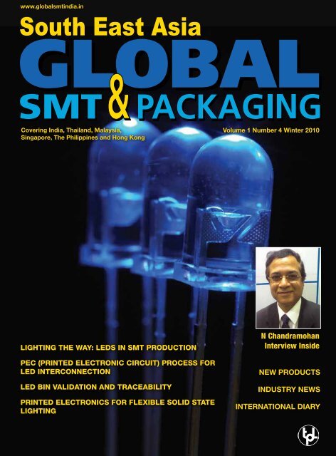
www.globalsmtindia.in<br />
<strong>South</strong> <strong>East</strong> <strong>Asia</strong><br />
Covering India, Thailand, Malaysia,<br />
Singapore, The Philippines and Hong Kong<br />
Lighting the way: LeDs in sMt proDuction<br />
pec (printeD eLectronic circuit) process for<br />
LeD interconnection<br />
LeD bin vaLiDation anD traceabiLity<br />
printeD eLectronics for fLexibLe soLiD state<br />
Lighting<br />
Volume 1 Number 4 Winter 2010<br />
N Chandramohan<br />
Interview Inside<br />
NEW PRODUCTS<br />
INDUSTRY NEWS<br />
INTERNATIONAL DIARY
<strong>South</strong> <strong>East</strong> <strong>Asia</strong><br />
Global SMT & Packaging<br />
is published monthly<br />
by Trafalgar Publications<br />
Limited. The journal is FREE<br />
to qualified professionals and<br />
is available by subscription at a<br />
cost of $380.00 for the current<br />
volume (twelve issues).<br />
Periodicals postage paid at<br />
Rahway NJ. Postmaster send address<br />
corrections to:<br />
Global SMT & Packaging, c/o<br />
Mercury International Limited,<br />
365 Blair Road, Avenel, NJ<br />
07001.<br />
No part of this publication<br />
may be reproduced, stored in<br />
a retrieval system, transmitted<br />
in any form or by any means;<br />
electronic, mechanical, photocopying,<br />
recording or otherwise<br />
without the prior written consent<br />
of the publisher. No responsibility<br />
is accepted for the accuracy of information<br />
contained in the text,<br />
illustrations or advertisements.<br />
The opinions expressed in the<br />
articles are not necessarily those<br />
of the editors or the publisher.<br />
ISSN No. 1474-0893<br />
© Trafalgar Publications Ltd<br />
Designed and Published by<br />
Trafalgar Publications Ltd,<br />
Bournemouth, United Kingdom<br />
With demand growing for LEDs<br />
in electronics, <strong>com</strong>panies in the<br />
SMT industry are expanding their<br />
manufacturing capabilities to meet it.<br />
www.globalsmtindia.in<br />
Contents<br />
2 You’ll be seeing more of us next year<br />
Debasish P. Choudhury<br />
TechNology Focus<br />
10 PEC (printed electronic circuit) process for LED<br />
interconnection<br />
Mike DuBois, Caledon Controls Ltd<br />
14 Printed electronics for flexible solid-state lighting<br />
Marc Chason, Marc Chason and Associates, Inc.<br />
20 LED BIN validation & traceability<br />
Dan Hodgman, Methode Electronics<br />
34 Lighting the way: LEDs in SMT production<br />
Zachery Shook, Count On Tools, Inc.<br />
BusINess Focus<br />
28 What’s the future of the Indian electronics manufacturing<br />
industry?<br />
Pradeep Chakraborty & Usha Prasad<br />
specIal FeaTures<br />
32 Interview—N Chandramohan, Juki India Pvt. Ltd<br />
38 electronica India & productronica India 2010:<br />
Undoubtedly the numero uno business platform in<br />
<strong>South</strong> <strong>East</strong> <strong>Asia</strong><br />
39 10th edition of GlobalTRONICS hosted over 50%<br />
new exhibitors<br />
REgULAR COLUMNS<br />
24 Holiday wishes for a “normal” 2011<br />
Walt Custer and Jon Custer-Topai<br />
10<br />
14<br />
32<br />
Contents<br />
Volume 1, No. 4<br />
OTHER REgULAR<br />
FEATURES<br />
Winter 2010<br />
4 Industry News<br />
40 New Products<br />
46 Association News<br />
48 International Diary<br />
Global SMT & Packaging <strong>South</strong>east <strong>Asia</strong> – Winter 2010 – 1
Editorial<br />
Editorial Offices<br />
Europe<br />
Global SMT & Packaging<br />
Trafalgar Publications Ltd<br />
Unit 18, 2 Lansdowne Crescent<br />
Bournemouth<br />
Dorset BH1 1SA<br />
United Kingdom<br />
Tel: +44 (7766 951665<br />
E-mail: news@globalsmt.net<br />
Website: www.globalsmt.net<br />
United States<br />
Global SMT & Packaging<br />
PO Box 7579<br />
Naples, FL 34102<br />
USA<br />
Tel: +1 (239) 245-9264<br />
Fax: (239) 236-4682<br />
E-mail: news@globalsmt.net<br />
China<br />
Global SMT & Packaging<br />
Electronics Second Research Institute<br />
No.159, Hepin <strong>South</strong> Road<br />
Taiyuan City, PO Box 115, Shanxi,<br />
Province 030024, China<br />
Tel: +86 (351) 652 3813<br />
Fax: +86 (351) 652 0409<br />
Editor-in-Chief<br />
Trevor Galbraith<br />
Tel: +44 7924 581 523 (Europe)<br />
Tel: +1 (239) 245-9264 x101 (US)<br />
E-mail: editor@globalsmt.net<br />
Managing Editor<br />
Heather Lackey<br />
Tel: +1 (239) 245-9264 x105<br />
E-mail: hglackey@globalsmt.net<br />
Editor<br />
Debasish P. Choudhury<br />
Tel: +91 120 6453260<br />
dchoudhury@globalsmtindia.in<br />
Circulation & Subscriptions<br />
Kelly Grimm<br />
Tel: +1 (239) 245-9264 x106<br />
E-mail: subscriptions@globalsmt.net<br />
Advertising<br />
Americas—Derek Laborie<br />
(print & video)<br />
Tel: +1 (239) 245-9264 x102<br />
Mobile: +1 (603) 661-5828<br />
dlaborie@globalsmt.net<br />
Sandy Daneau (digital)<br />
Tel: +1 (239) 245-9264 x104<br />
Cell: +1 (603)-686-3920<br />
sdaneau@globalsmt.net<br />
Europe—Andy Kellard<br />
Tel: +44 7766 951665<br />
akellard@globalsmt.net<br />
<strong>Asia</strong>/Pacific—<br />
Debasish P. Choudhury<br />
Tel: +91 120 6453260<br />
dchoudhury@globalsmtindia.in<br />
Debasish P. Choudhury<br />
Editor<br />
You’ll be seeing more of<br />
us next year<br />
Frankly, “astounding” is the word that best<br />
describes India’s LCD TV sales in October<br />
2010. The total LCD TV shipments<br />
during this one month, which coincided<br />
with the great Indian festival of Diwali,<br />
almost matched up with the total LCD<br />
TV shipments of 2008, when 745,000<br />
LCD TVs were shipped in the entire year.<br />
It seems everyone wanted to erase the<br />
memories of the slowdown days.<br />
As the year draws to a close, we can<br />
feel the excitement in the air. Christmas<br />
parties, vacations and the impending New<br />
Year bashes are the central points of our<br />
discussions now-a-days. Christmas sales,<br />
which a couple of years back were alien<br />
to Indian retail industry, have gained<br />
acceptance due to aggressive consumerism<br />
riding on India’s near 9% GDP growth this<br />
fiscal.<br />
But in this hour of celebration the<br />
biggest shock was the postponement of the<br />
COMPONEX NEPCON India 2010 show,<br />
originally scheduled during mid December<br />
in New Delhi. COMPONEX NEPCON,<br />
which was till 2009 considered to be a<br />
must-attend electronics manufacturing<br />
supply chain show in India, lost its clout<br />
due to Reed Exhibitions’ failure to organise<br />
the show in February 2010. Now, it will<br />
be co-located with the maiden EFY Expo<br />
scheduled in February 2011 in New Delhi.<br />
The interesting aspect of this handshake<br />
is the launch of a brand new trade show<br />
in February 2012 in New Delhi. We will<br />
keenly watch its evolution in the Indian<br />
electronic landscape.<br />
At the same time, it is heartening to<br />
see LED Expo, the only dedicated trade<br />
show for the LED industry in India, to be<br />
held during 3rd week of December in New<br />
Delhi, receive an overwhelming response<br />
from the global LED eco-system. The LED<br />
show will now cover all the standalone<br />
halls in Hall 7 at Pragati Maidan. It once<br />
again shows how favourable government<br />
policies influence businesses around the<br />
world.<br />
At present, all LED chips are imported<br />
from countries such as Japan, Korea,<br />
Germany and the US, and the prices are<br />
high due to low consumption, thereby<br />
prohibiting widespread usage. If we take<br />
into account the current consumer LED<br />
demand projections, the industry estimates<br />
the local manufacturing capacities in India<br />
wouldn’t <strong>com</strong>e up before 2016. But the<br />
real action in the LED industry will <strong>com</strong>e<br />
when the domestic manufacturing scenario<br />
heats up.<br />
Let me share with you an interesting<br />
fact! In 2009, the world produced an<br />
estimated US$ 1,620 billion of electronic<br />
equipment. After the painful recession<br />
of 2009, growth resumed significantly in<br />
2010, with SE <strong>Asia</strong> driving the electronic<br />
equipment rebound, which includes China<br />
& Taiwan. We, at Trafalgar Publications<br />
Ltd. are also buoyed by this feel-good factor<br />
and have decided to increase the frequency<br />
of our magazine next year. In 2011, Global<br />
SMT & Packaging SE <strong>Asia</strong> edition will be<br />
a bi-monthly, with more news, reviews,<br />
interviews, technical articles, columns, etc.,<br />
to increment your desire for manufacturing<br />
technology excellence.<br />
I expect 2011 will be a brilliant year for<br />
Indian electronics industry, and SE <strong>Asia</strong><br />
will continue to drive the growth of the<br />
global electronic equipment production.<br />
Before I conclude, a heartiest ‘Thank<br />
You’ to all our readers, advertisers,<br />
columnists and subscribers for a success<br />
launch of the SE <strong>Asia</strong> edition of Global<br />
SMT & Packaging magazine.<br />
I wish you all Merry Christmas, and a<br />
fantastic New Year 2011!<br />
—Debasish P. Choudhury<br />
2 – Global SMT & Packaging <strong>South</strong>east <strong>Asia</strong> – Winter 2010 www.globalsmtindia.in
Title Industry News<br />
Industry News<br />
Frontline electronics of pune invests in<br />
cyberoptics’ inspection systems<br />
CyberOptics Corporation, a leading SMT<br />
inspection solutions provider, announces that<br />
Frontline Electronics Ltd has purchased its<br />
QX500 and SE350. The systems are scheduled<br />
to be delivered to Frontline’s plant in India in<br />
September 2010.<br />
“We are so pleased to have received this<br />
order from a local leading EMS facility with a<br />
strong <strong>com</strong>mitment to the growth of the Indian<br />
electronics market. This marks a significant<br />
milestone for CyberOptics in India and we are confident that this is the start of a long<br />
relationship with Frontline Electronics,” said Sean Lee, CyberOptics’ <strong>South</strong> <strong>Asia</strong> Sales<br />
Manager. www.frontlineelectronics.<strong>com</strong>, www.cyberoptics.<strong>com</strong><br />
Broad<strong>com</strong> engineer receives<br />
prestigious Ieee alexander graham<br />
Bell Medal<br />
Dr. Arogyaswami Paulraj, who recently<br />
joined Broad<strong>com</strong> Corporation from<br />
Beceem Communications, has been<br />
named the recipient of the Institute of<br />
Electrical and Electronics Engineers’<br />
(IEEE) Alexander Graham Bell Medal, the<br />
organization’s most prestigious honor.<br />
In its award citation, the IEEE’s Board<br />
of Directors said that in its efforts to<br />
recognize “exceptional achievements in our<br />
profession,” Dr. Paulraj was selected “for<br />
pioneering contributions to the application<br />
of multiantenna technology to wireless<br />
<strong>com</strong>munications systems.”<br />
www.broad<strong>com</strong>.<strong>com</strong><br />
element14 offers latest ac/Dc leD<br />
solutions from recoM<br />
element14, formerly known as Farnell<br />
Electronics India (P) Limited, the<br />
industry’s first fusion of <strong>com</strong>merce and<br />
online <strong>com</strong>munity supporting millions of<br />
engineers and purchasing professionals<br />
worldwide, announced the latest addition<br />
of RECOM power solutions, a new range<br />
of high-efficiency constant current LED<br />
drivers in the power range of 12 and 20<br />
Watt to its extensive product portfolio.<br />
With this enhanced offering of cuttingedge<br />
power solutions in the form of a new<br />
range of constant current LED drivers<br />
in the power range of 12 and 20 Watt,<br />
element14 has taken its partnership<br />
with RECOM <strong>Asia</strong> even further to offer<br />
the latest and most innovative solutions<br />
to meet the needs of electronic design<br />
engineers and maintenance and repair<br />
professionals across the <strong>Asia</strong> Pacific.<br />
www.element14.<strong>com</strong><br />
syrma Technology expands<br />
presence in India<br />
Syrma Technology, a Chennai-based<br />
electronics manufacturing services (EMS)<br />
partner, has added a new facility in the<br />
Krishnagiri District of Tamil Nadu,<br />
approximately 110 kilometers from<br />
Bengaluru, India, to ac<strong>com</strong>modate strong<br />
demand for the <strong>com</strong>pany’s custom RFID<br />
tag solutions and its tele<strong>com</strong>munications<br />
infrastructure services. Syrma is the<br />
manufacturing arm of The Tandon<br />
Group, a leader in helping global OEMs<br />
successfully bring products and services to<br />
the fast-growing Indian market. Syrma will<br />
be adding a total of 20,000 square feet of<br />
space and will add approximately 200 jobs<br />
by December. The <strong>com</strong>pany established<br />
the Chennai site in 2006 to provide endto-end<br />
electronics manufacturing services<br />
for the industrial, medical, defense and<br />
tele<strong>com</strong>munications industries.<br />
www.syrmatech.<strong>com</strong>, www.tandongroup.<strong>com</strong><br />
MIrTec europe appoints accurex as<br />
its exclusive distributor for India<br />
MIRTEC appointed Accurex Solutions<br />
Pvt Limited as its exclusive distributor<br />
for India. Accurex brings with them<br />
more than fifteen years’ experience in<br />
sales and service of automatic optical<br />
systems. Accurex is headquartered in<br />
Bangalore and has branches in New Delhi,<br />
Hyderabad, Chennai and Mumbai with<br />
a reputation as one of the best after-sales<br />
service organizations in the Indian market.<br />
With a team of well-trained service and<br />
sales professionals of Accurex and the<br />
unmatched systems of MIRTEC, this<br />
partnership will certainly be a force to<br />
watch. www.mirteceurope.<strong>com</strong>,<br />
www.accurexsolutions.<strong>com</strong>.<br />
cTs incorporates in India to pursue<br />
opportunities in a rapidly growing<br />
eMs market<br />
US-based EMS provider CTS Corporation<br />
has formally incorporated as a business<br />
in India. The new subsidiary, CTS India<br />
Private Limited, located in Haryana, India,<br />
near New Delhi, will allow CTS to operate<br />
with full manufacturing, sales and service<br />
capabilities within India.<br />
CTS has also captured new business for<br />
a customized small engine throttle position<br />
sensor (SETPS) from one of India’s leading<br />
and diversified engine and construction<br />
equipment manufacturers. Production is<br />
expected to begin in the fourth quarter<br />
of 2010 with sales of approximately $2.5<br />
million over its multi-year program life.<br />
www.ctscorp.<strong>com</strong><br />
lg electronics India’s managing<br />
director felicitated with Man of<br />
electronics award<br />
Moon B Shin, managing director, LG<br />
Electronics India, received the “Man<br />
of Electronics” Award during the 31st<br />
annual Consumer Electronics and<br />
Appliances Manufacturers Association<br />
(CEAMA) function. Mr. Shin received<br />
“Man of Electronics” prestigious award<br />
for an outstanding performance and<br />
extraordinary contribution made in the<br />
promotion and development of Indian<br />
Consumer Electronics Industry. LG, which<br />
is the market leader in durable industry,<br />
is today a $2.9 billion <strong>com</strong>pany and is<br />
targeting to achieve $ 10 billion sales by<br />
2015. LG reported year-on-year growth of<br />
30% this year and is confident that the<br />
high demand will last till the remaining<br />
year attributing factors such as rising<br />
in<strong>com</strong>es, positive economic forecasts,<br />
bright job prospects and hence, high<br />
consumer confidence. At the occasion<br />
were present eminent dignitaries including<br />
Dr. Y.V. Verma, president, CEAMA; Mr.<br />
Rajiv Bajaj, hony. secretary, CEAMA; Mr.<br />
Ravinder Zutshi, immediate past<br />
4 – Global SMT & Packaging <strong>South</strong>east <strong>Asia</strong> – Winter 2010 www.globalsmtindia.in
www.globalsmtindia.in<br />
Title<br />
Global SMT & Packaging <strong>South</strong>east <strong>Asia</strong> – Winter 2010 – 5
Industry News<br />
president CEAMA, and P N Dhoot, past<br />
president CEAMA to highlight the recent<br />
developments and observations related to<br />
the industry.<br />
elcoteq Bangalore rewarded in<br />
elcINa-eFy Business excellence<br />
award 2010<br />
Elcoteq’s Bangalore factory has received<br />
the second prize in the “ELCINA-EFY<br />
Business Excellence Award 2010.” The<br />
<strong>com</strong>petition is initiated and organized<br />
by ELCINA (Electronics Industries<br />
Association of India) and EFY (Electronics<br />
for You) to encourage and boost the<br />
innovation culture in the electronics<br />
industry in India.<br />
Elcoteq Bangalore applied for the<br />
Business Excellence -category in the<br />
<strong>com</strong>petition for years 2009-2010, where the<br />
criterion is built on the EFQM model.<br />
India’s mobile phone penetration<br />
to reach 97 percent in 2014, says<br />
isuppli<br />
Cell phone ownership has be<strong>com</strong>e<br />
near ubiquitous in India, with wireless<br />
subscriptions in 2014 expected to amount<br />
to more than 97 percent of the country’s<br />
population of 1.26 billion, according to<br />
the market research firm iSuppli Corp.<br />
By the end of this year, total wireless<br />
subscriptions are projected to reach 766.0<br />
million—45.9 percent higher than the<br />
525.1 million subscribers counted at the<br />
end of 2009, iSuppli mobile industry<br />
forecasts show.<br />
The pace of growth for the future<br />
shows little sign of slackening. Subscriber<br />
numbers will continue to increase<br />
during the next four years, topping the<br />
1 billion mark by 2012. By 2014, mobile<br />
teledensity—a measure of cell phone<br />
availability—likely will reach 97.4 percent<br />
per 100 persons. www.isuppli.<strong>com</strong><br />
DeK continues to partner with<br />
Maxim sMT to capture Indian<br />
market<br />
DEK is extending its partnership with<br />
Maxim SMT in India. Under the<br />
franchise agreement, Maxim SMT will<br />
continue to distribute DEK’s equipment<br />
and manufacture the cutting-edge<br />
VectorGuard® stencils under licence from<br />
DEK, incorporating electroformed foils,<br />
laser-cut nickel foils and plastic stencils,<br />
to meet growing market demands across<br />
India.<br />
Headquartered at New Delhi and<br />
supported by branch offices at Chennai,<br />
Bangalore and Pune, Maxim SMT is<br />
one of the largest SMT <strong>com</strong>panies in the<br />
country and is well positioned to help<br />
manufacturers throughout India gain a<br />
distinct <strong>com</strong>petitive advantage through the<br />
use of DEK’s pioneering stencil system.<br />
In addition, Maxim SMT is well equipped<br />
to support many of DEK’s customers who<br />
have already moved their manufacturing<br />
plants to India. www.dek.<strong>com</strong><br />
asys Technology Days smashes<br />
previous records<br />
Expectations were exceeded as 180<br />
customers and channel partners from<br />
all over the world attended the two-day<br />
program at ASYS Global Headquarters in<br />
Dornstadt, Germany. Visitors were treated<br />
to presentations on new technologies<br />
interwoven with workshops and machine<br />
demonstrations. The highlights include the<br />
launch of a new “INSIGNUM” family of<br />
laser markers, which utilizes the <strong>com</strong>pany’s<br />
research in the area of lasers and includes<br />
four machines types from basic to<br />
advanced flexible high speed units.<br />
Additionally, new Laser Depaneling<br />
machines were introduced coupled with<br />
new flexible options for mechanical<br />
routers. In the area of new technologies,<br />
the <strong>com</strong>pany unveiled its plans for<br />
the LED market segment with a new<br />
Singulation System that replaces the<br />
traditional sawing process. www.asys-group.<br />
<strong>com</strong><br />
Koh young’ ceo, Dr. Kwangill Koh,<br />
receives south Korean government<br />
award<br />
Dr. Kwangill Koh, founder and CEO and<br />
president of 3D inspection technology<br />
leader Koh Young, was recently honored<br />
by the government of <strong>South</strong> Korea,<br />
and Korean industry leaders, for his<br />
achievements in making his <strong>com</strong>pany<br />
a dominant force among technology<br />
<strong>com</strong>panies both domestically and globally.<br />
Awarded by the government of <strong>South</strong><br />
Korea, the Tin Tower Order of Industrial<br />
Service Merit—The Best Venture Company,<br />
recognized Dr. Koh for his outstanding<br />
contribution to the government’s<br />
industrial development and contributions<br />
to the Korean economy. The medal was<br />
presented to Dr. Koh in ceremonies on<br />
October 19, 2010. The award recognized<br />
that “Kwangill Koh, the CEO of Koh<br />
Young Technology, Inc., highly contributed<br />
to increased <strong>com</strong>petitive advantages of<br />
Korea by providing the first high-speed<br />
3D inline solder paste inspection systems<br />
to worldwide electronics manufacturers.”<br />
www.kohyoung.<strong>com</strong><br />
Bridgestone, Delta electronics to<br />
develop next-generation electronic<br />
paper products<br />
Bridgestone Corporation and Delta<br />
Electronics of Taiwan entered into<br />
a joint agreement to develop and<br />
manufacture the next generation<br />
of electronic paper products and<br />
applications. The development will<br />
provide valuable synergies between<br />
Bridgestone’s Quick Response Liquid<br />
Powder Display (QR-LPD) technology<br />
and Delta’s core <strong>com</strong>petencies in the<br />
areas of energy solutions and imaging<br />
technology. QR-LPD is a bistable, reflective<br />
display technology that uses airborne,<br />
electronically switchable powder particles<br />
of extremely high fluidity. The results are<br />
paper-like visibility, wide viewing angles,<br />
fast response times and ultra-low power<br />
consumption. www.deltaww.<strong>com</strong><br />
Test advantage hardware<br />
announces new director of sales for<br />
the asia pacific region<br />
Test Advantage Hardware, LLC, a newly<br />
acquired subsidiary of Boston Semi<br />
Equipment, LLC (BSE Group), has hired<br />
Richard Huang as director of sales for<br />
the <strong>Asia</strong> Pacific region. Huang will focus<br />
on expanding the Arizona, U.S.-based<br />
<strong>com</strong>pany’s leasing portfolio and supporting<br />
the growth of its hardware sales business<br />
throughout <strong>Asia</strong>.<br />
“The <strong>Asia</strong> Pacific region continues to<br />
experience strong growth across a broad<br />
spectrum of equipment requirements,”<br />
said Colin Scholefield, executive vice<br />
president of the BSE Group.<br />
www.testadvantage.<strong>com</strong>, www.bsegroup.<strong>com</strong><br />
Nexray of singapore wins the B.I.D.<br />
International star award for Quality<br />
in geneva<br />
Nexray Pte Ltd, a leading electronics<br />
manufacturing technology solutions<br />
<strong>com</strong>pany based in Singapore, received the<br />
B.I.D International Star Award for Quality<br />
at the 35th International Star Award for<br />
Quality (ISAQ) Convention in Geneva on<br />
6th September 2010. B.I.D. International<br />
Star Award for Quality includes a trophy<br />
that B.I.D. presents to those <strong>com</strong>panies<br />
from around the world that best adhere<br />
to excellence and innovation in their<br />
practices, putting quality first.<br />
The <strong>com</strong>panies awarded at the<br />
gathering in Geneva were distinguished<br />
not only for their business success,<br />
but for their dedication to continuous<br />
improvement, abiding by the principles of<br />
the B.I.D.-created QC100 model of Total<br />
Quality Management. www.nexray.biz<br />
6 – Global SMT & Packaging <strong>South</strong>east <strong>Asia</strong> – Winter 2010 www.globalsmtindia.in
www.globalsmtindia.in<br />
Title<br />
Global SMT & Packaging <strong>South</strong>east <strong>Asia</strong> – Winter 2010 – 7
Industry News<br />
8 – Global SMT & Packaging <strong>South</strong>east <strong>Asia</strong> – Winter 2010 www.globalsmtindia.in
www.globalsmtindia.in<br />
Title<br />
Global SMT & Packaging <strong>South</strong>east <strong>Asia</strong> – Winter 2010 – 9
PEC (printed electronic circuit) process for LED interconnection<br />
PEC (printed electronic<br />
circuit) process for LED<br />
interconnection<br />
Mike DuBois, Caledon Controls Ltd., Mississauga, Ontario, Canada<br />
PCB mounting of LEDs<br />
has to date been limited to<br />
mechanical interconnection<br />
or the use of printed circuits<br />
boards built on thermally<br />
conductive copper clad<br />
aluminum substrates. This<br />
paper discusses the use of<br />
enhanced thermally conductive<br />
inks for LED interconnection.<br />
Keywords: Adhesives, Packaging,<br />
Modified Polycarbamin Acid<br />
Derivates, mCD<br />
Higher wattage LEDs/power <strong>com</strong>ponents<br />
or their placement in higher densities<br />
requires a larger dissipation of heat in a<br />
more effective way.<br />
The following is quoted from Canadian<br />
Electronics magazine:<br />
“With rapid advancements in power<br />
reduction, and minimizing and<br />
controlling LED heat, it is expected<br />
that future applications will use<br />
less-expensive, rigid aluminum-backed<br />
printed circuit boards for proper heat<br />
dissipation and move towards more<br />
cost-effective flexible circuits. This is<br />
also being driven by signal and display<br />
applications, where most of the future<br />
LED growth is expected.”<br />
—Gijs Werner, FCI<br />
PCB mounting of LEDs has to date been<br />
limited to mechanical interconnection<br />
or the use of printed circuits boards built<br />
on thermally conductive copper clad<br />
aluminum substrates.<br />
These laminated substrates which are<br />
available from several specialty laminate<br />
manufacturers, typically consist of a copper<br />
foil that is laminated to the aluminum<br />
using a glass cloth impregnated with<br />
heat conducting additive filled epoxies.<br />
The cloth offers small window openings<br />
between the weave patterns where the filled<br />
epoxies can make contact with the both the<br />
Figure 1. Copper clad aluminum substrate.<br />
copper foil and the aluminum to transfer<br />
heat. The glass cloth, which <strong>com</strong>prises 50<br />
percent of the prepreg, significantly reduces<br />
the thermal conductivity. Additionally,<br />
the existing available thermal prepregs are<br />
thicker at 100 microns (.004 mils), which<br />
increases the effective thermal resistance<br />
limiting the maximum watts per square<br />
inch dissipation.<br />
A printed circuit board manufacturer<br />
would employ this laminate material,<br />
laminating photo-imageable etch resist,<br />
exposing with UV light then developing<br />
to form a circuit image, then etching away<br />
unwanted copper to produce circuit traces.<br />
All exposed aluminum must also be well<br />
masked off, a time- and material-consuming<br />
task.<br />
printed electronic inks<br />
Enhanced thermally conductive inks are<br />
much more versatile.<br />
They can be used to make a more<br />
Figure 2. Etched copper circuit trace on thermal dielectric & actual etched circuit; 60X.<br />
10 – Global SMT & Packaging <strong>South</strong>east <strong>Asia</strong> – Winter 2010 www.globalsmtindia.in
efficient thermally conductive copper<br />
clad aluminum laminate substrate by the<br />
PCB fabricator themselves (Figure 1) or<br />
could used by selectively printing both the<br />
dielectric and conductive traces to make<br />
a thermally conductive circuit by anyone<br />
with a silk screen printer and a thermal<br />
oven (See Figure 3).<br />
Using CCD-120A thermally conductive<br />
dielectric ink with its nano technology<br />
enhanced formulation in making<br />
PCB boards or even making copper clad<br />
aluminum circuit laminate will deliver<br />
lower thermal resistance than that of other<br />
currently available copper clad aluminum<br />
substrates.<br />
copper-clad aluminum<br />
The thermally conductive B-stage ink<br />
is applied to the surface of either the<br />
copper foil or the aluminum and is semi<br />
cured (B-Stage) using a thermal oven.<br />
Application is typically a silk screening<br />
operation to deposit a thin film of thermal<br />
ink approximately .001” thick. The ink is<br />
then baked at 250˚F for 20-30 minutes, at<br />
which time the material reaches the desired<br />
Figure 4. Heat radiating <strong>com</strong>parison.<br />
www.globalsmtindia.in<br />
B-stage cure.<br />
The coated B-stage aluminum is laminated<br />
with the copper foil of choice using a<br />
typical vacuum-assist laminating press and<br />
fully cured under pressure.<br />
The end result is a thin layer only<br />
25 microns thick of the thermal material<br />
sandwiched between the copper and<br />
aluminum. With this version of a copper<br />
clad aluminum, the B stage thermal ink<br />
offers lower thermal resistance, because<br />
the surface area contact and the thickness<br />
of the deposit. As well, the pressure<br />
of the lamination cycle constricts the ink<br />
allowing a closer contact between thermally<br />
conductive ceramic particles increasing the<br />
thermal conductance. A one mil thick layer<br />
of thermal ink properly applied has a 2500<br />
volt rating.<br />
Processing the panel to make a<br />
simple single-sided circuit is a done by the<br />
time-honored “print and etch” method<br />
requiring PCB fabrication equipment and<br />
wastewater treatment facilities because of<br />
the copper etching process.<br />
Figure 2 shows the etched circuit trace<br />
paths on the Thermally Conductive dielec-<br />
PEC (printed electronic circuit) process for LED interconnection<br />
Figure 3. Silver trace on selective print thermal<br />
dielectric.<br />
tric. Adhesion to aluminum with our 2 w/<br />
mc ink is excellent; the thermal dielectric<br />
has a hard surface due to its high ceramic<br />
content but can accept a coat of soldermask<br />
before the final cure. A <strong>com</strong>patible<br />
solder mask could later be applied.<br />
print-only circuits<br />
A selectively deposited thermal conductive<br />
ink on the aluminum offers the benefit of<br />
being deposited only where thermal heat<br />
transfer is needed, reducing consumables<br />
costs when <strong>com</strong>pared to the currently<br />
popular copper clad aluminum substrate,<br />
which has full coverage of the underlying<br />
surface with the glass cloth impregnated<br />
with heat conductive material.<br />
The circuit traces are screened on<br />
Global SMT & Packaging <strong>South</strong>east <strong>Asia</strong> – Winter 2010 – 11
PEC (printed electronic circuit) process for LED interconnection<br />
Figure 5. PECs developed LPI dielectric. Figure 6. PEC 4 mil lines/space flush silver.<br />
using new nano silver solderable inks. The<br />
net result is that by using a thermal ink<br />
selectively applied under the silver traces,<br />
less of the thermal material is used per<br />
the same overall area yet will deliver better<br />
heat transfer capability because it is thinly<br />
applied.<br />
Building a printed circuit utilizing the<br />
print-only process can not only simplify the<br />
manufacturing, but it will reduce its costs.<br />
Print-only is manufactured with a full additive<br />
green technology that will in the end<br />
deliver better heat transmission performance.<br />
No etching equipment is required.<br />
print only<br />
Printing the thermal dielectric ink<br />
selectively where needed and then printing<br />
electrically conductive traces on top the<br />
thermal dielectric with low resistance<br />
Figure 6. PEC 4 mil lines/space flush silver.<br />
silver ink reduces costs, as the dielectric is<br />
applied only where needed (Figure 3).<br />
Screen printing a slightly wider surface<br />
area than that of the conductors, then curing<br />
the dielectric at a temperature of 250˚F<br />
for 30 minutes establishes a non-tacky but<br />
yet uncured surface, which is then overprinted<br />
with the silver conductive traces.<br />
The silver ink is then cured at 150˚C for<br />
30 minutes, which fuses the silver trace<br />
into a solid metal track. A <strong>com</strong>patible<br />
solder mask can be applied and tack dried,<br />
followed by an overall full en<strong>com</strong>passing a<br />
cure of 300˚F for 60 minutes, which forms<br />
the final circuit. Using thermal/silver ink<br />
<strong>com</strong>binations offers many more build options<br />
and cost concession possibilities.<br />
As there is no requirement to etch<br />
and therefore no need to mask off the<br />
aluminum when etching or processing,<br />
labor is tremendously reduced.<br />
When utilizing the silver ink trace<br />
technology, assembling and soldering the<br />
<strong>com</strong>ponents requires a lower temperature<br />
solder which is typically used in assembly<br />
houses.<br />
The thermal characteristics are vastly<br />
improved over that of a normal copperclad<br />
aluminum etched type circuit. The<br />
area of the aluminum that is not covered<br />
by the dielectric material and silver traces<br />
has a larger thermal conductance (380 w/<br />
mc) than the aluminum with a layer of 2<br />
w/mc thermal material.<br />
Figure 4 shows a <strong>com</strong>parison between<br />
three heat conducting and dissipating<br />
constructions. Clearly evident is the larger<br />
amount of exposed aluminum made possible<br />
with an all printed version of the<br />
board and the resulting superior heat dis-<br />
12 – Global SMT & Packaging <strong>South</strong>east <strong>Asia</strong> – Winter 2010 www.globalsmtindia.in
sipation available.<br />
printed electronics versatility<br />
Using ink technology, more <strong>com</strong>plex<br />
circuit boards can be manufactured by<br />
using the more advanced and “green” PEC<br />
technologies described below.<br />
Thermally conductive PEC process<br />
Silk-screen-coating the aluminum with<br />
thermally conductive dielectric, a second<br />
layer of a specially formulated LPI<br />
dielectric ink is deposited at some 1 to<br />
1.2 mil thickness depending on screen<br />
mesh selections. If desired, extra layers<br />
of the dielectric will provide for thicker<br />
conductor lines.<br />
Tack-cured and then exposed using<br />
ordinary UV exposure units, the LPI is<br />
spray developed on typical developing<br />
equipment and chemistry. What remains<br />
is a coating on the substrate with trenches<br />
and pad openings (Figure 5).<br />
A thermally conductive PEC’s third<br />
<strong>com</strong>ponent is a nano technology silver conductive<br />
ink that is applied onto the surface<br />
of the LPI. Filling of the trenches and pads<br />
is ac<strong>com</strong>plished and the conductive ink is<br />
cured. The ink fuses into a solid mass with<br />
a slight deposit on the surface of the LPI,<br />
which is easily removed (Figure 6).<br />
The next step is a repeat of the second,<br />
except that this interconnection layer will<br />
be a via formation layer only. Coat, tack,<br />
expose, develop and silver fill.<br />
Because the LPI is never stripped off<br />
and the entrenched silver conductive ink<br />
is level with the top of the LPI, everything<br />
conductive is flush to the dielectric.<br />
The same process is repeated again for<br />
the second conductive layer.<br />
The result is that the interconnect<br />
“vias” are buried, and there is a 100%<br />
metal connection to the first layer. In the<br />
end, anything reliability-wise to a PCB<br />
PTH interconnect has been eliminated.<br />
The process is repeated for as many<br />
layers as is required by design. The last top<br />
layer has pads left exposed for <strong>com</strong>ponent<br />
mounting. All circuitry and interconnections<br />
are buried.<br />
Versatile, boards can be configured to<br />
use the PEC full additive process even on<br />
two sides of the aluminum if desired or<br />
build multilayer circuits all on one side of<br />
the aluminum backing.<br />
Figure 7 shows a typical PEC build<br />
configuration: A multilayered, single-sided<br />
thermally conductive PEC technology<br />
PCB. Designs could be altered a number<br />
of ways, allowing many new interconnect<br />
possibilities.<br />
www.globalsmtindia.in<br />
conclusion<br />
In summary, using printed electronic ink<br />
products and processes to manufacture<br />
high performance thermally conductive<br />
circuit boards offers clear advantages in<br />
manufacturing flexibility, performance and<br />
cost.<br />
When using these inks in the full additive<br />
print only process or the PEC method,<br />
these high performance heat-dissipating<br />
circuits are also environmentally friendly.<br />
PEC (printed electronic circuit) process for LED interconnection<br />
Mike is an industry veteran going back to<br />
military board manufacturing using shoe eyelets<br />
for interconnection of layers. Joining the ranks<br />
of Caledon Controls, a growing distribution<br />
firm, Mike is involved in diversification efforts<br />
and searching for alternative PCB processing<br />
methods.<br />
Global SMT & Packaging <strong>South</strong>east <strong>Asia</strong> – Winter 2010 – 13
Printed electronics for flexible solid-state lighting<br />
Printed electronics for flexible<br />
solid-state lighting<br />
Marc Chason, Marc Chason and Associates, Inc., Schaumburg, Illinois, USA<br />
Printed electronics technologies<br />
are being introduced as<br />
<strong>com</strong>petitors to crystalline<br />
semiconductor technologies in<br />
several applications, including<br />
logic circuits, photovoltaic<br />
cells and light emitting diodes<br />
(LED). Near term solidstate<br />
lighting (SSL) products<br />
based on LED technologies<br />
are entering the general<br />
illumination market. These<br />
SSL products use conventional<br />
SMT processes in a four-level<br />
assembly hierarchy to fabricate<br />
light engines for incorporation<br />
into luminaires. In parallel<br />
with LED device development,<br />
printed electronics technologies<br />
are also moving forward using<br />
ink-based systems to fabricate<br />
organic-LEDs (OLED).<br />
However, the OLED assembly<br />
hierarchy used to fabricate<br />
light emitting structures is<br />
significantly different from<br />
that for LED-based devices.<br />
This paper will <strong>com</strong>pare<br />
LED and printed OLED<br />
assembly technologies, discuss<br />
available printing technologies<br />
and ink systems for OLED<br />
structures and address OLED<br />
fabrication and assembly<br />
issues.<br />
Keywords: Solid State Lighting,<br />
SSL, OLED<br />
This paper was originally presented at<br />
SMTAI International 2010 in Orlando,<br />
Florida.<br />
Introduction<br />
By various estimates, lighting is one of the<br />
largest U.S. consumers of electrical power 1 .<br />
Around the world, significant economic<br />
and environmental pressures are driving<br />
major energy saving efforts with respect<br />
to lighting technology. One area receiving<br />
a great deal of attention for replacing<br />
general lighting sources, i.e., incandescent<br />
lamps, fluorescent lamps and <strong>com</strong>pact<br />
fluorescent lamps (CFL), is Solid State<br />
Lighting (SSL). The excitement with SSL<br />
arises from the rapid performance increase<br />
demonstrated by crystalline LED-based<br />
lighting technology.<br />
Globally, industrial investments<br />
and government funded activities are<br />
supporting R&D and manufacturing<br />
development. The result has been<br />
SSL lamp performance that in some<br />
cases is equal to or better than existing<br />
incandescent and fluorescent lamps. LEDbased<br />
lamps are now <strong>com</strong>mercially available<br />
and in many cases is cost <strong>com</strong>petitive with<br />
incandescent and fluorescent lighting<br />
systems based on life-cycle assessments.<br />
Furthermore, the long lived SSL product<br />
can produce additional cost savings<br />
through reduction of maintenance costs.<br />
Following Holonyak’s 2 1962<br />
announcement of the first light-emitting<br />
diode, LED efficacy has dramatically<br />
increased over time, Figure 1 3 . Efficacy,<br />
the ratio between the amount of light<br />
that a source generates relative to its<br />
energy input, is measured in lumens<br />
per watt, (lm/W). During this time, the<br />
incumbent incandescent lamp efficacy has<br />
plateaued at a relatively low level. While<br />
the various fluorescent technologies have<br />
demonstrated increased efficacy, their<br />
growth has not been as rapid as that for the<br />
LEDs.<br />
In addition to increased performance,<br />
LED cost has rapidly decreased. Haitz’s<br />
Law (Figure 2), analogous to Moore’s Law<br />
for ICs, demonstrates how the cost of LED<br />
lighting decreases (cost per lumen) while<br />
the efficacy increases (lumens per watt)<br />
over time 4 . Note that the “flux/package”<br />
trend is increasing faster than the historical<br />
trend.<br />
Organic-LED (OLED) is also<br />
undergoing rapid development, but<br />
is several years behind the LED-based<br />
technology. In contrast to point source<br />
LED luminaires, OLED products are<br />
dispersed light sources, which promise<br />
Level Assembly Step Comments<br />
3 System level assembly Luminaire assembly<br />
Product is sold to end customer<br />
2 Package on board Light Engine—SMT assembly processes<br />
1 LED in package Light Engine—SMT assembly processes<br />
0 LED Device Light Source—Focuses on LED fabrication at the<br />
wafer level<br />
Table 1. LED assembly hierarchy.<br />
Level Assembly Step Comments<br />
3 System level assembly Assembly of luminaire<br />
Product is sold to end customer<br />
2 Interconnects, leads & packaging<br />
1 OLED Device Integration with R2R processes<br />
0 Focuses on printing/vapor deposition of OLED<br />
Table 2. OLED assembly hierarchy.<br />
14 – Global SMT & Packaging <strong>South</strong>east <strong>Asia</strong> – Winter 2010 www.globalsmtindia.in
Figure 1. Historical and predicted light source efficacies. Figure 2. 2010 version of Haitz’s Law.<br />
new lighting paradigms. Developed by<br />
Kodak 5 in the 1980s, OLED devices were<br />
initially fabricated using vapor deposition<br />
processes. The opportunity to use printing<br />
processes for OLED fabrication opens up<br />
new opportunities.<br />
Presently, OLED efficacy is lower<br />
than that for LED product, but is rapidly<br />
increasing. It is too soon to know whether<br />
OLED products will follow Haitz’s Law.<br />
ssl assembly hierarchies<br />
LED assembly<br />
LED-based SSL assembly follows a 4 level<br />
assembly hierarchy, Table 1.<br />
LED assembly uses a broad range of<br />
SMT processes and unique materials.<br />
Following die singulation and lightemission<br />
testing, binned die (based on<br />
light quality) are assembled into a light<br />
source. A Level 1 LED assembly is depicted<br />
in Figure 3 6 . Ultimately, the light engine is<br />
Figure 3. Level 1 LED package assembly.<br />
www.globalsmtindia.in<br />
placed in a luminaire.<br />
OLED assembly<br />
In contrast to LED assembly, OLED<br />
assembly follows a very different assembly<br />
process, Table 2. While this is still a<br />
four-level assembly hierarchy, Levels 0, 1<br />
and 2 are merged into a <strong>com</strong>prehensive<br />
assembly step since OLED fabrication<br />
intrinsically produces the light source<br />
(Level 0), and light engine (Level 1 and 2)<br />
in an interrelated process, not as a series of<br />
discrete assembly steps, which defines LED<br />
SSL assembly.<br />
This OLED assembly hierarchy<br />
arises from the nature of the OLED<br />
device, which is different from that for a<br />
crystalline based LED. A typical OLED<br />
light source fabricated on a glass substrate,<br />
shown in Figure 4 7 , is <strong>com</strong>posed of a<br />
stack of thin films (usual total thickness<br />
of 100-200 nm) situated between planar<br />
Printed electronics for flexible solid-state lighting<br />
electrodes, with at least one transparent<br />
electrode to enable light to exit the OLED<br />
structure. Descriptions of the various layers<br />
are described in Table 3.<br />
Visible light is created when electrons<br />
and holes, driven by an applied voltage<br />
across the electrodes, <strong>com</strong>bine in the<br />
OLED layers. A luminaire is formed when<br />
the OLED is assembled into a structure<br />
that protects the OLED from physical and<br />
environmental damage as well as supplying<br />
it with electrical energy and control<br />
functions.<br />
SSL OLED technology began as<br />
a display technology. In addition to<br />
developing the materials and fabrication<br />
processes to produce displays, lithography<br />
capable of sub-millimeter resolution was<br />
also required for forming small pixels with<br />
the OLED material sets. While requiring<br />
similar OLED materials and substrates,<br />
SSL requires lower resolution lithography<br />
(i.e., the pixels are larger) so that a critical<br />
display manufacturing step is removed<br />
from the lighting path. The result is a<br />
significant fraction of the manufacturing<br />
cost is reduced for a luminaire relative to<br />
a display, while concurrently increasing<br />
manufacturing throughput and yields.<br />
oleDs for solid-state lighting<br />
As noted in the OLED assembly hierarchy,<br />
Levels 0, 1 and 2 are strongly interrelated.<br />
This interrelation is made more <strong>com</strong>plex<br />
by multiple options available for producing<br />
the OLED device. These include:<br />
• Vapor deposition vs. printed<br />
processes<br />
• Flexible substrate vs. rigid substrate<br />
• Reel-to-reel (R2R) vs. sheet fed<br />
processing<br />
While some OLED material systems can be<br />
Global SMT & Packaging <strong>South</strong>east <strong>Asia</strong> – Winter 2010 – 15
Printed electronics for flexible solid-state lighting<br />
Figure 4. Assembly structure for OLED-based device.<br />
vapor deposited, this paper will generally<br />
focus on those technologies that use<br />
printing technologies for fabricating the<br />
OLED. We will discuss vapor deposited<br />
processes for <strong>com</strong>parison purposes.<br />
OLED materials have a rich<br />
developmental history which is described<br />
in other publications 8 . The materials span<br />
multiple spaces of the OLED fabrication<br />
process and continue to undergo rapid<br />
development. This development is<br />
intimately tied to the chosen deposition<br />
process and substrate properties.<br />
Furthermore, these processes are strongly<br />
correlated with the associated ink<br />
technology.<br />
Figure 5. Vertically stacked OLED structures for<br />
producing white light.<br />
OLED light emitting material systems<br />
Printable OLED inks are available from<br />
a number of <strong>com</strong>mercial suppliers.<br />
Polymer OLED materials (polymer light<br />
emitting diode, or PLED) are a class of<br />
polymers that emit light and are solution<br />
proccesable. Alternatively, vacuum thermal<br />
processes are typically used to deposit small<br />
molecule OLED (SMOLED) materials.<br />
In addition to the light emitting<br />
materials that form the OLED PN<br />
junction, additional materials are used<br />
to enhance OLED performance. For<br />
example, inks have been developed for<br />
Hole Transport and Electron Transport<br />
functions.<br />
LED-based solid-state lighting produces<br />
white light by mixing light from red, green<br />
and blue LEDs, or by using phosphors<br />
to convert blue or UV LED light to<br />
white light. Similar schemes can be used<br />
with OLED devices. Various OLED<br />
constructions have been developed to<br />
realize white light sources. Figure 5 shows a<br />
vertically stacked “hybrid tandem” OLED<br />
structure for producing white light 9 , where<br />
the OLED structures are deposited on top<br />
of each other. Light is produced in the<br />
two junction regions and exits the OLED<br />
through the transparent anode side. An<br />
alternative structure that spreads the light<br />
emitting structures along the substrate is<br />
depicted in Figure 6 10 .<br />
Figure 6. Horizontally positioned OLED structures<br />
for producing white light.<br />
Layer Function<br />
Metal Cathode Low work function material<br />
Electron Transport Layer Transport electrons to organic emitters;<br />
block hole transport<br />
Organic Emitters Electron/hole re<strong>com</strong>bination and light<br />
emission<br />
Hole Injection Layer Transport holes to organic emitters;<br />
block electron transport<br />
Anode Transparent conductor<br />
Glass Substrate<br />
Table 3. Description of OLED Layers (from Figure 4).<br />
In the horizontally arranged OLED<br />
structures, the red, green and blue light<br />
sources are positioned next to each other<br />
rather on top of each other. This reduces<br />
the number of vertical layer depositions.<br />
OLED substrate material systems<br />
The OLED light emitting structures are<br />
encased between two electrodes, one of<br />
which needs to be transparent so that<br />
the generated light can exit the OLED<br />
structure. The transparent electrode is<br />
usually the anode. Rigid OLED devices<br />
are typically fabricated on glass coated<br />
with a transparent conductive oxide<br />
(TCO), usually Indium Tin Oxide (ITO).<br />
Flexible anodes are fabricated on polymer<br />
substrates similarly coated on one side with<br />
ITO. PET (polyethylene terephthalate) and<br />
PEN (polyethylene naphthalate) polymers<br />
have been used for substrates. The cathode<br />
is typically a low work function metal foil,<br />
for example aluminum or calcium.<br />
OLED light emitting materials are<br />
extremely sensitive to water vapor and<br />
oxygen. For <strong>com</strong>mercial devices 11 , typical<br />
water vapor transmission rates (WVTR)<br />
are
emaining following assembly.<br />
Light extraction from the OLED device<br />
is a primary concern for increasing OLED<br />
panel efficiency and luminaire efficacy. In<br />
conventional OLEDs, it is estimated that<br />
only 20% of the generated light exits the<br />
OLED due to refractive index mismatch 12 .<br />
Films that redirect light between the<br />
substrate and the electrode can be used to<br />
enhance light output. Photonic crystals can<br />
provide improved coupling to enable light<br />
to exit the OLED.<br />
OLED printing processes<br />
SMT assembly makes use of various<br />
printing and deposition processes in the<br />
production of electronic products, e.g.,<br />
solder paste screen printing, conformal<br />
coating, conductive adhesive dispensing,<br />
etc. Printing technologies for OLED<br />
technology embrace a number of printing<br />
technologies that move beyond the typical<br />
SMT space. The ability to print many of<br />
the materials that <strong>com</strong>prise an OLED SSL<br />
device makes such fabrication a <strong>com</strong>pelling<br />
value proposition.<br />
The OLED substrate will determine<br />
whether R2R or sheet fed processes will<br />
be feasible. Rigid glass substrate systems<br />
require sheet fed processes, while flexible<br />
substrates such as polymer and metal<br />
foils can be used with either process.<br />
While R2R printing produces long sheets<br />
of OLED material the OLED devices<br />
still need to be excised from the web.<br />
Depending upon the manufacturing<br />
flow and subsequent processing steps,<br />
sheet fed printing that produces near-net<br />
final shapes may be as cost effective as<br />
R2R printing with its subsequent slitting<br />
and excising steps. Engineering analysis<br />
is required to determine the optimum<br />
system.<br />
OLED printing techniques can be<br />
differentiated by the method they use to<br />
feed the substrate to the printing process.<br />
R2R processes print on long continuous<br />
material films, while sheet fed printing<br />
uses individual sheets in discrete sizes.<br />
Relative to sheet fed processes, R2R<br />
processes minimize the load/un-load time<br />
between printing stations. However, sheet<br />
fed processes can be made to mimic R2R<br />
printing with inline techniques.<br />
A simplified R2R process flow for<br />
producing an OLED light source is<br />
depicted in Figure 7 13 . In this schematic<br />
diagram, the transparent substrate is<br />
printed with the anode layer and then<br />
successive layers of functional inks are<br />
in-line printed to produce the OLED<br />
structure. For white light production,<br />
red, green and blue emissive layers can<br />
www.globalsmtindia.in<br />
Figure 7. Schematic of a R2R OLED printing<br />
process.<br />
Figure 9. Left—Osram ORBEOS product. Right—Philips Lumiblade product.<br />
be printed, but if a single light color is<br />
required then only printing that ink would<br />
be necessary. White light can also be<br />
produced by printing a blue light emissive<br />
layer and adding a phosphor layer that<br />
converts the blue light to white light,<br />
which is similar to crystalline LED SSL<br />
practices. Within this basic process flow<br />
numerous permutations are possible to<br />
address cost effective manufacturing. The<br />
encapsulation and <strong>com</strong>pleted module steps<br />
will be discussed in later sections.<br />
Gravure, flexographic and slot-die<br />
coating processes can be used to print or<br />
coat the inks to produce an OLED device.<br />
An alternative to these printing processes<br />
are inkjet printing processes. While the<br />
first three processes require contract<br />
between dispensing equipment and the<br />
substrate, inkjet printing is a non-contact<br />
process. Inkjet printing processes have<br />
been developed for fabricating OLED<br />
displays 14 , Figure 8. An OLED suitable<br />
for SSL applications could be simpler to<br />
produce since it would not require the<br />
polysilicon TFT and the pixel sizes could<br />
be larger.<br />
Screen-printing technology (which<br />
is an SMT staple) uses a masked screen<br />
to determine the location where the ink<br />
will be deposited. With both flat bed<br />
and rotary machines available, it has<br />
wide applicability because it can print<br />
on many types of surfaces and substrates<br />
Printed electronics for flexible solid-state lighting<br />
Figure 8. Schematic of an inkjet OLED printing<br />
process.<br />
and is <strong>com</strong>patible with a wide range of<br />
ink viscosities. It is suitable for printing<br />
relatively thick layers to produce electrical<br />
conductors and dielectric layers. These<br />
are required: a) to produce interconnects<br />
between the OLED light engine and power<br />
sources, b) to generate printed bus bars to<br />
bring electrical power to the OLED pixels,<br />
c) to provide conductors for control lines<br />
to offer unique features and d) to provide<br />
insulating layers where appropriate. Bus<br />
bars and interconnect conductors can be<br />
formed from silver or carbon inks. Silver<br />
inks have higher conductivity while carbon<br />
is lower cost. Bus bars and interconnect<br />
lines must be positioned so that they offer<br />
the lowest shadowing effects.<br />
OLED encapsulation processes<br />
In an OLED SSL device, the OLED light<br />
source generates the light (Assembly Level<br />
1 and 2) while the light engine (Assembly<br />
Level 2) enables it to couple to the<br />
luminaire. Assembly Level 2 must provide<br />
the light engine environmental protection<br />
(e.g., humidity resistance, oxygen<br />
resistance, etc.) and physical protection<br />
(e.g., abrasion resistance, etc.). Assembly<br />
Level 2 also provides the opportunity for<br />
improving light extraction.<br />
Printed OLEDs are thin structures<br />
with electrodes on the top and bottom<br />
surfaces. Since the separation distance<br />
between the electrodes is small and the<br />
Global SMT & Packaging <strong>South</strong>east <strong>Asia</strong> – Winter 2010 – 17
Printed electronics for flexible solid-state lighting<br />
Figure 10. Cross section of Philips Lumiblade device. Figure 11. Schematic diagram of GE lamination process for OLED fabrication.<br />
flexible substrate materials tend to be<br />
soft, care must be taken when cutting<br />
and excising OLED devices from the web.<br />
Electrode surfaces cannot <strong>com</strong>e in contact<br />
with each other (e.g. due to edge smearing)<br />
since they would generate an electrical<br />
short and cause device failure. Mechanical<br />
cutting tools or cutting lasers can be used<br />
if they don’t leave burrs.<br />
Encapsulation of OLED light<br />
engines via hermetic barriers is highly<br />
advantageous to ensure long product<br />
lifetime. Most barrier systems follow a<br />
multilayer approach. Laminate films<br />
are <strong>com</strong>prised of thin polymer layers<br />
interspersed with thin ceramic layers<br />
to provide hermeticity and maintain<br />
flexibility. Coating processes also use a<br />
multilayer approach with the hermetic film<br />
built up with polymer layers and ceramic<br />
layers.<br />
Numerous <strong>com</strong>panies are developing<br />
barrier films that can be applied via<br />
printing/coating or film lamination<br />
processes. In addition to offering<br />
protection against water vapor and<br />
oxygen, these encapsulation layers must<br />
also offer abrasion resistance and provide<br />
physical protection to the light engine. If<br />
they can’t supply these attributes within<br />
one barrier film, then additional layers<br />
need to be applied that meet the product<br />
requirements.<br />
OLED device surfaces have a higher<br />
Figure 12. Example of printed flexible OLED<br />
devices.<br />
refractive index than air, which coupled<br />
with a planar emitting surface leads to low<br />
light out-coupling. Techniques are being<br />
pursued to increase light out-coupling by<br />
modifying the OLED surface with micro<br />
lenses, surface roughening and quantum<br />
optics 15 .<br />
OLED luminaire<br />
Connecting power lines to the OLED<br />
device requires a mechanical/electrical<br />
connection stable over temperature, that<br />
is formed at low temperatures or localized<br />
high temperatures, and is mechanically<br />
<strong>com</strong>patible with a flexible substrate.<br />
The low temperature requirement arises<br />
because several of the OLED material<br />
systems cannot take high heat levels, so<br />
conventional reflow soldering processes<br />
are precluded. Localized contact soldering<br />
techniques such as thermodes or hear bars,<br />
or laser soldering are potential candidates.<br />
Conductive adhesives (anisotropic<br />
and isotropic may be useful in these<br />
circumstances. Mechanical connectors may<br />
offer an alternative approach.<br />
Luminaires using vapor deposited<br />
OLED light engines are available from<br />
Osram 16 and Philips 17 , Figure 9.<br />
A cross-section schematic of the Philips<br />
Lumiblade device 18 is shown in Figure 10.<br />
This luminaire is fabricated on a rigid glass<br />
substrate with a vapor deposited OLED<br />
and a back cover to seal the device. To help<br />
reduce oxygen and water vapor effects, a<br />
getter is encapsulated with the OLED.<br />
The performance of printed OLED<br />
luminaires lags that for vapor deposited<br />
ones, but they are rapidly improving.<br />
A number of <strong>com</strong>panies are working<br />
to develop printed OLED devices. For<br />
example, GE is developing a R2R process,<br />
depicted in Figure 11, for fabricating<br />
printed OLEDs 19 . They fabricate an OLED<br />
light engine by laminating together “halfdevices”<br />
printed on flexible substrates.<br />
An example of printed OLED devices<br />
fabricated via a printing process using<br />
flexible substrates is shown in Figure 12 20 .<br />
OLED value chain<br />
Most incandescent and fluorescent<br />
lamps are <strong>com</strong>modity products. LED<br />
and OLED SSL products will be able<br />
to <strong>com</strong>mand premium pricing in their<br />
initial roll-out, but they will ultimately<br />
participate in a <strong>com</strong>modity market. In this<br />
value chain, cost will be a critical factor<br />
as they <strong>com</strong>pete against the incumbent<br />
technologies. Manufacturing technologies<br />
that drive toward low cost solutions will<br />
be critical toward ultimate market success.<br />
OLED printing technologies, based on<br />
<strong>com</strong>mercial processes and equipment sets,<br />
can help realize a low manufacturing cost<br />
structure.<br />
Also in this value chain, new supply<br />
chains and distribution channels are<br />
developing. Printing <strong>com</strong>panies are<br />
learning how to design and manufacture<br />
electronic products and test their<br />
performance. These are skills that the SMT<br />
manufacturers have in abundance, but<br />
interestingly are not presently particularly<br />
active in this new value chain creation.<br />
Many of the assembly equipment sets, test<br />
equipment and manufacturing protocols<br />
that the SMT industry routinely uses could<br />
be transferred to the SSL industry and<br />
open up new sources of revenue.<br />
conclusion<br />
SSL products based on LED technology<br />
are beginning to enter the <strong>com</strong>mercial<br />
marketplace, while OLED technology<br />
is several years behind for broad market<br />
entry. The ability to print OLED devices<br />
on flexible substrates will provide a<br />
powerful impetus to realize low cost OLED<br />
luminaires. Numerous printing processes<br />
are amenable to OLED production, and in<br />
continued on page 23<br />
18 – Global SMT & Packaging <strong>South</strong>east <strong>Asia</strong> – Winter 2010 www.globalsmtindia.in
www.globalsmtindia.in<br />
Title<br />
Global SMT & Packaging <strong>South</strong>east <strong>Asia</strong> – Winter 2010 – 19
LED BIN validation & traceability<br />
LED BIN validation &<br />
traceability<br />
Dan Hodgman, Methode Electronics, Automotive Electronic Control Division, <strong>South</strong>field, Michigan, USA<br />
The increased use of LEDs<br />
introduces significant new<br />
challenges for the electronic<br />
PCB assembler. Separate<br />
reels containing the same<br />
part number may each<br />
have a different brightness<br />
index number (BIN). The<br />
potential for aesthetic defects<br />
is introduced if the BIN<br />
from one reel to the next is<br />
in<strong>com</strong>patible. Traditional<br />
methods for <strong>com</strong>ponent<br />
traceability and line setup<br />
validation are not sufficient<br />
to assure quality. This paper<br />
introduces a new approach<br />
that Methode Electronics<br />
deployed for a leading<br />
automotive OEM. The system<br />
delivers a higher level of<br />
process control and traceability<br />
during PCB assembly and<br />
integrates with functional test<br />
to enable automatic product<br />
calibration.<br />
Keywords:LED, BIN, TTC,<br />
Material Tracking, Setup<br />
Validation, Traceability,<br />
Process Control, RFID, Lean,<br />
Manufacturing Software, Poke<br />
Yoke<br />
The electronics industry continues to<br />
experience a prolific increase in the use<br />
of light emitting diodes (LEDs). Since<br />
the 1960s, LED efficiency and light<br />
output have doubled every 1.5 years,<br />
following a trend similar to Moore’s law.<br />
Modern LEDs offer many advantages<br />
over incandescent light sources including<br />
power efficiency, long life, small size, fast<br />
switching and robustness. This has resulted<br />
in the wide scale adoption of LEDs for<br />
vehicle instrument clusters, warning signs,<br />
vision systems and other critical lighting<br />
applications.<br />
With this trend <strong>com</strong>es a significant<br />
new challenge for the PCB assembler. LED<br />
suppliers package surface mount LEDs<br />
based on a brightness index number (BIN).<br />
This is a multi-digit code indicating the<br />
LED’s brightness and color. The BIN code<br />
is indicated on the reel label. It is a separate<br />
data field from the <strong>com</strong>ponent part<br />
number (PN). Two reels containing the<br />
same LED PN do not necessarily feature<br />
the same BIN. LEDs with the same PN and<br />
BIN appear identical when illuminated.<br />
However, if the BIN doesn’t match the<br />
brightness and/or coloring of the emitted<br />
light may be noticeably different. Mixing<br />
different BINs on the same production<br />
unit is often unacceptable. In other<br />
cases the product design permits certain<br />
<strong>com</strong>binations of different BINs (color or<br />
brightness), or specifies a pairing between<br />
the LED BIN and adjacent <strong>com</strong>ponent<br />
Figure 1. Surface Mount LEDs <strong>com</strong>monly used in<br />
instrument clusters.<br />
PNs (resistors usually). The rules vary from<br />
product to product, resulting in a logistical<br />
nightmare for the PCB assembler.<br />
Material availability and costs<br />
If the mixing of BINs introduces such a<br />
headache on the assembly floor, then why<br />
not demand LED suppliers to only provide<br />
a specific BIN for each <strong>com</strong>ponent PN?<br />
This is a logical question. The answer is<br />
related to three factors that have a huge<br />
impact on any PCB assembler’s bottom<br />
line: material availability, lead time and<br />
cost.<br />
For LED manufacturers the goal is<br />
to increase end-product consistency, but<br />
currently it is impossible to economically<br />
produce any specific BIN with high levels<br />
of consistency from batch to batch. There<br />
are several LED manufacturing issues<br />
that contribute to this dilemma. These<br />
issues are well documented in industry<br />
literature, and a detailed explanation is<br />
beyond the scope of this article. They<br />
include challenges in controlling both<br />
the wavelength of the LED die and<br />
distribution of the phosphor during the<br />
LED manufacturing process 1 .<br />
To provide a specific BIN for each<br />
LED PN, the LED supplier would have<br />
no alternative other than manual sorting.<br />
This <strong>com</strong>es with a surcharge of course.<br />
Sole sourcing in this manner can result<br />
in a three to four times increase in LED<br />
<strong>com</strong>ponent cost. In one observed example,<br />
the additional premium to source specific<br />
LED BINs for an automotive cluster<br />
assembly was estimated at over $100K per<br />
year for a single SMT line. Extrapolate<br />
that to a typical factory with four to six<br />
SMT lines and the additional material<br />
costs be<strong>com</strong>e staggering. Another factor to<br />
consider: LED suppliers cannot guarantee<br />
long term availability of any particular<br />
BIN in high volume. As a result of these<br />
constraints, PCB assemblers typically<br />
cannot afford to source specific BINs.<br />
Instead they must strive to establish<br />
effective internal procedures for managing<br />
20 – Global SMT & Packaging <strong>South</strong>east <strong>Asia</strong> – Winter 2010 www.globalsmtindia.in
Figure 2. LED BIN code included in 1D or 2D barcode on supplier label.<br />
different BINs on the assembly floor.<br />
Fortunately there are industry<br />
standards, such as NEMA SSL 3-2010, that<br />
establish bin structures while promoting<br />
continuity amongst suppliers 2 . This helps<br />
the PCB assembler in that they can at least<br />
identify the BIN associated with each reel.<br />
On a reel of SMT LEDs, the BIN code is<br />
typically included within a barcode or 2D<br />
matrix on the supplier label, to facilitate<br />
data acquisition by a material tracking<br />
system (Figure 2).<br />
automotive oeM requirements<br />
To meet automotive OEM traceability and<br />
quality specifications, Methode sought a<br />
higher level of SMT line setup validation<br />
than traditionally available. Instead of<br />
simple validation based on <strong>com</strong>ponent<br />
PN only, Methode specified the additional<br />
requirement to validate based on the<br />
LED BIN, to ensure that only <strong>com</strong>patible<br />
BINs are placed onto any given PCB in<br />
accordance with design specifications.<br />
Traditional validation solutions <strong>com</strong>pare<br />
the actual line setup to a static recipe<br />
(i.e. the PNs and assigned feeder slots in<br />
the placement machine program). The<br />
additional requirement to validate based<br />
on BIN introduces a new requirement;<br />
dynamic setup validation. Why dynamic?<br />
Because the correct BIN to load into the<br />
machine at any given time may depend<br />
on the other BINs presently loaded<br />
on the machine, or whether there are<br />
partially populated PCBs in the placement<br />
machine during reel replenishment. The<br />
required solution would also include<br />
control systems for physically preventing<br />
the machine from placing <strong>com</strong>ponents<br />
whenever the risk of a BIN mismatch or<br />
<strong>com</strong>ponent PN error is present.<br />
Methode’s customer also demanded<br />
Traceability for every <strong>com</strong>ponent Lot<br />
Number (LN) for each serialized PCB.<br />
Again, traditional methods would fall<br />
short of expectations. To provide proof<br />
of <strong>com</strong>pliance to the customer’s design<br />
specifications, Methode specified that the<br />
traceability data must also include the BIN<br />
code for every LED placed onto each PCB.<br />
www.globalsmtindia.in<br />
Their customer’s traceability specifications<br />
also require data storage and accessibility<br />
over a 15 year period.<br />
An additional goal was to eliminate<br />
variability between individual product<br />
units. Ac<strong>com</strong>plishing this would require a<br />
traceability system that could integrate with<br />
their functional test equipment to enable<br />
automatic product tuning and calibration.<br />
After a thorough analysis of potential<br />
suppliers, Methode Electronics partnered<br />
with a leading supplier of track-tracecontrol<br />
(TTC) solutions for the electronics<br />
manufacturing industry. The partner<br />
delivered TTC software modules for line<br />
setup validation (Figure 3) and lot code<br />
traceability that account for the LED BIN<br />
codes used during SMT assembly.<br />
ensuring data integrity<br />
“Garbage In, Garbage Out” is a catch<br />
phrase that definitely applies to TTC<br />
systems. Methode understood it would<br />
be pointless to implement TTC SW<br />
without checks and balances to ensure<br />
100% data capture and accuracy 3 . For this<br />
reason, sources of data loss and error were<br />
eliminated wherever possible.<br />
Figure 3. Line setup validation SW accounts for LED BIN as well as PN.<br />
LED BIN validation & traceability<br />
When tracking serialized products,<br />
a <strong>com</strong>mon source of data loss <strong>com</strong>es<br />
from the need to capture each PCB serial<br />
number at scan points along the assembly<br />
line. In such applications, the PCB S/N is<br />
typically denoted by a barcode or 2D data<br />
matrix symbol. The PCB S/N can easily<br />
be missed due to quality issues associated<br />
with the creation and placement of the<br />
S/N identifier, or if scanners along the line<br />
are not properly adjusted during product<br />
changeover. The risk of data loss is greater<br />
in higher mix environments with frequent<br />
product changeovers and a wide variety of<br />
PCB form factors.<br />
Product flow controllers (PFCs) were<br />
implemented to control the SMEMA<br />
handshake between conveyors and<br />
placement equipment. The PFC only<br />
allows product transfer when the TTC SW<br />
confirms a successful scan of the product<br />
serial number (Figure 4). Thus, Methode<br />
can assure their customer a 100% read rate<br />
of PCB S/N. The PFCs are also used to<br />
prevent product transfer when the TTC<br />
system detects a downstream line set-up<br />
discrepancy, or potential BIN mismatch,<br />
thereby preventing defects.<br />
Another typical error stems from<br />
mistakes made by production operators<br />
when manually associating feeders<br />
with feeder locations on the placement<br />
machine. To poke yoke the setup and<br />
replenishment processes, Methode<br />
deployed RFID technology to convert their<br />
placement equipment into the smart feeder<br />
variety. A low cost RFID tag was attached<br />
to each feeder and an RF antenna array<br />
was installed on each feeder bank,<br />
Global SMT & Packaging <strong>South</strong>east <strong>Asia</strong> – Winter 2010 – 21
LED BIN validation & traceability<br />
Figure 4. Product flow control (PFC) assures data<br />
integrity while preventing defects.<br />
to automatically detect and identify the<br />
feeder at each slot (Figure 5). In addition<br />
to defect prevention, the smart feeder<br />
system automatically collects accurate<br />
traceability data during machine setup<br />
and replenishment. The deployment of<br />
smart feeders also increased productivity<br />
by replacing manual validation of line<br />
setup. By automating what was previously<br />
a manual procedure, Methode shaved 12<br />
minutes off the average line changeover<br />
time. With three changeovers typical<br />
over a 21-hour work day, this efficiency<br />
gain equates to 36 additional minutes of<br />
productive line runtime per day.<br />
Machine monitoring: low level<br />
alarms<br />
The TTC system is directly integrated with<br />
the placement machine’s software. This<br />
allows critical real-time production data to<br />
be shared between both systems yielding<br />
numerous benefits. For example, the<br />
machine will stop whenever there is a PN<br />
related setup error. Holding the machine<br />
in cycle stop until the fault is cleared.<br />
Figure 7. Automated calibration eliminates product variability.<br />
Figure 5. RFID smart feeders to poke yoke setup and<br />
reduce changeover time.<br />
Integration with the machine’s SW also<br />
allows the TTC system to accurately track<br />
<strong>com</strong>ponent consumption, including all<br />
miss picks and rejected <strong>com</strong>ponents,<br />
enabling proactive material management.<br />
The system issues an alarm when the<br />
remaining quantity of <strong>com</strong>ponents on any<br />
reel be<strong>com</strong>es lower than a set threshold.<br />
When a low quantity alarm is issued<br />
for an LED, the PFC upstream from the<br />
placement machine prevents additional<br />
boards from entering the machine. The<br />
operator is prompted to choose between<br />
replacing the low reel immediately, or<br />
resuming production with the current<br />
setup:<br />
• If the operator chooses to resume<br />
production using the current setup, the<br />
Figure 6. Detailed traceability report including LED<br />
BIN code data for every reel.<br />
system allows one additional PCB to<br />
enter the machine.<br />
– This choice makes sense when<br />
there are enough LEDs remaining<br />
in the low reel for one more<br />
PCB, or if the operator has a<br />
replacement reel in hand that<br />
contains a <strong>com</strong>patible BIN to the<br />
one that is low.<br />
• The error will <strong>com</strong>e back for each<br />
subsequent PCB, until the Low LED<br />
Qty alarm is cleared.<br />
• The Low LED Qty alarm is cleared<br />
when the low reel is removed from the<br />
machine and replaced with a new reel.<br />
If there are PCBs within the machine<br />
when a reel of LEDs is replaced, the<br />
system will confirm that the new reel’s<br />
BIN code is <strong>com</strong>patible to the one it<br />
replaced. If by accident the operator used<br />
an in<strong>com</strong>patible BIN, the TTC system will<br />
issue an error and trigger the machine’s<br />
cycle stop circuit. This makes it impossible<br />
for the machine to place any in<strong>com</strong>patible<br />
BINs onto partially populated PCBs.<br />
If there are no PCBs within the<br />
machine when a reel of LEDs is being<br />
replaced, the system will permit any<br />
allowable BIN for that product, provided<br />
of course that the PN is also correct.<br />
<strong>com</strong>plete traceability<br />
For each PCB S/N, a traceability report<br />
(Figure 6) may be generated that includes<br />
the following information:<br />
• Time stamp for start and end of SMT<br />
placement process.<br />
• Operator ID<br />
• PN and LN for each reel used.<br />
• BIN for each LED reel used<br />
Conversely, for any given reel, a traceability<br />
report may be generated that lists all<br />
affected PCB S/N.<br />
automatic product calibration<br />
The system described above ensures that<br />
any particular product only contains<br />
correct PNs and <strong>com</strong>patible LED BINs.<br />
However, it alone could not make separate<br />
22 – Global SMT & Packaging <strong>South</strong>east <strong>Asia</strong> – Winter 2010 www.globalsmtindia.in
production units identical in performance.<br />
For example a unit assembled using BIN<br />
code “A” will emit a different intensity<br />
than one assembled using BIN code<br />
“B”. To maximize customer satisfaction,<br />
Methode took additional steps to eliminate<br />
variability between product units. To<br />
achieve this, the functional test process was<br />
integrated with the traceability database<br />
(Figure 7) and equipped with algorithms<br />
for automatic product calibration based<br />
on the BIN placed on the serialized PCB<br />
assembly. When a PCB assembly is placed<br />
into the tester its S/N is immediately<br />
scanned. The test SW then harvests<br />
the traceability data for that specific<br />
production unit from the traceability<br />
database. The product is automatically<br />
calibrated based on the particular LED<br />
BINs used to assemble it. This results in<br />
identical lighting characteristics for every<br />
unit leaving the factory.<br />
conclusions<br />
Methode Electronics overcame the<br />
challenges associated with LED BIN<br />
validation and traceability on the factory<br />
floor, through the deployment of a tracktrace-control<br />
system. Observed benefits<br />
Printed electronics for flexible solid-state lighting—<br />
continued from page 18<br />
this nascent stage, value chains and supply<br />
chains are undergoing rapid development.<br />
SMT assembly processes could offer much<br />
support to this growing industry.<br />
As distributed light sources, OLEDs<br />
will open up new lighting paradigms for<br />
the lighting designer, lighting engineer and<br />
architect. With widespread installation,<br />
they should reduce the energy required<br />
to light our society while providing new<br />
lighting sources to <strong>com</strong>plement the<br />
traditional point source devices.<br />
references<br />
1. http://www.nglia.org<br />
2. Holonyak and Bevaqua, Applied<br />
Physics Letter, Volume 1, 1962, pp<br />
82-83<br />
3. US DOE Solid-State Lighting Research<br />
and Development: Multi-Year Program<br />
Plan, March 2010, p.23<br />
4. US DOE Solid-State Lighting Research<br />
and Development: Multi-Year Program<br />
Plan, March 2010, p.29<br />
5. C. W. Tang, S. A. VanSlyke, Organic<br />
electroluminescent diodes, Appl. Phys.<br />
Lett. 1987, 51, 913<br />
6. LUXEON Rebel Board Design and<br />
Assembly Application Brief AB32<br />
(10/08)<br />
www.globalsmtindia.in<br />
include:<br />
• Optimal pricing and availability of<br />
LEDs because they can source a wide<br />
range of BIN intensities for each LED<br />
PN.<br />
• Reduced inspection and rework costs<br />
through assurance that each product<br />
contains correct PNs and <strong>com</strong>patible<br />
LED BIN codes.<br />
• Error-proof and automated system<br />
performance through the use of<br />
RFID smart feeders and product flow<br />
controllers.<br />
• Faster set-up times resulting in 32<br />
additional minutes of productive line<br />
runtime per day.<br />
• Traceability data reporting and<br />
archiving in <strong>com</strong>pliance with<br />
automotive OEM requirements, and<br />
including LED BIN data for each<br />
product serial number.<br />
• Proactive material management such as<br />
low level alarms on the factory floor.<br />
• Elimination of product variability<br />
through automated calibration.<br />
The system has exceeded its intended<br />
purpose and customer satisfaction has<br />
been enhanced.<br />
7. https://www.msu.edu/~nobleda3/<br />
pages/How%20Oled%20Works.html<br />
8. “Flexible Solid State Lighting:<br />
Technology, Manufacturing, and<br />
Market Assessment”, FlexTech Alliance<br />
Report, Released May 19, 2009<br />
9. <strong>East</strong>man Kodak, SID Tech Symp 54-2<br />
(2008)<br />
10. Anil Duggal (GE Global Research),<br />
FlexTech Alliance Conference 2009<br />
11. http://apps1.eere.energy.gov/<br />
buildings/publications/pdfs/ssl/<br />
clausen_vancouver09.pdf<br />
12. Dr Jonathan Halls – “Polymer OLED<br />
Technology Fundamentals, Status &<br />
Prospects” CDT SID 2008, http://<br />
www.cdtltd.co.uk/resources/279.asp<br />
13. “Organic Light Emitting Devices<br />
for Solid-State Lighting”, Franky So,<br />
Junji Kido, and Paul Burrows, MRS<br />
Bulletin, July 2008, Vol. 33, No. 7,<br />
14. http://www.oled-display.net/oledinkjet-printing<br />
15. Dr Jonathan Halls – “Polymer OLED<br />
Technology Fundamentals, Status &<br />
Prospects” CDT SID 2008, http://<br />
www.cdtltd.co.uk/resources/279.asp,<br />
16. http://www.osram-os.<strong>com</strong>/osram_os/<br />
EN/Press/Press_Releases/Organic_<br />
LED/ORBEOS-OLED-light-source.jsp<br />
LED BIN validation & traceability<br />
references<br />
1. LEDs Magazine (2009, December),<br />
Industry News: Cree EasyWhite bins<br />
simplify LED design, improve color<br />
consistency.<br />
2. NEMA: National Electrical<br />
Manufacturers Association (2010,<br />
April), Standard SSL 3-2010 “High-<br />
Power White LED Binning for General<br />
Illumination.”<br />
3. DeCaire, Mitch (2006, March)<br />
Traceability Data Integrity –<br />
Challenges and Solutions, SMT<br />
Magazine.<br />
Dan Hodgman is global manager for electronics<br />
assembly with Methode Electronics, Inc. (www.<br />
methode.<strong>com</strong>). Mr. Hodgman has over 17 years<br />
experience in electronics assembly and a B.S.<br />
in physics from Central Michigan University.<br />
He may be contacted at 24585 Evergreen Rd,<br />
<strong>South</strong>field Mi 48075; 248-603-2105; email:<br />
Daniel.Hodgman@Methode.<strong>com</strong>.<br />
17. http://www.lighting.philips.<strong>com</strong>/<br />
in_en/global_sites/led_lighting/<br />
information/oled/index.<br />
php?main=gb_en&parent=1&id=in_<br />
en_led_lighting&lang=en<br />
18. http://www.lighting.philips.<strong>com</strong>/<br />
in_en/global_sites/led_lighting/<br />
information/oled_lumiblade.<br />
php?main=gb_en&parent=1&id=in_<br />
en_led_lighting&lang=en<br />
19. Anil Duggal (GE Global Research),<br />
FlexTech Alliance Conference 2009<br />
20. http://www.grcblog.<strong>com</strong>/?cat=19<br />
Global SMT & Packaging <strong>South</strong>east <strong>Asia</strong> – Winter 2010 – 23
Crystal Holiday ball: wishes second for a half “normal” 2010 and 2011<br />
2011<br />
Walt Custer and Jon Custer-Topai<br />
Holiday wishes for a<br />
“normal” 2011<br />
Electronic equipment revenues rose<br />
globally about 14% in 3Q’10 vs. 3Q’09<br />
(Chart 1) based upon “almost <strong>com</strong>plete”<br />
<strong>com</strong>posite 3Q results of 70 major OEMs<br />
representing over 50% of the world’s<br />
sales. The ratio of inventories/sales held<br />
steady for OEMS, dropped for major EMS<br />
<strong>com</strong>panies, rose slightly for semiconductor<br />
producers and jumped significantly for<br />
electronic <strong>com</strong>ponent distributors (Chart<br />
2).<br />
All tiers of the electronic food chain<br />
grew in 3Q’10/3Q’09 (Chart 3) with the<br />
possible exception of medical equipment<br />
(data still in<strong>com</strong>plete).<br />
Although third quarter growth<br />
was strong, signs of slowing are now<br />
pervasive—both due to normal seasonality<br />
and generally softer demand. Europe’s<br />
electronic equipment sales dipped in<br />
September (Chart 4) with reports of further<br />
softness through at least mid-November.<br />
Taiwan/China (Chart 5) peaked in<br />
September (normal seasonality) and is now<br />
headed into a post holiday slow season.<br />
20101117<br />
250<br />
200<br />
150<br />
100<br />
50<br />
0<br />
$ Billion<br />
Electronic Equipment Suppliers<br />
Composite of 70 Public Companies<br />
Revenue, Net In<strong>com</strong>e & Inventory<br />
Preliminary 3Q'10 estimate based upon partial data<br />
Japanese electronics output remains weak<br />
and U.S. electronic equipment orders<br />
eased slightly in September (Chart 6).<br />
Not surprisingly world semiconductor<br />
shipment growth (Chart 7) is dropping<br />
quickly from its +60% peak in March 2010.<br />
Using the global PMI (Purchasing<br />
Managers’ Index) as a leading indicator,<br />
it would appear that the entire world<br />
electronics “food chain” will reach “zero<br />
3/12 growth” again in early 2011 (Chart 8).<br />
Fortunately the global PMI rose again<br />
in October (Chart 9), suggesting that this<br />
year’s electronics post-holiday seasonal<br />
decline will be not too severe and the<br />
electronics expansion will resume by<br />
2Q’11.<br />
After this winter’s slowdown we expect<br />
“normal” growth in 2011 (Chart 10).<br />
Happy Holidays!<br />
end markets<br />
Electronics equipment growth will<br />
outpace worldwide GDP by a factor of<br />
more than two-to-one over the next five<br />
+14%<br />
-50<br />
1 2 3 4 1 2 3 4 1 2 3 4 1 2 3 4 1 2 3 4 1 2 3 4 1 2 3 4 1 2 3 4 1 2 3 4 1 2 3 4 1 2 3<br />
00 01 02 03 04 05 06 07 08 09 10<br />
Revenue 134 138 143 150 128 134 126 135 120 123 124 136 126 132 137 155 148 156 154 173 159 164 166 182 170 178 183 202 187 199 208 231 210 222 220 213 184 194 202 228 211 219 229<br />
In<strong>com</strong>e 11 11 10 7 -1 -5 -12 -1 2 -12 -1 0 5 4 7 10 10 11 11 14 12 13 13 20 14 10 16 19 17 20 18 18 17 16 15 -5 8 12 15 21 17 20 24<br />
Inventory 57 59 63 65 66 60 53 48 46 44 43 40 39 40 39 39 41 42 43 42 43 43 44 43 46 48 51 50 50 53 54 54 57 58 59 54 50 49 49 49 50 53 55<br />
Computer 11, Internet 5, Storage 7, Communication 11, SEMI 13, Medical 6, Instruments 11, Military 6<br />
Chart 1. Chart 2.<br />
years, while PWB growth will be even<br />
higher.—Henderson Ventures<br />
Worldwide enterprise IT spending is<br />
forecast to reach $2.5 trillion in 2011, a<br />
3.1% increase from 2010 spending of $2.4<br />
trillion.—Gartner<br />
Computer related:<br />
• Worldwide PC shipments grew 7.6%<br />
q/q in 3Q’10 to more than 88.3 million<br />
units.—Gartner<br />
• Apple’s iPad adoption rate is fastest<br />
ever, passing DVD players; current<br />
sales rate is about 4.5 million units per<br />
quarter.—Bernstein Research<br />
• Worldwide tablet sales are expected to<br />
grow from 19.5 million units in 2010 to<br />
54.8 million units in 2011.—Gartner<br />
• Hard drive makers will see 4Q’10 shipments<br />
flat or drop sequentially on weak<br />
back-to-school demand<br />
• Hybrid hard-disk drive market is<br />
expected to reach 600 million units in<br />
2016.—Objective Analysis<br />
Mobile <strong>com</strong>munications:<br />
• Handset shipments reached 346.2 million<br />
in 3Q’10 and are on target to hit<br />
Inventory/Sales Ratio<br />
Large Component Distributors, Semiconductor, EMS &<br />
Quarterly Inventory/Sales ($) OEM Companies<br />
3 4 1 2 3 4 1 2 3 4 1 2 3 4 1 2 3 4 1 2 3 4 1 2 3 4 1 2 3 4 1 2 3 4 1 2 3 4 1 2 3 4 1<br />
00 01 02 03 04 05 06 07 08 09 10 11<br />
24 – Global SMT & Packaging <strong>South</strong>east <strong>Asia</strong> – Winter 2010 www.globalsmtindia.in<br />
20101117<br />
0.85<br />
0.80<br />
0.75<br />
0.70<br />
0.65<br />
0.60<br />
0.55<br />
0.50<br />
0.45<br />
0.40<br />
0.35<br />
0.30<br />
0.25<br />
0.20<br />
CY<br />
4 Component Distributor, 18 Semiconductor, 12 EMS and 69 OEM Company Composite<br />
Semiconductor<br />
EMS<br />
OEM<br />
Component Distrib<br />
Distr<br />
Chips<br />
EMS<br />
OEM
1.34 billion in 2010.—ABI Research<br />
• Worldwide smart phone unit sales and<br />
market share in the 2Q10, by operating<br />
system—Gartner<br />
• Mobile phone subscribers will reach<br />
5.3 billion by the end of the year.—<br />
International Tele<strong>com</strong>munications<br />
Union<br />
Consumer electronics:<br />
• DSLR-like camera shipments will reach<br />
4.5 million units in 2011.<br />
• Global e-book reader sales will reach<br />
20-25 million units in 2011.—E Ink<br />
chairman<br />
• Pico and pocket projectors market grew<br />
from about 45,000 units in 3Q’09 to<br />
more than 100,000 units in 3Q’10.—Pacific<br />
Media Associates<br />
• Global LCD TV market is growing<br />
despite weakness in North America;<br />
LED-backlit set to take lead in 2011.—<br />
DisplaySearch<br />
• 3D TV market is expected to represent<br />
3% of the overall TV shipment in 2010<br />
with 6.2 million units sold. They will<br />
20100829<br />
Global "Electronic Foodchain" Growth<br />
3Q'10 vs. 3Q'09<br />
Electronic Equipment<br />
Military<br />
Business & Office<br />
Instruments & Controls<br />
Medical<br />
Communication<br />
Internet<br />
Computer<br />
Storage<br />
SEMI Equip<br />
www.globalsmtindia.in<br />
-0<br />
0<br />
3<br />
14<br />
12<br />
20<br />
21<br />
13<br />
Semiconductors (SIA)<br />
26<br />
Passive Components<br />
16<br />
Component Distrib<br />
34<br />
EMS-Large (w/o Foxconn)<br />
21<br />
EMS-Medium<br />
28<br />
ODM<br />
30<br />
PCB<br />
13<br />
PCB Process Equip<br />
44<br />
-20 0 20 40 60 80 100<br />
% Change<br />
US$ equivalent at fluctuating exchange; based upon industry <strong>com</strong>posites including acquisitions<br />
30<br />
be<strong>com</strong>e mainstream by 2014 with 90<br />
million+ shipments.—DisplaySearch<br />
• Global connected television shipments<br />
are expected to grow to about 200<br />
million units in 2015, with strongest<br />
growth in the North American market.—TrendForce<br />
• U.S. sales of Xbox 360 Kinect sensors<br />
and PlayStation 3 move motion<br />
controllers will surpass 4.5 million this<br />
holiday season.—IDC<br />
• Worldwide digital set-top box market<br />
will grow from 205 million in 2010 to<br />
226 million in 2015.—ABI Research<br />
eMs, oDM & related assembly<br />
activity<br />
Central and <strong>East</strong>ern European market<br />
is approximately US$85B and growing<br />
rapidly to $100B as contract manufacturers<br />
and <strong>com</strong>ponent <strong>com</strong>panies expand their<br />
presence—Technology Forecasters<br />
Artaflex was acquired by team of EMS<br />
industry veterans led by Paul Walker, the<br />
76<br />
Holiday wishes for a “normal” 2011<br />
founder and former CEO of SMTC.<br />
Asetronics expanded its LED placement<br />
capacities with a new SMT line with<br />
SIPLACE D2 and SIPLACE D1 machines.<br />
Assembly House purchased a BGA install<br />
and rework (reballing) machine and<br />
Scienscope 3D x-ray inspection system.<br />
AU Optronics:<br />
• setting up a LCD module and system<br />
assembly plant in Russia with TPV<br />
Technology.<br />
• received a LCD-TV assembly order<br />
from Sony.<br />
AWS Group added package on package<br />
(PoP) assembly capabilities.<br />
Benchmark Electronics:<br />
• <strong>com</strong>pleted a full quality system inspection<br />
technique audit at its Thailand<br />
Facility for Class III medical device<br />
manufacturing capabilities.<br />
• spent MYR 50 million (EUR 11.5 million)<br />
to acquire land & equipment in<br />
Malaysia from Pentamaster.<br />
Borisch Manufacturing laid off 130 hourly<br />
European Computer, Electronic & Optical products<br />
Production<br />
20101117<br />
Chart 3. Chart 4.<br />
20101111<br />
800<br />
600<br />
400<br />
200<br />
Taiwan/China Electronic Equipment Producers<br />
Composite of 101 Manufacturers<br />
0<br />
NT$ (billions)<br />
2009/2008 up 3%<br />
1 3 5 7 9111 3 5 7 9111 3 5 7 9111 3 5 7 9111 3 5 7 9111 3 5 7 9111 3 5 7 9111 3 5 7 9111 3 5 7 911<br />
02 03 04 05 06 07 08 09 10<br />
CALENDAR YEAR<br />
Taiwan listed <strong>com</strong>panies, often with significant manufacturing in China<br />
Index (2005=100), Seasonally Adjusted<br />
130<br />
120<br />
110<br />
100<br />
90<br />
80<br />
1 4 7101 4 7101 4 7101 4 7101 4 7101 4 7101 4 7101 4 7101 4 7101 4 7101 4 7101 4 7101 4 710<br />
98 99 00 01 02 03 04 05 06 07 08 09 10<br />
Eurostat, C26 category, EU 27 countries<br />
20101111<br />
Chart 5. Chart 6.<br />
CALENDAR YEAR<br />
US Electronic Equipment Orders & Shipments<br />
Communications, Computer, Military, Instruments<br />
34<br />
32<br />
30<br />
28<br />
26<br />
24<br />
22<br />
20<br />
18<br />
16<br />
14<br />
$B (Monthly Orders - Seasonally Adjusted)<br />
1 4 7101 4 7101 4 7101 4 7101 4 7101 4 7101 4 7101 4 7101 4 7101 4 7101 4 7101 4 7101 4 710<br />
98 99 00 01 02 03 04 05 06 07 08 09 10<br />
http://www.census.gov/indicator/www/m3/<br />
Shipments<br />
Orders<br />
CALENDAR YEAR<br />
Global SMT & Packaging <strong>South</strong>east <strong>Asia</strong> – Winter 2010 – 25
Holiday wishes for a “normal” 2011<br />
20101112<br />
1.6<br />
1.4<br />
1.2<br />
1<br />
0.8<br />
0.6<br />
0.4<br />
3/12 Rate of Change<br />
1<br />
2 3<br />
Global Semiconductor Shipments<br />
3-Month Growth Rates on $ Basis<br />
1 5 9 1 5 9 1 5 9 1 5 9 1 5 9 1 5 9 1 5 9 1 5 9 1 5 9 1 5 9 1 5 9 1 5 9 1 5 9 1 5 9 1 5 9 1 5 9 1 5 9 1 5 9 1 5 9 1 5 9 1 5 9 1 5 9 1 5 9 1 5 9 1 5 9 1 5 9 1 5 9<br />
84 85 86 87 88 89 90 91 92 93 94 95 96 97 98 99 00 01 02 03 04 05 06 07 08 09 10<br />
Total $ Shipments from All Countries to an Area<br />
SIA website: www.sia-online.org/<br />
4<br />
and salaried employees in Kentwood,<br />
Michigan.<br />
Cencorp appointed Henrikki Pantsar as<br />
R&D director.<br />
Compal Electronics is investing US$500<br />
million to build a laptop facility in<br />
Chengdu, China in April 2011.<br />
Computrol purchased an Essemtec Tucano<br />
in-line screen printer.<br />
CTS EMS is adding 30,000 SF in<br />
Ayutthaya, Thailand, to expand its value<br />
add services, providing <strong>com</strong>plex box build<br />
and high level mechanical assembly.<br />
Datest installed new dual-sided SPEA 4060<br />
flying probe system in Fremont, California.<br />
Dell will close its 750,000 SF facility in<br />
Winston-Salem, North Carolina.<br />
DSM Computer is expanding its<br />
production capacity in Munich, Germany.<br />
Elcoteq:<br />
• appointed Olli-Pekka Vanhanen VP,<br />
business control and accounting, and<br />
member of the management team.<br />
• received assembly, test and supply chain<br />
5<br />
6<br />
7<br />
8<br />
9<br />
10<br />
11 12<br />
13<br />
processes outsourcing contract from<br />
Sarantel.<br />
Elite ES is moving its U.S. headquarters to<br />
50,000 SF building in the Walter Brown<br />
II industrial park and is investing $2.5<br />
million in upgrades.<br />
EN ElectronicNetwork Hersfeld GmbH<br />
passed ISO/TS 16949 (automotive)<br />
and DIN EN ISO 13485 (medical)<br />
recertification audits.<br />
Enics added 100 temporary workers in<br />
Estonia.<br />
Èolane acquired 85% of Assiopôle.<br />
Express Manufacturing introduced<br />
package on package assembly packaging<br />
technology that vertically stacks a discrete<br />
controller and memory BGA <strong>com</strong>ponents.<br />
Flextronics:<br />
• will hire 12,000+ engineering and<br />
manufacturing employees for its new<br />
Flextronics Computing facility in Wuzhong,<br />
China.<br />
• Global Services opened a 240,000 SF<br />
facility in Milan, Italy, and a 20,000 SF<br />
World Global PMI, Electronic Equipment, PCB &<br />
Semiconductor Shipments<br />
Converted @ Constant 2008 Exchange Rates<br />
3 6 9123 6 9123 6 9123 6 9123 6 9123 6 9123 6 9123 6 9123 6 9123 6 9123 6 9<br />
00 01 02 03 04 05 06 07 08 09 10<br />
CALENDAR YEAR<br />
facility in Delhi, India.<br />
• Medical opened a dedicated 180,000<br />
SF facility in Senai, Johor, Malaysia.<br />
• opened a 1 million SF <strong>com</strong>puting facility<br />
in Wuzhong, its fourth in China.<br />
• partnered with ASSET® InterTech<br />
to accelerate the adoption of the new<br />
IEEE P1687 Internal JTAG standard.<br />
Foxconn:<br />
• spent NT$825 million to acquire 33<br />
million shares in Chi Lin Technology.<br />
• postponed building of a new mobile<br />
phone plant in Vietnam until 2011.<br />
• will invest US$261 million to set up<br />
two new subsidiaries and add investment<br />
in five existing subsidiaries in<br />
China.<br />
• will build a $2 billion LCD plant in<br />
Chengdu, China.<br />
• had 500 workers in Tamil Nadu arrested<br />
for attending a strike.<br />
Gargnäs Production Link changed its<br />
name to PanLink AB.<br />
Hanza recruited Thomas Lindström as<br />
sales & marketing manager.<br />
26 – Global SMT & Packaging <strong>South</strong>east <strong>Asia</strong> – Winter 2010 www.globalsmtindia.in<br />
20101112<br />
Chart 7. Chart 8.<br />
20101112<br />
Global "Purchasing Managers" Index<br />
DIFFUSION INDEX<br />
58<br />
56<br />
54<br />
52<br />
50<br />
48<br />
46<br />
44<br />
42<br />
40<br />
38<br />
36<br />
34<br />
32<br />
1 2 3 4 5 6 7 8 9 101112 1 2 3 4 5 6 7 8 9 101112 1 2 3 4 5 6 7 8 9 101112 1 2 3 4 5 6 7 8 9 1011<br />
07 08 09 10<br />
JPMorgan<br />
EXPANSION<br />
CONTRACTION<br />
60<br />
50<br />
40<br />
30<br />
20<br />
10<br />
0<br />
1.5<br />
1.3<br />
1.1<br />
0.9<br />
0.7<br />
0.5<br />
3/12 rate of change<br />
Source: Custer Consulting Group<br />
20101117<br />
Chart 9. Chart 10.<br />
PCB "0" Growth SIA<br />
El Equip Global PMI<br />
Global "Electronic Foodchain" Outlook<br />
2011 vs 2010<br />
Combined GDP<br />
Electronic Equipment<br />
Rigid & Flex PCBs<br />
Semiconductors<br />
Semi Capital Spending<br />
-2<br />
Henderson Ventures<br />
Custer<br />
Consulting Group<br />
3 Henderson Ventures<br />
SIA<br />
Gartner<br />
0 2 4 6 8 10 12<br />
% Change<br />
6<br />
6<br />
7<br />
10
Hawk Electronics purchased a Speedprint<br />
Technology SP210avi stencil printer.<br />
IBM cut 190 jobs from its server<br />
manufacturing line in Ireland and moved<br />
operations to China.<br />
IEC Electronics appointed Jeffrey<br />
Schlarbaum president and Donald Doody<br />
as executive VP.<br />
IMI acquired PSi Technologies.<br />
Incap closed its Vuokatti, Finland, factory<br />
and centralized its European electronics<br />
manufacturing in Estonia.<br />
Innocore Gaming was acquired by<br />
Advantech for £3.3m and re-named<br />
Advantech-Innocore.<br />
Jabil expanded its workforce in<br />
Tiszaújváros, Hungary, to 7,500.<br />
JJS Electronics received AS9100<br />
certification for its manufacturing sites in<br />
Lutterworth, UK, and Chomutov, Czech<br />
Republic.<br />
Kingfield Electronics celebrated 25 years<br />
of contract manufacturing services.<br />
Kitron Microelectronics:<br />
• Jönköping, Sweden, received orders<br />
for <strong>com</strong>plex mechatronics products<br />
containing motion mechanics and<br />
electronics valued at NOK 20 million<br />
per year.<br />
• secured NOK 34 million (EUR 4.2 million)<br />
manufacturing order from Saab<br />
Dynamics for <strong>com</strong>plex control systems<br />
for missile control.<br />
Melecs hired 200 workers from Lite-On’s<br />
closed Gyor, Hungary facility.<br />
NBS installed Juki Automation Systems<br />
RFID-based intelligent feeder and<br />
materials management system in Santa<br />
Clara, California.<br />
PartnerTech:<br />
• split operations into two areas of expertise:<br />
Systems Integration & Enclosures<br />
and Electronics.<br />
• appointed Peter Nilsson executive VP<br />
of operations for electronics and Dan<br />
Turecek exectutive VP of operations<br />
for systems integration and enclosures.<br />
Plexus<br />
• named Steve Frisch its EMEA regional<br />
president.<br />
• will begin construction on 160,000-<br />
215,000 SF manufacturing facility in<br />
Oradea, Romania, in 2011.<br />
Probe Manufacturing secured $475,000<br />
medical device manufacturing contract.<br />
Rimaster AB opened a customer service<br />
office in Belgium to serve Germany, France<br />
and the Benelux markets.<br />
Robat UK appointed Sean Eley sales<br />
director.<br />
Saline Lectronics purchased a FX-3 XL<br />
chip shooter from Juki.<br />
Sanmina-SCI division Viking Modular<br />
Solutions’ Foothill Ranch, California,<br />
www.globalsmtindia.in<br />
facility earned AS9100 Aerospace<br />
certification.<br />
Scanfil EMS Group merged with Ojala-<br />
Yhtyma.<br />
Selteka invested in Momentum paste<br />
printer from MPM Speedline.<br />
Seprolec:<br />
• moved into the business park ‘Les<br />
Neuvillières’ in Vire, France.<br />
• purchased new Vis<strong>com</strong> AOI inspection<br />
S3088-II.<br />
Shinsei Denshi established a PCBA factory<br />
in Cikarang, West Java.<br />
SMS (Woburn, MA) ended operations.<br />
SMT-ASSY Electronique added a desktop<br />
AOI system from MIRTEC.<br />
SMTC<br />
• achieved ISO 13485 certification at its<br />
San Jose, Toronto and Mexico facilities.<br />
• added 5DX x-ray, AOI and flexible<br />
SMD placement equipment in San<br />
Jose, California.<br />
Spinner GmbH reorganized and changed<br />
its name to WiRan Sp. z o. o. and became<br />
independent.<br />
Stellar Manufacturing relocated from<br />
North Andover, Massachusetts, to<br />
Haverhill, Massachusetts.<br />
Syrma Technology added 20,000 SF and<br />
200 jobs in Tamil Nadu, India.<br />
Uni-source Assembly is building a $1.2<br />
million plant in Amery, Wisconsin.<br />
Victron added full suite of services from<br />
PCBA to system assembly and order<br />
fulfillment logistics in Rosarito, Mexico.<br />
Wistron will hire 1,000 workers for<br />
newly expanded Brno, Czech Republic,<br />
operations.<br />
YAMAHA installed an entire SMT<br />
assembling line from screen printing to<br />
final inspection at its Hamamatsu plant.<br />
ZyXEL Communications will spin off its<br />
ODM business unit as an independent<br />
<strong>com</strong>pany, Mitrastar Technology on January<br />
1, 2011.<br />
Materials & process equipment<br />
Total “cumulative” installations of direct<br />
imaging (maskless) systems may top 800-<br />
850 units by year end 2010.—Dr. Hayao<br />
Nakahara<br />
Global market for SMT equipment will<br />
exceed US$5.5 billion by 2015.—Global<br />
Industry Analysts<br />
Adeka began mass production of its<br />
cerium-free etchants.<br />
APS Novastar introduced SMTrue smart<br />
feeders for its vision-based automated pick<br />
& place machines.<br />
Arlon introduced MultiClad HF halogenfree,<br />
low-loss multilayerable thermoset<br />
laminate and prepreg for microwave and<br />
Holiday wishes for a “normal” 2011<br />
high-frequency PCBs.<br />
Corning received a FlexTech Alliance grant<br />
to develop <strong>com</strong>mercially viable methods<br />
for continuous production of printed<br />
electronics on flexible glass substrates.<br />
DEK and Irisys developed a robust,<br />
fine-pitch, isotropic conductive adhesive<br />
interconnection process.<br />
Dow Chemical chairman and CEO<br />
Andrew Liveris was named president<br />
of International Council of Chemical<br />
Associations.<br />
Dow Electronic Materials is building a<br />
new manufacturing site in Zhangjiagang,<br />
China to expand capacity for its PCB,<br />
electronic and industrial finishing, and<br />
photovoltaic markets.<br />
Endicott Interconnect Technologies<br />
introduced new LCP laminates.<br />
Furukawa Electric developed solderable<br />
aluminum wire.<br />
GE Healthcare acquired Orbotech’s<br />
medical solutions business.<br />
Hary Manufacturing acquired AMI<br />
Precision’s screen printers and automatic<br />
printing systems assets.<br />
Henkel is expanding adhesive production<br />
in Central and <strong>East</strong>ern Europe and<br />
investing EUR 14.7 million in a new<br />
production facility in Tatabánya, Hungary.<br />
Hover-Davis appointed Lance Dumigan<br />
business development manager.<br />
Indium named Karthik Vijayamadhavan<br />
technical manager in Europe and Todd<br />
Ellenor metallurgical process engineering<br />
manager.<br />
IPTE began shipping MaxPan4 PCB<br />
panelization machines.<br />
Isola Group celebrated its 50th IPC<br />
membership anniversary.<br />
Iteq plans will build new production base<br />
in Xiantao City in Hubei, China.<br />
MacDermid implemented a metal<br />
surcharge on selected products in the<br />
Greater China Region.<br />
Maskless Lithography named Hakuto its<br />
exclusive <strong>Asia</strong>n distributor.<br />
Milara named Technica, U.S.A., its<br />
representative for the West Coast and<br />
Colorado.<br />
MIRTEC appointed Techmet as its<br />
exclusive distributor for <strong>South</strong> Africa.<br />
MPK Kemmer PCB Tools named Global<br />
Technology its exclusive representative in<br />
Italy.<br />
Nihon Superior merged its existing<br />
technology center with its newly opened<br />
R&D center in Osaka, Japan.<br />
Nordson:<br />
• acquired Micromedics.<br />
• promoted Greg Wood to VP of its<br />
continued on page 44<br />
Global SMT & Packaging <strong>South</strong>east <strong>Asia</strong> – Winter 2010 – 27
Addressing What’s the future package of the advancement Indian electronics challenges manufacturing with innovative industry? contactor probe technology<br />
What’s the future of<br />
the Indian electronics<br />
manufacturing industry?<br />
Pradeep Chakraborty & Usha Prasad<br />
Rapid growth and usage of electronic<br />
applications is ripening the need for<br />
wide-scale electronics manufacturing.<br />
This, in turn, will develop the need and<br />
demand for electronics and semiconductor<br />
manufacturing in India in the long run.<br />
As per the ISA-Frost & Sullivan India<br />
Semiconductor Market Report 2009-11<br />
update, the India semiconductor market<br />
grew 15.6 percent in 2009. Tele<strong>com</strong><br />
infrastructure development related<br />
domestic semiconductor consumption is<br />
likely to grow by a massive 132.5 percent<br />
from 2009 to 2011.<br />
The report states that wireless handsets,<br />
3G networks, WiMax, notebooks, set-topboxes<br />
(STBs) and smart cards will primarily<br />
drive the semiconductor market in India.<br />
So far so good!<br />
Now is the time to gaze into the crystal<br />
ball, so to speak, and try and judge what<br />
the <strong>com</strong>ing future will look like for the<br />
Indian electronics manufacturing industry.<br />
“The real need at the moment<br />
is to boost the industry by<br />
incentivizing and developing the<br />
right policy framework.”—Vivek<br />
Sharma, STMicroelectronics<br />
lot more needs to be done!<br />
A lot more needs to be done to really<br />
and significantly boost electronics<br />
manufacturing in India. For instance,<br />
products have to be designed and produced<br />
in India, ‘right’ policies must be created,<br />
export-import procedures need to be eased,<br />
and so on.<br />
Vivek Sharma, regional VP, Greater<br />
China & <strong>South</strong> <strong>Asia</strong> region, India<br />
Operations and director, India Design<br />
Centre, STMicroelectronics, says, “The<br />
real need at the moment is to boost the<br />
industry by incentivizing and developing<br />
the right policy framework, and by<br />
promoting products that are specifically<br />
designed for India.”<br />
Industry leaders also feel there is a<br />
need to create right policies and ease the<br />
“The growth drivers for<br />
electronics manufacturing in<br />
India are wireless handsets,<br />
<strong>com</strong>munications, IT and office<br />
automation, which together will<br />
account for almost three-fourths<br />
of both the semiconductor<br />
TAM and TM by 2011.”—<br />
Poornima Shenoy, ISA<br />
import and export procedures to provide<br />
the required impetus for electronics<br />
manufacturing.<br />
Adds Neeraj Paliwal, managing<br />
director, NXP Semiconductors: “It still<br />
takes weeks to get consignments out of the<br />
clutches of customs, and this is the biggest<br />
bottleneck. The customs department<br />
needs to be transparent and modernize<br />
their systems. To <strong>com</strong>pete with world class<br />
manufacturing, infrastructure facilities<br />
like power, roads and ports should be<br />
upgraded. These issues should be tackled<br />
on war footing.”<br />
The cost for electronics manufacturing<br />
is still quite high as <strong>com</strong>pared to<br />
China, feels Paliwal. “The technology<br />
in itself is not as advanced. Electronics<br />
manufacturing has reached a high level<br />
of automation, which makes it feasible to<br />
reduce cost. This is also the reason why<br />
it may not be economically advantageous<br />
to have this in India as the process is<br />
“If we focus on enabling<br />
the top two applications in<br />
local manufacturing then we<br />
can boost local electronics<br />
manufacturing in a big way.”—<br />
Sanjeev Keskar, Sierra India<br />
28 – Global SMT & Packaging <strong>South</strong>east <strong>Asia</strong> – Winter 2010 www.globalsmtindia.in
not labor-intensive. However, low end<br />
PCB manufacturing and assembly is still<br />
possible to be done in India.”<br />
He calls for extending additional<br />
support to locally manufactured products—<br />
in terms of tax concessions, faster logistics<br />
and import of <strong>com</strong>ponents.<br />
Key issues that need to be<br />
addressed<br />
As per the ISA-Frost & Sullivan update,<br />
the manufacturing index of three major<br />
market segments was less than 50 percent<br />
in 2009. While IT and Office Automation<br />
is at 32 percent, tele<strong>com</strong> at 28 percent and<br />
consumer electronics at 41 percent. These<br />
three segments contribute to $3.3bn out of<br />
$5.4bn of the total market (TM) in 2009,<br />
which is more than 60 percent of the TM.<br />
“If we focus on enabling the top<br />
two applications in local manufacturing<br />
from the above mentioned three market<br />
segments,” says Sanjeev Keskar, managing<br />
director, sales, PMC, Sierra India, “then we<br />
can boost local electronics manufacturing<br />
in a big way.”<br />
Poornima Shenoy, ISA president,<br />
cites establishing a National Electronics<br />
Mission, promoting existing clusters<br />
and creating new ones, encouraging<br />
products specifically designed for India,<br />
creation of an R&D fund, creation of<br />
a manufacturing value addition fund,<br />
rationalization of tax structure and<br />
promoting skill development as some of<br />
the key issues that need be looked into<br />
to boost the electronic manufacturing<br />
industry in India.<br />
Shenoy highlights the current growth<br />
drivers for Indian electronics ecosystem as<br />
following:<br />
• Growth in per capita in<strong>com</strong>e and<br />
corporate spend on electronics.<br />
• Government focus on<br />
infrastructure.<br />
• Increasing spend on IT equipment.<br />
• Need for innovative products at<br />
low cost.<br />
• Intellectual property (IP) in India.<br />
Developing next generation Ip<br />
When we talk of IP, we should understand<br />
that the only <strong>com</strong>munity that can perhaps<br />
develop IP for the next generation is the<br />
academia and institutes. This was stressed<br />
by Dr Rajat Gupta, managing director,<br />
Beceem Communications Pvt. Ltd.,<br />
during CDNLive India 2010 University<br />
Conference in Bangalore.<br />
India is known to be an attractive<br />
market. Its 50 million+ middle class<br />
can well be<strong>com</strong>e the preferred target<br />
www.globalsmtindia.in<br />
India’s 50 million+<br />
middle class can well<br />
be<strong>com</strong>e the preferred target<br />
for all product <strong>com</strong>panies<br />
in the world.<br />
for all product <strong>com</strong>panies in the world.<br />
In this context, what can the academic<br />
<strong>com</strong>munity do to stimulate product<br />
development in India? How can they<br />
engage in early technology development?<br />
Gupta highlighted the need for<br />
understanding the multiple layers involved<br />
in IP creation. For instance, he said that,<br />
in foundation IP, standard cell library and<br />
I/O library are at the core. “Once you start<br />
building, people will realize that there are<br />
lots of interesting things to learn.”<br />
esDM in India<br />
Now, there has been a lot of talk<br />
about electronics system design and<br />
manufacturing (ESDM) in India over the<br />
past one year. Instead of being “easier<br />
to say, but difficult to manage,” the<br />
ESDM initiative should boldly reflect the<br />
message—“Electrifying start to dreams<br />
of many (in India)” with suitable action!<br />
ESDM’s real test has just begun! A clear<br />
roadmap needs to be in place to achieve<br />
sustainable growth ahead.<br />
Paliwal says: “Competencies and<br />
expertise are still bifurcated into hardware<br />
(board), VLSI (IC) and software. System<br />
design expertise is still extremely rare.<br />
There is a need to focus on system<br />
architecture and design <strong>com</strong>petencies in<br />
academic institutes, and Special Manpower<br />
Development Programme (SMDP) is the<br />
need of the hour. The design ecosystem<br />
is well maturing, while a lot needs to be<br />
done on the manufacturing ecosystem<br />
perspective.”<br />
According to Ernst and Young Strategy<br />
Report on India “Electronics Systems,<br />
Design and Manufacturing Ecosystem,”<br />
currently the demand in the Indian market<br />
stands at $45 billion and is projected to<br />
grow to $125 billion by 2014 and $400<br />
billion by 2020. The report states that<br />
India currently employs 4.4 million people<br />
in the electronics industry, which will grow<br />
to 16.1 million in 2014 and 27.8 million<br />
in 2020.<br />
Adds Keskar, “We are already<br />
doing well, and we are the leader in<br />
semiconductor VLSI design/embedded<br />
software and hardware development. The<br />
What’s the future of the Indian electronics manufacturing industry?<br />
area for improvement in manufacturing, as<br />
mentioned above, is that we need to have<br />
focus initiatives to attract/enable local<br />
manufacturing of high volume and high<br />
growth products in India.”<br />
likely hot areas in Indian<br />
electronics sector<br />
Mobile devices, STBs, personalized<br />
healthcare devices such as glucose meters,<br />
BP monitors, digital thermometers, and<br />
audio/video devices like MP3 players,<br />
identification (RFID smart cards) and<br />
automobile immobilizer applications are<br />
some hot areas that will grow significantly<br />
in the <strong>com</strong>ing year.<br />
“Consumer products and mobile<br />
phones—owing to their major consumption<br />
demand, and industrial products, due to<br />
scope of local value addition, also add to<br />
the list,” says Paliwal.<br />
As per ST’s Sharma, the hot areas for<br />
electronics sector in 2011 include:<br />
• Communication infrastructure and<br />
wireless handsets.<br />
• Computers—desktops, notebooks,<br />
servers, memory, printers, etc.<br />
• Consumer electronics—STBs,<br />
LCD/LED TVs etc.<br />
• Industrial applications—energy<br />
metering, power inverters etc.<br />
• Lighting.<br />
Top five trends for 2011<br />
As per NXP’s Paliwal, the top five trends<br />
will be:<br />
• More system level design and<br />
development from IP/block level<br />
design and development.<br />
• More designs for local/emerging<br />
applications rather than for US/<br />
Europe.<br />
• More designs/products towards<br />
green energy (solar, wind etc.).<br />
• Big players like Philips/Siemens/<br />
GE conceiving and developing<br />
low cost individual products in<br />
emerging countries—a move from<br />
big hospital equipment—leading to<br />
use of more ICs.<br />
• Mobile and portable devices<br />
pushing up usage of ICs in audio,<br />
video and sensor application<br />
domains.<br />
According to Sharma, the top trends in<br />
2011 will focus on:<br />
• Growing local markets and rising<br />
consumption levels.<br />
• Emerging entrepreneurship activity<br />
and innovation.<br />
• ESDM.<br />
Global SMT & Packaging <strong>South</strong>east <strong>Asia</strong> – Winter 2010 – 29
What’s the future of the Indian electronics manufacturing industry?<br />
• Leapfrogging technologies.<br />
• Products “Made in India” for<br />
India.<br />
According to Keskar, the hot areas and top<br />
trends in the Indian electronics scenario is<br />
based on each one of the market segments.<br />
IT and office automation: Netbooks or<br />
smart books for Internet access.<br />
Tele<strong>com</strong>: This is the fastest growing<br />
segment with 3G and BWA infrastructure<br />
deployment. Also, the government’s<br />
initiative toward broadband penetration<br />
will drive growth in new applications like<br />
GPON.<br />
• Mobile phone: With 3G, demand<br />
for smartphones will be very high.<br />
• Consumer: LCD/LED TV will<br />
be driving growth of consumer<br />
segment.<br />
• Automotive: Products/applications<br />
development for hybrid vehicle<br />
or electric vehicle will be a large<br />
opportunity.<br />
• Industrial: Alternate energy, solar<br />
and LED lighting will be growth<br />
drivers.<br />
outlook for Indian semiconductor/<br />
electronics industry for 2011<br />
The global semiconductor industry has<br />
recovered after declining by around 9<br />
percent in 2009 from 2008 levels and is<br />
growing in 2010. As per industry estimates,<br />
it can reach close to a level of the $300<br />
billion mark in 2010. This would result in<br />
over 25 percent growth in 2010 from a year<br />
before—surely, a very robust bounce back.<br />
According to ST’s Sharma, the Indian<br />
semiconductor industry showed much<br />
more resilience. In 2009, it grew by around<br />
15 percent as per ISA-F&S Sullivan report<br />
and is forecasted to grow by 20 percent in<br />
2010. The resilience issupported by the<br />
fact that there is still a large discrepancy in<br />
local consumption levels as <strong>com</strong>pared to<br />
world consumption levels.<br />
For example, electronics consumption<br />
levels in India are still in the range of<br />
around 3 percent of world’s consumption,<br />
whereas it has over 16 percent world’s<br />
population living here, which ensures that<br />
the local growth levels remain higher than<br />
world growth levels.<br />
“This demand is fuelled by fast<br />
growing applications in various domains<br />
such as wireless handsets, consumer goods<br />
including LCD/LED TVs, STBs, industrial<br />
applications such as energy efficient<br />
lighting, automotive, <strong>com</strong>puters and<br />
peripherals, etc. Also, fast emerging new<br />
economies and rapidly rising consumption<br />
levels in countries such as China and<br />
Electronics consumption<br />
levels in India are still<br />
in the range of around<br />
3 percent of world’s<br />
consumption, whereas<br />
it has over 16 percent<br />
world’s population.<br />
India have helped in the recovery of this<br />
segment from the downturn of last year,”<br />
says Sharma.<br />
However, Paliwal at NXP says that<br />
“the focus will be on more design and<br />
development of IC and embedded<br />
systems from specs to prototypes. We<br />
cannot anticipate much change in the<br />
manufacturing issues and also no major IC<br />
or solar fab will <strong>com</strong>e up in near future.<br />
“Semiconductor manufacturing is still<br />
quite some years away. This is mainly due<br />
to the fact that infrastructure is not to a<br />
level that is required for semiconductor<br />
industry. We lack readily available skilled<br />
labor in this area. Competency in the TPE<br />
and failure analysis area is not that strong,<br />
which is required for any semiconductor<br />
manufacturing unit. In addition, the<br />
investment required is very high and<br />
it is difficult to <strong>com</strong>pete with sites like<br />
Singapore and Taiwan.”<br />
ISA’s Shenoy notes that “the growth<br />
drivers for electronics manufacturing<br />
in India are wireless handsets,<br />
<strong>com</strong>munications, IT and office<br />
automation, which together will account<br />
for almost three-fourths of both the<br />
semiconductor TAM and TM by 2011.”<br />
According to the ISA, the<br />
semiconductor products that are likely to<br />
drive revenues are:<br />
• Memory driven by intelligent<br />
consumer electronic appliances—<br />
the need for higher memory<br />
capacities in tele<strong>com</strong> infrastructure<br />
equipment and the usage of higher<br />
capacity add-on cards in imaging<br />
products;<br />
• ASSP (application specific standard<br />
products) driven by SoC (systemon-chip)<br />
solutions for handsets<br />
rapidly growing markets of LCD<br />
TVs and LCD monitors; and<br />
• Microprocessors driven by wireless<br />
handsets and tele<strong>com</strong> equipment.<br />
I was looking at a mailer from one of<br />
the industry consluting groups about an<br />
up<strong>com</strong>ing event. Some of the trends to be<br />
discussed include:<br />
• Netbooks will sell roughly 35<br />
million units in 2010. How close to<br />
zero will tablet <strong>com</strong>puters reduce<br />
this in 2011? What will happen in<br />
2012?<br />
• What effect will new processors<br />
from Intel and AMD have on the<br />
PC market?<br />
• Is FTTC just one more attempt to<br />
strangle user demands for decent<br />
bandwidth? How long can the<br />
Internet backbone take the growth<br />
in traffic?<br />
• Where is the server and cloud<br />
<strong>com</strong>puting going? Wel<strong>com</strong>e to the<br />
400-pound gorilla that doesn’t care<br />
what Microsoft or Intel think!<br />
• With the success of LED backlit<br />
TVs, are OLED TVs a dying breed?<br />
How many of these products will be<br />
actually manufactured in India? Will we<br />
see Indian giants along the lines of Huawei<br />
or ZTE? Will some high-end research<br />
activities get triggered off in India in 2011?<br />
We will be closely monitoring the<br />
trends and segments as the New Year<br />
unfolds. Looks like it will be an interesting<br />
2011! Happy new year, everyone!<br />
Pradeep Chakraborty is publisher and<br />
author of Pradeep Chakraborty’s Blog, and<br />
Usha Prasad is co-author and associate, Pradeep<br />
Chakraborty’s Blog.<br />
30 – Global SMT & Packaging <strong>South</strong>east <strong>Asia</strong> – Winter 2010 www.globalsmtindia.in
Award Winning Products and Service<br />
2009 Rep & Distributor Review Title<br />
Award Winning Products and Service<br />
Our Industry Awards Demonstrate Our Commitment to Excellence and to<br />
The Success of Our Customers.<br />
EXPECT MORE...<br />
MV-3 Desktop AOI Series MV-7 Inline AOI Series<br />
India contact:<br />
Accurex Solutions Pvt. Ltd.<br />
2nd Floor, Narayan Mansion,<br />
#3/1, Diwan Madhava Rao Road<br />
Basvanagudi, Bangalore 560040<br />
3 MORSE ROAD • OXFORD, CT 06478<br />
PHONE: (+1) 203-881-5559 • FAX: (+1) 203-881-3322<br />
www.mirtecusa.<strong>com</strong><br />
Headquarters<br />
MIRTEC<br />
Suite 801-3 103 Dong<br />
SK Ventium 522<br />
Dangjung Dong<br />
Karnataka<br />
Gunpo, <strong>South</strong> Korea<br />
Phone: +91 80 41203784/ 26620514<br />
Fax: +91 80 41203785<br />
www.mirtec.<strong>com</strong><br />
Email: info@accurexsolutions.<strong>com</strong><br />
Website: www.globalsmtindia.in<br />
http://www.accurexsolutions.<strong>com</strong><br />
Global SMT & Packaging <strong>South</strong>east <strong>Asia</strong> – Spring Winter 2010 – 31 37
Addressing Interview package advancement challenges with innovative contactor probe technology<br />
Interview—N Chandramohan,<br />
Juki India Pvt. Ltd<br />
Juki, the surface mount technology (SMT) giant from Japan, is a name to reckon with when it <strong>com</strong>es to global<br />
installations of pick and place machines. With more than 180 machines installed in India and 20,000+<br />
installations worldwide, Juki is a clear leader. Debasish Choudhury spoke with N Chandramohan, country<br />
head (SMT Division), Juki India Pvt. Ltd.<br />
In 2006, Juki started its direct operations<br />
in the SMT business in India. How has<br />
your journey been so far?<br />
The last four years have seen the<br />
consolidation of our business through<br />
effective after-sales service and application<br />
support. We have been building our image<br />
as one of the major players in India.<br />
To this effort, we now stock spare parts<br />
in India worth Rs. 4 million. This enables<br />
us to give quick responses to customers as<br />
and when they require.<br />
Our engineers are sent to Japan<br />
periodically to upgrade their knowledge<br />
and improve their service ability and<br />
quality. It enables us to offer high quality<br />
service to manufacturers.<br />
Can you give us an overview of the products<br />
offered by Juki India? What is the<br />
installed base of Juki machines in India<br />
to date?<br />
We have various models of machines,<br />
starting from an entry level JX 100 to a<br />
high-speed chip shooter capable of 74,000<br />
CPH and the latest models of KE 1080<br />
AND KE 2080 Flexi mounters.<br />
As of today, we have an installed base<br />
of about 180 machines in the market. In<br />
the last four years, we have added about<br />
125 new machines to various segments of<br />
the industry.<br />
Juki <strong>com</strong>petes very successfully in the<br />
high-volume and mid-volume market.<br />
What do you offer customers at entry<br />
level?<br />
As I have mentioned earlier, our JX 100<br />
has caught the imagination of the Indian<br />
customers, and it is priced very effectively.<br />
The JX 100 is also sought after in the<br />
manufacturing of LED, CFL, battery<br />
chargers and small EMS. This model helps<br />
32 – Global SMT & Packaging <strong>South</strong>east <strong>Asia</strong> – Winter 2010 www.globalsmtindia.in
us introduce our brand to these customers<br />
and give them access to the JUKI quality<br />
and service experience.<br />
At the productronica India 2010 show<br />
in Bangalore, JUKI India launched<br />
the latest award-winning FX-3 pick and<br />
place machine. What kind of customer<br />
response you have received so far?<br />
The response from the show has been<br />
overwhelming. The FX 3 and our FX2<br />
attracted a lot of attention. The new FX-3<br />
modular design places up to 60,000 CPH<br />
(IPC spec), featuring multi-nozzle laser<br />
heads for <strong>com</strong>ponents ranging from 01005<br />
to 33 mm sq. We have many enquiries for<br />
these now. Most of the customers of FX3<br />
are large volume customers where they are<br />
looking for a high-speed chip shooter that<br />
also offers flexibility.<br />
The LED sector has emerged as a potential<br />
high growth area in the electronics<br />
industry. Do you have any solutions for<br />
this segment?<br />
For LED, we can offer JX 100 at entry<br />
level and also we can offer FX 3XL for<br />
high-speed mounting. Recently, 20 FX 3XL<br />
machines were sold to a single customer in<br />
Germany who is a large manufacturer in<br />
www.globalsmtindia.in<br />
the LED business.<br />
Selective soldering has grown substantially<br />
in recent years as manufacturers find<br />
it much more versatile for the high-mix<br />
environment. What does JUKI offer in<br />
this area?<br />
Unfortunately, Juki India does not<br />
currently offer this product range in India.<br />
These are available only in Europe and<br />
USA.<br />
What technology trends in the placement<br />
process are you seeing today?<br />
In the past, speed and CPH were<br />
important to customers. Now customers<br />
are looking at yield and accuracy with a<br />
focus on zero defect and first-time yield.<br />
We have introduced new software to tackle<br />
small chips for high accuracy placement.<br />
It’s called OPASS—Offset Placement After<br />
Solder Screen Printing. This helps ensure<br />
accurate placement even if the solder<br />
printing is misaligned.<br />
What are the strengths of Juki vis-a-vis its<br />
<strong>com</strong>petitors in the Indian market?<br />
Each of the <strong>com</strong>petitors has their own<br />
strengths. JUKI’s concept of modularity,<br />
ease of use and its lowest cost of ownership<br />
• Solder Wires • Solder Sticks<br />
• Fluxes • Solvents<br />
Ultra Pure Tin Solder Bar<br />
• Solder Wire<br />
RMA Resin Flux Core Solder Wire<br />
RA Resin Flux Core Solder Wire<br />
Water Soluble Flux Core Solder Wire<br />
No Clean Flux Core Solder Wire<br />
• Lead Free Solders for Health &<br />
Safety<br />
Interview<br />
have made us one of the largest players in<br />
the world market.<br />
How do you rate India’s SMT market<br />
<strong>com</strong>pared to other emerging markets in<br />
the SE <strong>Asia</strong>?<br />
Indian market has shown the potential,<br />
but is yet to deliver the volumes. There is<br />
hope that in the next couple of years it will<br />
grow faster than what is expected.<br />
• Rosin Fluxes<br />
Flux Type R<br />
Flux Type RA<br />
Flux Type RMA<br />
• Flux Pastes<br />
General Purpose Flux Paste<br />
Electronic Grade Flux Paste<br />
No Clean Flux Paste<br />
—Debasish Choudhury<br />
PREMIER INDUSTRIES<br />
78, Phase-II, BADLI INDUSTRIAL ESTATE, Delhi-110042 (India)<br />
Tel: +91-11-27855016, 27854247, Fax: +91-11-27854247<br />
email: ansol@vsnl.<strong>com</strong>, Vinod Aneja: +91 9811016242<br />
Global SMT & Packaging <strong>South</strong>east <strong>Asia</strong> – Winter 2010 – 33
Lighting the way: LEDs in SMT production<br />
Lighting the way: LEDs in<br />
SMT production<br />
Zachery Shook, Count On Tools, Inc., Gainesville, GA, USA<br />
With demand growing for<br />
LEDs in consumer and<br />
<strong>com</strong>mercial electronics,<br />
<strong>com</strong>panies in the surface<br />
mount technology (SMT)<br />
industry are expanding their<br />
manufacturing capabilities<br />
to meet it. The range of new<br />
and potential applications<br />
for LEDs in electronics is<br />
practically endless. In order<br />
for electronics manufacturers<br />
to get these LEDs into their<br />
products, they must use one of<br />
two methods: hand assembly<br />
or automated assembly. This<br />
article discusses the challenges<br />
that EMS <strong>com</strong>panies<br />
face when trying to place<br />
LED <strong>com</strong>ponents in SMT<br />
production.<br />
Keywords: LEDs, Pick and<br />
Place, Automating Assembly,<br />
Component Handling, Scaling<br />
Production<br />
Recent growth in LED technology and<br />
solid state lighting has provided the<br />
electronics manufacturing industry with<br />
viable solutions for its addition into today’s<br />
electronic devices. LEDs have be<strong>com</strong>e an<br />
alternative light source to conventional<br />
incandescent and fluorescent bulbs. The<br />
electronics manufacturing industry sees the<br />
greatest benefits from the small size and<br />
lower power consumption of today’s LEDs.<br />
There also is the recent trend to “go<br />
green” and use “green technology” in<br />
consumer and <strong>com</strong>mercial electronics.<br />
LED <strong>com</strong>ponents offer high brightness<br />
and power efficiency for electronics<br />
manufacturers. LEDs also offer lower<br />
carbon emissions than traditional<br />
technologies such as incandescent and<br />
halogen lighting. This aspect has made<br />
LED lighting popular with government<br />
organizations, which are now installing<br />
LED lighting in public places and<br />
government offices worldwide.<br />
When used for illumination<br />
purposes, LEDs are more cost-effective<br />
than traditional lighting sources. Thus,<br />
the global LED <strong>com</strong>ponent market is<br />
witnessing an increasing demand. As a<br />
result, <strong>com</strong>panies in the surface mount<br />
technology (SMT) industry are expanding<br />
their manufacturing capabilities to meet<br />
this demand. High brightness LED<br />
34 – Global SMT & Packaging <strong>South</strong>east <strong>Asia</strong> – Winter 2010 www.globalsmtindia.in
<strong>com</strong>ponents currently are experiencing<br />
high growth as the backlighting application<br />
in TVs is shifting from traditional CCFL<br />
technology to LED technology. The range<br />
of new and potential applications for LEDs<br />
in electronics is practically endless.<br />
In order for electronics manufacturers<br />
to get these LEDs into their products,<br />
they must use one of two methods: hand<br />
assembly or automated assembly. Hand<br />
assembly is where skilled technicians<br />
carefully place individual LED <strong>com</strong>ponents<br />
onto circuit boards using specialized<br />
tooling. This is a long, tedious process<br />
that can slow the production rates of<br />
electronic devices and tie up major labor<br />
resources. On the other hand, automated<br />
assembly uses the <strong>com</strong>pany’s existing SMT<br />
equipment to quickly and efficiently place<br />
thousands of LED <strong>com</strong>ponents every<br />
hour. Most SMT equipment is capable of<br />
placing multiple <strong>com</strong>ponents on a circuit<br />
board at one time, increasing the overall<br />
production rates while decreasing labor<br />
costs. Obviously, the goal of a high-volume<br />
electronics manufacturing <strong>com</strong>pany would<br />
be to transition assembly into automated<br />
production.<br />
No SMT equipment can place<br />
<strong>com</strong>ponents accurately or run efficiently<br />
without quality nozzles and feeders. These<br />
two factors are the core of the pick-andplace<br />
process. If the machine is either<br />
unable to pick parts consistently or hold<br />
on to the <strong>com</strong>ponents during the transport<br />
from feeder to PCB, defects will result.<br />
An increase in defects means a decrease<br />
in production, costing the <strong>com</strong>pany more<br />
money over a short period of time. Proper<br />
feeder and nozzle selection is critical,<br />
especially with the current market growth<br />
and technological advancements in SMT<br />
equipment.<br />
At first sight, the principle of using<br />
vacuum pressure and precision nozzles to<br />
enable <strong>com</strong>ponent placement are basic<br />
and straightforward. It is a process that is<br />
repeated in every type of SMT equipment.<br />
There are five distinct stages of the pickand-place<br />
process:<br />
1. Picking—<strong>com</strong>ponents are withdrawn<br />
from a feeder or tray by a vacuum<br />
nozzle.<br />
2. Holding—<strong>com</strong>ponents are steadied for<br />
rapid movement while the machine<br />
detects proper alignment.<br />
3. Transport—<strong>com</strong>ponents are transferred<br />
from the picking location to the PCB<br />
for assembly.<br />
4. Placement—<strong>com</strong>ponents are lowered<br />
to their specific location on the circuit<br />
board.<br />
www.globalsmtindia.in<br />
5. Release—<strong>com</strong>ponents are released by<br />
the nozzle, which returns to the picking<br />
area to restart the process.<br />
Nozzles are the first and last thing to<br />
touch all <strong>com</strong>ponents placed, and they<br />
move tens of thousands of these parts<br />
every hour. With <strong>com</strong>ponents sizes<br />
reaching microscopic proportions, nozzle<br />
manufacturers must strive to maintain<br />
precision tolerances and exact dimensions<br />
in their designs. These nozzles are required<br />
to hold the part during transport to the<br />
board while the machine is moving and/<br />
or rotating at high speeds. Electronics<br />
manufacturing service (EMS) providers<br />
must use this technology to get LED<br />
<strong>com</strong>ponents into their customer’s<br />
products.<br />
Debron Industrial Electronics,<br />
Inc., is an EMS provider specializing in<br />
high-technology electronic assemblies,<br />
printed circuit board assemblies,<br />
electronic wiring, cable assemblies and<br />
box build. The <strong>com</strong>pany caters to several<br />
customers specializing in cutting-edge<br />
LED technologies, who rely on Debron’s<br />
expertise to develop, document, implement<br />
and sustain their manufacturing processes.<br />
When one of the <strong>com</strong>pany’s customers<br />
needed a product that required the<br />
placement of LED <strong>com</strong>ponents in its<br />
design, Debron decided to move forward<br />
with the automated assembly process.<br />
Since making the transition, Debron<br />
has helped several of its customers to fully<br />
automate the production of products<br />
that previously had been assembled by<br />
hand. The <strong>com</strong>pany was able to do this<br />
by creating custom pick-and-place trays<br />
for LEDs that were available only in bulk<br />
for hand assembly. Debron also has been<br />
working with tooling <strong>com</strong>panies such<br />
as Count On Tools to develop custom<br />
pick-and-place nozzles that enable LEDs<br />
to be picked, vision centered and placed<br />
with high-speed, automated SMT assembly<br />
equipment. Streamlining the automated<br />
placement process has allowed Debron<br />
to free needed manpower to use in other<br />
areas of the assembly process.<br />
As with any new project, there are<br />
some challenges associated with the<br />
placement of LED <strong>com</strong>ponents in the<br />
SMT production environment. It is the<br />
goal of the EMS provider to over<strong>com</strong>e<br />
each of these obstacles to cut production<br />
costs and provide quality product to its<br />
customers and their end users. Some of the<br />
major challenges that EMS <strong>com</strong>panies face<br />
when trying to place LED <strong>com</strong>ponents in<br />
SMT production include:<br />
Lighting the way: LEDs in SMT production<br />
Figure 2. LED nozzle.<br />
Figure 3. LED nozzle.<br />
1. Component handling in the feeder.<br />
During the picking process, LED<br />
<strong>com</strong>ponents are withdrawn from<br />
the feeder by a vacuum nozzle. SMT<br />
technicians must ensure that the LED<br />
<strong>com</strong>ponents are correctly positioned<br />
in the feeder pocket to guarantee<br />
that pick-up is achieved and that the<br />
LED is properly handled during the<br />
transport stages. Slop in the pocket<br />
may require nozzle centering during<br />
the picking process while excessively<br />
fast advancements of the feeder may<br />
skew the part in the pocket, preventing<br />
<strong>com</strong>ponent pick-up.<br />
2. Component handling on the nozzle<br />
and proper nozzle selection. Some<br />
LED technologies, such as CREE®<br />
LED <strong>com</strong>ponents, require special<br />
handling operations to prevent<br />
damage to the optical lens. They must<br />
avoid placing mechanical stress on<br />
the LED lens by not touching the<br />
optical surface during the <strong>com</strong>ponent<br />
picking or placement processes. This<br />
eliminates the possibility of degraded<br />
performance from the LED after the<br />
circuit board is assembled. Proper<br />
nozzle selection also is important for<br />
the transport and placement processes.<br />
Not only does the SMT nozzle have to<br />
pick the <strong>com</strong>ponent, it also must move<br />
Global SMT & Packaging <strong>South</strong>east <strong>Asia</strong> – Winter 2010 – 35
Lighting the way: LEDs in SMT production<br />
Figure 4. CREE LED <strong>com</strong>ponent.<br />
it to the board and accurately place it.<br />
Most LED suppliers work directly with<br />
nozzle and tooling manufacturers, like<br />
Count On Tools, to develop nozzle<br />
designs that meet their individual<br />
process requirements.<br />
3. LED sensitivity. The fragile optical<br />
surface is not the only issue with the<br />
use of LEDs in SMT production. Early<br />
LED designs were very temperaturesensitive,<br />
forcing assembly using<br />
unconventional methods, such as hand<br />
assembly. LEDs often were bonded<br />
to heat dissipative substrates using<br />
conductive epoxies or low-temperature<br />
solders. This required special assembly<br />
processes that lengthened the<br />
manufacturing process, increasing<br />
product build costs.<br />
4. Scaling up to high-volume<br />
production. As LEDs be<strong>com</strong>e more<br />
robust, assembly via means of more<br />
conventional assembly processes, such<br />
as automated SMT equipment, allows<br />
EMS <strong>com</strong>panies like Debron to focus<br />
on other challenges, such as repeatable<br />
part picking and vision centering,<br />
as well as effectively increasing<br />
throughput and minimizing defects.<br />
Repeatable performance is the major<br />
challenge with scaling up to highvolume<br />
production. EMS providers<br />
must strive to maintain a high level of<br />
performance to keep their production<br />
on track to meet customer demands.<br />
This requires fine tuning the assembly<br />
process.<br />
As with any problems in a production<br />
environment, there is always a solution.<br />
By capitalizing on its current knowledge<br />
of SMT production and partnerships<br />
with quality suppliers, Debron was able<br />
to over<strong>com</strong>e most of the challenges<br />
associated with this process. Debron<br />
developed custom trays for the LED<br />
<strong>com</strong>ponents to allow for more accurate<br />
picking and transport processes while<br />
eliminating issues with <strong>com</strong>ponent<br />
handling in the feeder. It also worked<br />
with its equipment manufacturers and<br />
custom tooling manufacturers such as<br />
Count On Tools, Inc. to develop custom<br />
SMT pick-and-place nozzles that increase<br />
LED/nozzle <strong>com</strong>patibility, allowing for<br />
greater placement accuracy and increased<br />
throughput.<br />
Due to the partnership with Count On<br />
Tools, Inc., Debron was able to fine tune<br />
its automated assembly process and scale<br />
up to high-volume production of LEDs.<br />
Using the custom nozzle that it purchased<br />
from Count On Tools, Inc., Debron was<br />
able to reduce LED fallout to 2.3 percent.<br />
Defect rates dropped significantly and first<br />
pass yields increased steadily up to 99.4<br />
percent.<br />
The latest LED technology opens<br />
up wide areas for new applications,<br />
new technical possibilities and reduced<br />
costs in both the SMT and electronics<br />
manufacturing industries. Today, many<br />
<strong>com</strong>panies are crossing traditional<br />
business boundaries and streaming into<br />
the LED lighting market. This, in turn,<br />
has created a large demand for LED use<br />
in general markets and not the traditional<br />
niche applications. By partnering with<br />
<strong>com</strong>ponent manufacturers and nozzle/<br />
tooling suppliers, EMS <strong>com</strong>panies like<br />
Debron can guarantee success by lighting<br />
the way for customers seeking LEDs in<br />
their SMT production.<br />
36 – Global SMT & Packaging <strong>South</strong>east <strong>Asia</strong> – Winter 2010 www.globalsmtindia.in
www.globalsmtindia.in<br />
Medical electronics—manufacturing potential, challenges & roadmap<br />
Global SMT & Packaging <strong>South</strong>east <strong>Asia</strong> – Winter 2010 – 37
Show electronica Report India & productronica India 2010: Undoubtedly the numero uno business platform in <strong>South</strong> <strong>East</strong> <strong>Asia</strong><br />
electronica India & productronica India<br />
2010: Undoubtedly the numero uno<br />
business platform in <strong>South</strong> <strong>East</strong> <strong>Asia</strong><br />
electronica India and productronica<br />
India, held from September 7-10, 2010<br />
at the Bangalore International Exhibition<br />
Center (BIEC), witnessed an overwhelming<br />
response from the Indian and international<br />
electronic industry. Once again, the fairs<br />
stamped their authority by being the largest<br />
trade fairs for electronic <strong>com</strong>ponents,<br />
assemblies, materials and production<br />
equipment in the <strong>South</strong> <strong>East</strong> <strong>Asia</strong>.<br />
This year, the show attracted 331<br />
direct exhibitors and, with represented<br />
<strong>com</strong>panies, totalled 869 exhibitors, which<br />
showed an increase of 21% participants.<br />
The total exhibit space covered an area of<br />
13,000 sqm., with dedicated display space<br />
for production technologies and electronic<br />
<strong>com</strong>ponents in two separate halls in BIEC,<br />
a significant 30% increase in exhibition<br />
space over the previous year. The exhibitors<br />
were mostly satisfied with the quality as<br />
well as the quantity of visitors. According<br />
to the organiser, MMI India, the show<br />
attracted over 12,245 visitors, which means<br />
an increase of 18% visitor turnout.<br />
“Bangalore should be<strong>com</strong>e the<br />
electronics hardware capital of India,” said<br />
Ananth Kumar, Member of Parliament<br />
and former Union Minister for Urban<br />
Development, Government of India,<br />
while speaking at the show’s opening press<br />
conference. “Bangalore should not only be<br />
known as the software capital<br />
and Silicon Valley of India.<br />
India also needs hardware parks, besides<br />
software parks.” India needs hardware<br />
parks that should be more like multiplexes.<br />
India and specifically, Karnataka, has a<br />
major role to play in developing a strong<br />
electronics hardware industry and be<strong>com</strong>e<br />
a key global player. Ananth Kumar cited<br />
some figures, mentioning that hardware<br />
production and exports mainly emanated<br />
from three areas: Bangalore, Delhi and<br />
Mumbai. Of the $40 billion worth of<br />
exports of hardware from India, $10 billion<br />
came from Karnataka, while Mumbai<br />
and Delhi accounted for $15 billion each.<br />
Besides inaugurating the show, Ananth<br />
Kumar also made a tour and expressed his<br />
satisfaction at the participation of large<br />
number of international exhibitors in<br />
electronica India and productronica India<br />
2010 show.<br />
This year’s exhibitors came from over<br />
25 countries, with a strong presence from<br />
Japan, Switzerland, USA, Italy, Spain,<br />
Korea, Malaysia and Hong Kong. Germany,<br />
UK, China, Singapore and Taiwan were<br />
represented with their own Country<br />
Pavilions at the show. The Indian Printed<br />
Circuits Association (IPCA), a strategic<br />
partner of MMI India, increased its<br />
exhibition space by 55% at this year’s show.<br />
The exhibition also witnessed high<br />
participation from key international<br />
<strong>com</strong>panies. Among others, Agilent<br />
Technologies, American Tec, ASYS Group,<br />
Bergen Associates, Bergen Systems, EMST<br />
Marketing, EPCOS, iNetest Technologies,<br />
Infineon technologies, Juki India,<br />
Leaptech, MAXIM SMT Technologies,<br />
NMTronics, NXP Semiconductors, RS<br />
Components, TATA Power, TYCO<br />
Electronics and SONY displayed their stateof-the-art<br />
technology<br />
and products.<br />
The show<br />
featured a special<br />
focus area on LED and solar technologies.<br />
There were also two high profile<br />
international conferences conducted<br />
at electronica India and productronica<br />
India. The “Conference on Contract<br />
Manufacturing: The Indian Perspective”<br />
held on 7th September 2010 saw delegates<br />
from <strong>com</strong>panies like National Instruments,<br />
Indium Corporation, Atotech, Firan<br />
Technology and HCL Technologies, to<br />
name a few. They discussed various topics<br />
on trends, new technologies, opportunities<br />
and requirements of the Indian EMS/<br />
contract manufacturing industry.<br />
The second conference on 8th<br />
September 2010, the “Symposium on<br />
the Trends and Future Requirements in<br />
Automotive Electronics,” had delegates<br />
from Freescale, Infineon, TYCO, First<br />
Sensor, Mahindra Satyam, Robert Bosch,<br />
AUTOSAR, NXP, Atrisys and TATA<br />
Motors speak at the conference. Over 145<br />
delegates attended both conferences.<br />
Already 42% of the exhibitors have<br />
rebooked themselves for electronica India<br />
and productronica India 2011, a great<br />
success on which Norbert H. Bargmann,<br />
Deputy CEO of Messe München<br />
International <strong>com</strong>mented: “Having seen<br />
the response to this year’s edition of<br />
the exhibition, India is emerging as an<br />
important port of call for <strong>com</strong>panies from<br />
around the world. This country has one<br />
of the fastest growing economies of the<br />
world and has made its presence felt in the<br />
international trade fairs and exhibition<br />
industry.”<br />
“With the high growth that the<br />
electronics sector has witnessed, as well<br />
as the huge opportunity over the past<br />
few years, platforms such as electronica<br />
India and productronica India<br />
will play a vital role in the future<br />
of this industry,” said Mr Darryl<br />
Dasilva, CEO Messe München<br />
International India. “It is an<br />
absolute pleasure to be able to<br />
organise one of the biggest events<br />
in this sector, and I look forward<br />
to many more successful years in<br />
the future with the support of our<br />
participants.”<br />
The next electronica India and<br />
productronica India will take place in<br />
New Delhi from September 13-16, 2011 at<br />
Pragati Maidan, New Delhi.<br />
38 – Global SMT & Packaging <strong>South</strong>east <strong>Asia</strong> – Winter 2010 www.globalsmtindia.in
Show Report<br />
Held from 13-15 September at the all new<br />
venue of Sands Expo and Convention<br />
Centre in Singapore, the 10th edition of<br />
GlobalTRONICS 2010 saw 30% more<br />
new products on showcase from 50% of<br />
the exhibiting <strong>com</strong>panies. Long recognised<br />
as the show not to be missed by the<br />
industry professionals in <strong>South</strong>east <strong>Asia</strong>,<br />
GlobalTRONICS 2010 has reinforced<br />
as the perfect platform for industry<br />
professionals to gain first-hand experience<br />
on more than 81 new products and services<br />
that were launched in the market, all under<br />
one roof.<br />
This year, 53% of the exhibiting<br />
<strong>com</strong>panies were first-timers at<br />
GlobalTRONICS. These <strong>com</strong>panies<br />
were participating alongside repeat<br />
exhibitors such as BTU, Chip Hua, Dou<br />
Yee, Fuji Machine, Long Shine, Tamura,<br />
TransTechnology and Trimech. Also<br />
on display were green products from 29<br />
<strong>com</strong>panies, photovoltaic products from 9<br />
<strong>com</strong>panies and semiconductor products<br />
from 19 <strong>com</strong>panies at the show.<br />
“The recovery in the market is evident<br />
with more new products being introduced<br />
at GlobalTRONICS this year,” said<br />
Michelle Lim, managing director of event<br />
organizer Reed Exhibitions. “We are also<br />
happy to note that there are 237 <strong>com</strong>panies<br />
from 22 countries at GlobalTRONICS,<br />
with international presence from China,<br />
Germany, India, Japan, Malaysia,<br />
Singapore, <strong>South</strong> Korea, United Kingdom,<br />
United States and Taiwan.”<br />
The major highlight of the show was<br />
the Printed Electronics Conference, with<br />
the theme “Emerging Opportunities in<br />
www.globalsmtindia.in<br />
Printed Electronics—Product Design and<br />
Manufacturing,” which was held alongside<br />
the exhibition on the first day. It was a<br />
first time collaboration with SIMTech<br />
and SPRING Singapore. Ten <strong>com</strong>panies<br />
also showcased their printed electronics<br />
products and capabilities in the Printed<br />
Electronics Showcase held alongside the<br />
conference.<br />
Another learning platform at<br />
GlobalTRONICS was the Supply Chain<br />
Security in Global Logistics Conference<br />
organized by Singapore Institute of<br />
Materials Management (SIMM), held<br />
on the second day. Participants could<br />
understand more about supply chain<br />
security issues that global players in<br />
logistics industry are facing and learn about<br />
issues faced in supply chain security, supply<br />
chain security implementation and the<br />
ISO standards for supply chain security.<br />
Prominent speakers included Danny Tan<br />
from Llyod’s Register, Jason Teo from<br />
Infineon Technologies <strong>Asia</strong> Pacific Pte<br />
Ltd, Jerry Tng from Global PTM Pte Ltd,<br />
Mohamed Feroz from Singapore Customs,<br />
Roman Luth from Schenker <strong>Asia</strong> Pacific<br />
and Seow Aik Meng from IBM Singapore<br />
10th edition of GlobalTRONICS hosted over 50% new Show exhibitors Report<br />
10th edition of GlobalTRONICS<br />
hosted over 50% new exhibitors<br />
Pte Ltd.<br />
“GlobalTRONICS is established<br />
and well-recognised as the electronics<br />
manufacturing event for the industry,”<br />
said Wim Van Riet (CEO) from Interflux<br />
Singapore Pte Ltd & DIMA Group <strong>Asia</strong><br />
Pte Ltd. “We do not want to miss out on<br />
it, and with the market recovery, it is timely<br />
for us to participate in this exhibition<br />
for the first time. GlobalTRONICS is<br />
a barometer for us to test the <strong>South</strong>east<br />
<strong>Asia</strong>n market.”<br />
According to the organisers,<br />
GlobalTRONICS 2010 attracted over 5000<br />
attendees over three days. The next edition<br />
of GlobalTRONICS will be held from 19-<br />
21 September 2012 at SUNTEC Singapore.<br />
New trade show for Indian electronic industry to launch in 2012<br />
Reed Exhibitions India, organiser of<br />
COMPONEX NEPCON India 2010, and<br />
the EFY Group announced plans to launch<br />
of a brand new trades how for the Indian<br />
electronics industry. The new event, which<br />
will be held in February 2012, will <strong>com</strong>bine<br />
the strengths of Componex Nepcon India<br />
and Electronics For You Expo, trade show<br />
brands owned by Reed Exhibitions India<br />
and the EFY Group respectively.<br />
The new trade show will offer the<br />
Indian electronics industry the best<br />
choice of global and local manufacturing<br />
and technology as well as a number of<br />
educational and practical opportunities<br />
including live demo lines, conferences<br />
and workshops, product and technology<br />
showcases and roundtable events.<br />
The new event will be officially<br />
announced on 17th February 2011 to<br />
coincide with the start of Electronics For<br />
You Expo 2011, which will be held from<br />
17-19 February 2011. “Since we’ve tied up<br />
with EFY, we’ve decided not to conduct<br />
our 2010 edition of Componex Nepcon,<br />
but to move our exhibitors to EFY Expo<br />
2011.”<br />
Global SMT & Packaging <strong>South</strong>east <strong>Asia</strong> – Winter 2010 – 39
Title New Products<br />
New products<br />
seho solder nozzles reduce<br />
process-related soldering defects<br />
SEHO Systems GmbH expanded its range<br />
of nozzle geometries for wave soldering<br />
machines.<br />
SEHO’s range of nozzle geometries<br />
provides the ideal nozzle concept for every<br />
application, from single solder nozzles to a<br />
<strong>com</strong>bination of different nozzle geometries.<br />
The nozzles significantly reduce typical<br />
soldering defects such as insufficient<br />
fillings, open solder joints and soldering<br />
bridges.<br />
All SEHO solder nozzles are suitable<br />
for processing lead-free solder alloys. The<br />
nozzles can be changed quickly via bayonet<br />
couplings in order to minimize retooling<br />
and maintenance times. www.seho.de<br />
BpM Microsystems offers 8th<br />
generation automated programming<br />
solution<br />
BPM Microsystems is releasing its 8th<br />
generation automated programming<br />
system, the model 3800. The model 3800<br />
supports microcontrollers, NAND flash,<br />
NOR flash, Serial flash, Managed NAND<br />
flash, E/EPROM, flash EPROM, and other<br />
technologies with densities up to an 8 Eb<br />
theoretical limit.<br />
The model 3800 uses the same design<br />
as BPM Microsystems’ 3000 series device<br />
handling system. Integrated into the<br />
3800 is the LaserAlign sensor from<br />
CyberOptics®, which assures repeatable<br />
pick-and-place accuracy and high<br />
performance during the programming<br />
process. www.bpmmicro.<strong>com</strong><br />
seika Machinery introduces<br />
offline programming<br />
for sayaka saM-cT23Q router<br />
Seika Machinery, Inc., announced<br />
that offline programming is<br />
available for the Sayaka SAM-<br />
CT23Q tabletop router. The<br />
SAM-CT23Q offers a fixture–<br />
based, highly efficient dust vacuum<br />
system, using a 40,000 rpm spindle<br />
to separate PCBs from panels.<br />
The software allows creation and<br />
editing of position and program<br />
data, as well as reading of PCB drawing data. Offline programming can save and read<br />
data files created with the program, and files can be sent, received and edited by PCs<br />
connected to the router. www.seikausa.<strong>com</strong><br />
MyDaTa boosts performance<br />
remotely<br />
MYDATA is offering a new service,<br />
MYRemote Performance. The service is<br />
available to all MYDATA equipment users,<br />
and operates on a twelve-month contract. It<br />
includes an initial on-site audit of the user’s<br />
machine lines, feeder inventory, current<br />
methods of working and jobs. Once this<br />
audit has been <strong>com</strong>pleted, monthly reports<br />
are electronically sent to MYDATA, where<br />
they are analyzed by SMT engineers.<br />
As an additional benefit for users,<br />
MYDATA provides a quarterly report,<br />
including historical performance data and<br />
details of improvements that have been<br />
gained. www.mydata.<strong>com</strong><br />
scs precisioncoat features new<br />
potting capabilities<br />
Specialty Coating Systems announced that<br />
potting capabilities are now available on<br />
the SCS Precisioncoat spray coating and<br />
dispense system.<br />
The Precisioncoat potting platform<br />
dispenses potting materials in a wide<br />
variety of applications to seal, stabilize<br />
and/or protect applications throughout<br />
the automotive, electronics, energy,<br />
lighting, industrial and military/aerospace<br />
industries.<br />
The PC-controlled system allows<br />
users to control the volume of material<br />
dispensed. The potting platform can be<br />
configured with one head or multiple<br />
heads, and can dispense one- or two-part<br />
materials. www.scscoatings.<strong>com</strong><br />
Manncorp’s new defluxer/<br />
evaporator transforms waste water<br />
into safely disposable material<br />
The Trident III automatic PCB cleaner by<br />
Manncorp has been made greener with a<br />
new zero-discharge evaporator, the Trident<br />
III-ZD. The evaporator processes waste<br />
fluid continuously at the rate of 13 gallons<br />
per hour and converts it into a disposable<br />
substance, and treats lead-free, watersoluble<br />
and no-clean pastes.<br />
System intelligence is provided by a<br />
Windows® PC with 16-inch touch-screen<br />
monitor, wireless network capability and<br />
bar code reader. New software permits<br />
users to set parameters for wash, rinse and<br />
dry. www.manncorp.<strong>com</strong><br />
Future-proof and cost-effective:<br />
sIplace makes dual-track feeders<br />
01005-capable<br />
Compared to standard 8 mm feeders<br />
the SIPLACE dual-track feeders feature<br />
40 – Global SMT & Packaging <strong>South</strong>east <strong>Asia</strong> – Winter 2010 www.globalsmtindia.in
not only a significantly better priceperformance<br />
ratio per track, but with the<br />
introduction of SIPLACE’s new machine<br />
software, the 2 x 8 mm X-feeders are now<br />
01005-capable and feature a corresponding<br />
increase in investment protection.<br />
In the future, the dual-track versions<br />
of SIPLACE’s intelligent X-feeders will be<br />
able to handle the increasing amount of<br />
01005 <strong>com</strong>ponents, ensuring secure and<br />
reliable processing of these <strong>com</strong>ponents.<br />
www.siplace.<strong>com</strong><br />
Nordson eFD’s new Backpack<br />
valve actuator improves dispense<br />
valve speed and accuracy<br />
EFD has introduced an new device for<br />
improving productivity of EFD dispense<br />
valves, the BackPack Valve Actuator.<br />
The BackPack mounts onto the solenoid<br />
used to open and close the valve directly<br />
www.globalsmtindia.in<br />
on the valve’s air<br />
cylinder, rather<br />
than on a separate<br />
fixture. This makes<br />
it possible to achieve<br />
valve actuation<br />
speeds as short as<br />
5-6 milliseconds and<br />
cycle rates as high<br />
as 800 per minute.<br />
www.nordsonefd.<strong>com</strong><br />
acculogic<br />
introduces<br />
Flying scorpion<br />
Fls940sxi highperformance<br />
flying probe test<br />
system<br />
Acculogic, Inc.<br />
introduces the<br />
new single-sided,<br />
low-cost version<br />
of its successful<br />
Flying Scorpion<br />
FLS900-series. The<br />
FLS940Sxi flying<br />
prober delivers the<br />
short programming<br />
times and high<br />
fault coverage of<br />
traditional test<br />
applications.<br />
The FLS940Sxi adds a lower cost<br />
solution to the already powerful Scorpion<br />
Flying Probe Tester line, and offers all<br />
the test capabilities of the double-sided<br />
FLS980Dxi in a single-sided configuration.<br />
The Acculogic FLS940Sxi Flying Prober<br />
will begin shipping in January 2011.<br />
Availability is 6-8 weeks ARO.<br />
www.acculogic.<strong>com</strong><br />
universal leD-feeder for ThT<br />
Fritsch presents its upgraded LED-feeder<br />
for feeding and cutting through wired<br />
LEDs.<br />
The feeder isn’t just used for<br />
New Products<br />
placement of wired LEDs on its own<br />
machine line, “placeALL®,” but is also<br />
<strong>com</strong>patible with other machine brands,<br />
such Samsung machines<br />
The feeder can also be used as a<br />
standalone variant; an automatic feed<br />
rate starts after the illuminating diode is<br />
removed. The feeder controls the direct<br />
axis and the cross axis of an LED and<br />
provides the next illuminating diode<br />
automatically. www.fritsch-smt.<strong>com</strong><br />
Full-featured value boundary-scan<br />
developers suite<br />
JTAG Technologies announces a new<br />
economically-priced software and hardware<br />
system for board-level and system designers<br />
looking to benefit from a boundary-scan<br />
test and programming strategy.<br />
JTAG Technologies’ ProVision<br />
Designer Station offers a low entry<br />
Global SMT & Packaging <strong>South</strong>east <strong>Asia</strong> – Winter 2010 – 41
New Products<br />
New drive system speeds printing for<br />
electronics manufacturing<br />
Essemtec introduces its new automatic stencil printer,<br />
the Tucano. Compared to other printers of its class,<br />
the Tucano provides reliability and price advantages,<br />
due to its XY drive system for the vision camera, 2D<br />
inspection, stencil cleaning, stencil feeding system and<br />
PCB stopper, while only using one single–drive system.<br />
User guidance for setting up a new printing process is<br />
<strong>com</strong>plete and is supported with easy–to–understand<br />
graphics. www.essemtec.<strong>com</strong><br />
price yet retains key features such as<br />
automatic test program generation<br />
for interconnections and in-system<br />
programming for devices, and is ideal<br />
for the preparation of all boundary-scan<br />
tests that might be used in the design<br />
environment and beyond. www.jtag.<strong>com</strong><br />
leD uV curing system for electronic<br />
and optical <strong>com</strong>ponents<br />
Hamamatsu Photonics introduced the<br />
new LC-L2 range of UV curing systems.<br />
The new addition features higher power<br />
UV LEDs, and are highly durable, with a<br />
20000 hour LED lifetime.<br />
When used for UV adhesive curing,<br />
the LC-L2 allows curing of electronic<br />
and optical <strong>com</strong>ponents in seconds. The<br />
LC-L2 system allows RS-232C <strong>com</strong>putercontrolled<br />
curing cycles for different<br />
electronic processes. The LC-L2 is also<br />
suitable for a variety of spectroscopy and<br />
general UV applications requiring high<br />
quality, high brightness UV light sources.<br />
www.hamamatsu.co.uk<br />
count on Tools offers Manncorp<br />
sMT Nozzles<br />
Count On Tools Inc. now provides custom<br />
engineered nozzles for the <strong>com</strong>plete line<br />
of Manncorp MC-Series pick-and-place<br />
equipment.<br />
All nozzles are guaranteed to function<br />
properly with the original equipment.<br />
Every nozzle manufactured by Count<br />
On Tools <strong>com</strong>es standard with a 100%<br />
satisfaction guarantee. If any customer is<br />
not 100% satisfied with the performance<br />
or quality of a product, Count On Tools<br />
will replace it or offer a full refund.<br />
www.cotinc.<strong>com</strong><br />
BesT Inc launches New rework<br />
stencil<br />
BEST Inc. has released the new<br />
“StikNPeel” single use flexible rework<br />
stencils.<br />
These adhesive-backed stencils offer<br />
several advantages, such as the improved<br />
quality of the paste print as the adhesive<br />
holds the stencil coplanar to the board<br />
during printing.<br />
These stencils are made from a<br />
specialty Mylar material and are available<br />
in 4, 5 and 6 mil thicknesses. Each stencil<br />
is cut to order. The maximum size of the<br />
stencils are 4” x 4,” and are available in<br />
packages of (20) pieces. www.solder.net<br />
New MINI hawk imager for direct<br />
part mark reading<br />
Microscan announces a new threemegapixel<br />
resolution configuration in<br />
the MINI Hawk series of <strong>com</strong>pact direct<br />
part mark imagers. The MINI Hawk is<br />
designed for reading<br />
small 2D direct<br />
part marks used<br />
in medical device<br />
and electronics<br />
manufacturing<br />
industries. The<br />
MINI Hawk<br />
makes it easy for<br />
electronics and other manufacturers and<br />
their suppliers to read these codes. The<br />
imager can also consistently read symbols<br />
that are damaged, distorted or otherwise<br />
challenging. www.microscan.<strong>com</strong><br />
FcT assembly debuts no-clean<br />
leaded solder paste<br />
FCT Assembly<br />
introduces the<br />
NC676 no-clean,<br />
halogen-free leaded<br />
solder paste. The<br />
paste is <strong>com</strong>patible<br />
with 63/37,<br />
62/36/2 alloys with<br />
Type 3, 4 and 5<br />
solder meshes.<br />
NC676 features<br />
print volume consistency down to 12 mm<br />
circles and IPC 7095 Class III resistance<br />
to voiding using both straight ramp and<br />
soak reflow profiles. The no-clean paste<br />
leaves a colorless residue that is penetrable,<br />
maximizing pin testability and results in<br />
clear, bright tin/lead solder joints on all<br />
<strong>com</strong>mon pad finishes. www.fctassembly.<strong>com</strong><br />
Dual-monitor option released for<br />
ace selective soldering systems<br />
A new dual monitor feature just released<br />
for ACE selective soldering machines<br />
gives the operator a large, high resolution<br />
image of any or all camera functions on<br />
one monitor, as well as a larger, easy-toread<br />
display of all machine function or<br />
programming screens on another adjacent<br />
flat-screen monitor. The dual monitor<br />
option provides easier to read process<br />
monitoring and better, clearer views of<br />
specific soldering sites and more precise<br />
setup and alignment. The new feature is<br />
42 – Global SMT & Packaging <strong>South</strong>east <strong>Asia</strong> – Winter 2010 www.globalsmtindia.in
www.globalsmtindia.in<br />
Title<br />
Global SMT & Packaging <strong>South</strong>east <strong>Asia</strong> – Winter 2010 – 43
New Products<br />
available standard on all KISS 104 systems,<br />
and is available as an option on Kiss-102<br />
and KISS-103 systems. www.ace-protech.<strong>com</strong><br />
ecD responds to increase in vapor<br />
phase soldering with pTp® Vp-8<br />
thermal profiling kit<br />
ECD announced that it has released the<br />
PTP® VP-8 thermal profiling kit for vapor<br />
phase soldering.<br />
The PTP® VP-8 is a <strong>com</strong>plete thermal<br />
profiling solution, using M.O.L.E.® MAP<br />
software in <strong>com</strong>bination with the PTP®<br />
Vapor Phase profiler from globalPoint<br />
ICS GmbH. This pairing provides all the<br />
power and analytics needed to characterize<br />
and verify the key process parameters for<br />
<strong>com</strong>plex, disparate, or high-mass PCB<br />
assemblies. www.ecd.<strong>com</strong><br />
DeK proactiv revolutionizes paste<br />
transfer efficiency<br />
DEK has launched ProActiv, a process<br />
technology designed to enable electronics<br />
manufacturers to increase miniaturization.<br />
Each ProActiv installation contains a<br />
control subsystem and a set of squeegees<br />
featuring embedded electronics. ProActiv<br />
Holiday wishes for a “normal” 2011—<br />
continued from page 27<br />
Advanced Technology Systems segment<br />
in <strong>Asia</strong>.<br />
Orpro Vision named Wolfgang Runte<br />
regional sales manager for Germany.<br />
Park Electrochemical appointed George<br />
Pinzon director of OEM marketing, Paul<br />
O’Neill aerospace business development<br />
and program manager and Richard Price<br />
technical director—aerospace products.<br />
Polar Instruments appointed Neil<br />
Chamberlain as signal integrity product<br />
manager, in addition to his existing role as<br />
European sales manager.<br />
SMT International appointed John Snyder<br />
as VP to assist with business development<br />
for AMTECH solder paste.<br />
Taiflex is adding an additional 100,000<br />
SF/month capacity to its current total<br />
FCCL capacity of 1.3 million SF.<br />
Taiyo America named Haruomi<br />
Yoshimoto as president.<br />
Technic ‘Advanced Technology Division’<br />
released its Technistan W high speed, pure<br />
tin electroplating process for wire plating.<br />
Tektronix set up Tektronix Service<br />
Solutions as single-source for calibration<br />
and repair services.<br />
Topoint began trial operations at its<br />
drilling plant in Qinghuangdao, China.<br />
University of Delaware researchers<br />
energizes the paste, causing the paste<br />
to be more <strong>com</strong>pliant, and improving<br />
the packing density of solder particles<br />
into apertures and enhancing the bond<br />
between those particles. This transforms<br />
solder paste transfer efficiency to deliver<br />
incremental improvements in quality, yield<br />
and throughput. www.dek.<strong>com</strong><br />
christopher associates offers Koki<br />
surface mount adhesive<br />
Christopher Associates now carries Koki’s<br />
surface mount adhesives. The silica-filled<br />
epoxies are ideal for chip attachment<br />
during wave solder and double-sided<br />
developed soy plastics targeted for<br />
electronic circuit boards.<br />
Vitronics Soltec appointed Seica France its<br />
representative and distributor for France.<br />
ZESTRON hired Sal Sparacino as<br />
technical marketing manager.<br />
semiconductor & other <strong>com</strong>ponents<br />
Global semiconductor sales are projected<br />
to grow at a 13.4% CAGR from $300.5<br />
billion in 2010 to $318.7 billion, followed<br />
by an increase of 3.4% to $329.7 billion in<br />
2012.—SIA<br />
Semiconductor revenues are pointing<br />
towards 22-24% y/y growth in 2010 and<br />
showing 8-9% expansion in 2011.—IDC<br />
Silicon wafer shipments are projected to<br />
jump 39% in 2010 but will grow only 6%<br />
in 2011.—SEMI<br />
Global market for power management<br />
and driver ICs is expected to grow by<br />
20% to over US$12 billion in 2010—IMS<br />
Research<br />
Global sensors market will reach $74.2<br />
billion by 2015.—Global Industry Analysts<br />
Smartphone IC market will grow from<br />
$20 billion in 2010 $42 billion in 2014.—<br />
IC Insights<br />
World connector industry will achieve<br />
sales of USD 42,956 million in 2010, an<br />
reflow. The adhesives offer both ease of<br />
dispense and high bond strength and are<br />
<strong>com</strong>patible with Fuji, Asymtek, Panasonic,<br />
Camelot, Siemens and most other<br />
machines. A printable version in DEK<br />
Proflo heads also is available.<br />
www.christopherweb.<strong>com</strong><br />
Multi-seals offers halogen free<br />
poly-form flexible adhesive<br />
preforms<br />
Multi-Seals Inc. introduced the F08 polyform—a<br />
flexible preform adhesive that<br />
meets the International Electrochemical<br />
Commission’s halogen-free requirements.<br />
Multi-Seals F08 poly-forms are flexible<br />
pre-shaped adhesives designed for bonding<br />
diverse materials, including metals,<br />
plastics, and glass, and the adhesive<br />
placement is highly consistent from bond<br />
to bond. The durability and flexibility<br />
of F08 poly-forms facilitates manual<br />
and automated handling and increases<br />
production rates. F08 can be pre-shaped in<br />
multiform configurations.<br />
www.multi-seals.<strong>com</strong><br />
increase of 24.9% over 2009.—Bishop &<br />
Associates<br />
Top 10 connector makers in 2009 (Bishop<br />
& Associates):<br />
1. Tyco Electronics<br />
2. Amphenol<br />
3. Molex<br />
4. JST<br />
5. FCI<br />
6. Yazaki<br />
7. Foxconn<br />
8. Hirose<br />
9. JAE<br />
10. Sumitomo<br />
Walt Custer is an independent consultant<br />
who monitors and offers a daily news service<br />
and market reports on the PCB and assembly<br />
automation and semiconductor industries. He<br />
can be contacted at walt@custerconsulting.<strong>com</strong><br />
or visit www.custerconsulting.<strong>com</strong>.<br />
Jon Custer-Topai is vice president of Custer<br />
Consulting Group and responsible for the<br />
corporation’s market research and news analysis<br />
activities. Jon is a member of the IPC and active<br />
in the Technology Marketing Research Council.<br />
He can be contacted at<br />
jon@custerconsulting.<strong>com</strong>.<br />
44 – Global SMT & Packaging <strong>South</strong>east <strong>Asia</strong> – Winter 2010 www.globalsmtindia.in
Association Show Preview: News<br />
electronica and productronica India 2010<br />
Association News<br />
elcINa-eFy awards for 2009-10<br />
presented in New Delhi<br />
The 35th ELCINA-EFY Awards for<br />
Excellence in Electronics Hardware<br />
Manufacturing & Services for 2009-10<br />
were given away to the winners during the<br />
annual presentation ceremony at India<br />
Habitat Centre, New Delhi, on 24th<br />
September 2010.<br />
Earlier this year, ELCINA entered into<br />
a partnership with EFY Group to promote<br />
India’s oldest and most valued awards for<br />
the electronics industry. From 2010, the<br />
ELCINA’s Annual Awards for Excellence<br />
in Electronics Hardware Manufacturing<br />
& Services is rechristened as the ELCINA-<br />
EFY Awards.<br />
The awards were presented by R<br />
Chandrashekhar, Secretary, Department of<br />
Tele<strong>com</strong>, Ministry of Communications &<br />
IT, who was the chief guest of the evening.<br />
This year’s “Electronics Man of the<br />
Year” award went to Ajay Chowdhry,<br />
founder—HCL, chairman & CEO of HCL<br />
Infosystems, for his immense contribution<br />
to Indian electronics and IT industry<br />
for over four decades. The other notable<br />
awardees were Bharat Electronics Ltd.,<br />
Elcoteq Electronics (India) Pvt Ltd, Epcos<br />
India Pvt Ltd, Jabil Circuits India Pvt Ltd,<br />
Sahasra Electronics Pvt Ltd, Su-Kam Power<br />
Systems Ltd and Vishay Components India<br />
Pvt Ltd.<br />
ELCINA was the first organisation<br />
in India to institute annual awards for<br />
excellence in electronics, 34 years ago.<br />
www.elcina.<strong>com</strong><br />
robert D. John re-elected president<br />
of elcINa for 2010-11<br />
At the 42nd Annual<br />
general meeting<br />
and the subsequent<br />
executive <strong>com</strong>mittee<br />
meeting of the<br />
association held in<br />
New Delhi on 24th<br />
September 2010,<br />
Robert D. John was<br />
re-elected as the new ELCINA president<br />
for the year 2010-11. Mr. John is director &<br />
CEO of Amphenol Interconnect India Pvt<br />
Ltd, Pune. Amphenol. www.elcina.<strong>com</strong><br />
Ipc opens India office and<br />
electronics manufacturing training<br />
facility<br />
Extending its training and knowledge-based<br />
resources and services to Indian electronics<br />
manufacturing facilities on a local level,<br />
IPC—Association Connecting Electronics<br />
Industries® has opened its first office in<br />
India. Located in <strong>South</strong> Bangalore, close to<br />
the well-known Electronics City, IPC India,<br />
a wholly owned subsidiary of IPC, will be<br />
under the leadership of managing director<br />
Mr. Akshinthala Vijayendra.<br />
The initial focus of Vijayendraís<br />
activities will be on bringing additional<br />
training, conferences and services to India.<br />
For three years, IPC and the Indian Printed<br />
Circuits Association (IPCA) have worked<br />
cooperatively on the Industry Association<br />
Training Center (IATC).<br />
Over the next few months, Vijayendra<br />
will be responsible for hiring critical staff<br />
positions to support IPC initiatives in<br />
addition to meeting with representatives<br />
from local industry to determine what<br />
additional services and resources are<br />
needed from IPC. He will also continue<br />
to coordinate and support the IATC and<br />
will look for opportunities to involve local<br />
manufacturing operations in IPC global<br />
standardization activities.<br />
The IPC India office is located at #728,<br />
10th Main, 4th Block Jayanagar, Bangalore<br />
560011. Vijay can be reached at +91 (0)80-<br />
41570637 or IPCIndia@ipc.org. www.ipc.org<br />
The leD manufacturers association,<br />
leDMa, officially launched in New<br />
Delhi<br />
The LED Manufacturers<br />
Association (LEDMA),<br />
formed in August to<br />
address the issues of the growing LED<br />
industry and to make people aware of the<br />
future lighting technology, was formally<br />
inaugurated by the Union Minister of State<br />
for Power Hon’ble Shri Bharatsinh Solanki<br />
in New Delhi on 22 September 2010.<br />
LEDMA also seeks to draw the<br />
Government’s attention towards subsidy<br />
for LED lighting products and hopes to<br />
help waive-off of taxes as in the case of<br />
solar products in the country.<br />
Addressing the gathering Dr. M V<br />
Ramanarao, President LEDMA said,<br />
“I take this opportunity to say that The<br />
Association will regulate the working of<br />
the Indian LED industry to ensure its<br />
quality product delivery, adherence to<br />
international standards and its success in<br />
the long run.”<br />
Along with the inauguration the<br />
Hon’ble Chief guest launched the LEDMA<br />
website. www.ledma.org<br />
ashwini aggarwal appointed<br />
executive director of MaIT<br />
MAIT, the apex body representing the<br />
interest of IT hardware industry in India,<br />
appointed Mr Ashwini Aggarwal as its<br />
new executive director. Ashwini <strong>com</strong>es<br />
to MAIT with over 27 years of industry<br />
experience, 18 years in Hewlett-Packard<br />
in several important and developmental<br />
roles. More recently, he has worked with<br />
Omni<strong>com</strong> Media Group, in their group<br />
<strong>com</strong>pany CPM India, as vice president,<br />
strategic initiatives. An M.Sc. in Physics<br />
and Electronics with distinction from St.<br />
Stephens College and an MBA from FMS,<br />
University of Delhi, Mr Aggarwal has rich<br />
and diverse experience in the IT Industry<br />
having handled peripherals, personal<br />
<strong>com</strong>puters, mini and mainframe <strong>com</strong>puters<br />
across consumer and <strong>com</strong>mercial user<br />
segments. www.mait.<strong>com</strong><br />
Mukund l. shah is new<br />
president of Ipca<br />
Indian Printed<br />
Circuits Association<br />
(IPCA) held its<br />
Annual General<br />
Body Meeting on<br />
9th September 2010<br />
and elected the new<br />
office bearers for 2010-11. At the meeting,<br />
Mukund Shah of Genus Electrotech was<br />
elected as president for the biennium<br />
2010-12.<br />
IPCA will host its annual Expo 2011<br />
- an annual international trade show on<br />
printed Circuit Board industry, EMS,<br />
allied equipment, products, services and<br />
business in KTPO Trade Centre, Bangalore<br />
from 3-5 August 2011. The event includes<br />
IPCA’s Silver Jubilee celebration on 4th<br />
August 2011 as well. www.ipcaindia.org<br />
46 – Global SMT & Packaging <strong>South</strong>east <strong>Asia</strong> – Winter 2010 www.globalsmtindia.in
<strong>South</strong> <strong>East</strong> <strong>Asia</strong> www.globalsmt.net<br />
Special<br />
Subscription Offer<br />
Please send me six issues per year of Global SMT &<br />
Packaging <strong>South</strong> <strong>East</strong> <strong>Asia</strong> for only $19.99/year.<br />
Company:<br />
Name:<br />
Job Title:<br />
Address:<br />
Department:<br />
City:<br />
Country:<br />
State/Province: Zip Code:<br />
Phone:<br />
Email:<br />
Web site:<br />
Fax:<br />
I will pay after receiving the invoice by:<br />
Bank transfer VISA AMEX Mastercard<br />
Name on card:<br />
Number:<br />
Expiration date: Security code:<br />
Please check that your details are <strong>com</strong>plete.<br />
Date Signature<br />
The Global Assembly Journal for SMT and<br />
Advanced Packaging Professionals<br />
Job Title/Function<br />
Assembly/Packaging Engineer<br />
Corporate/General Management<br />
Manufacturing/Engineering Mgmnt<br />
Research Development<br />
HR Manager<br />
Design<br />
Purchasing<br />
Sales & Marketing<br />
Quality Control<br />
Engineering Support<br />
Other<br />
Primary Business Type<br />
Electronics Mfg—OEM<br />
Electronics Mfg—Contractor<br />
Electronics Mfg—Design<br />
Electronics Mfg—Supplier<br />
Microelectronics Manufacturer<br />
Microelectronics Services<br />
Microelectronics supplier<br />
PCB Manufacturer<br />
PCB Services<br />
PCB Supplier<br />
Other<br />
Mail, fax or email to:<br />
Trafalgar Publications Limited, Unit 18, 2 Lansdowne Crescent, Bournemouth, Dorset BH1 1SA UK<br />
Phone: +1 866-948-5554, Fax: +1 239-236-4682, subscriptions@globalsmt.net, www.globalsmt.net<br />
Global SMT & Packaging <strong>South</strong>east <strong>Asia</strong> Vol. 1 No. 1 Spring 2010<br />
<strong>South</strong>east <strong>Asia</strong><br />
Guidelines for establishinG a lead-free wave<br />
solderinG process for hiGh-reliability<br />
investiGation and development of tin-lead<br />
and lead-free solder pastes to reduce headin-pillow<br />
defects<br />
process challenGes and solutions for<br />
embeddinG chip-on-board into mainstream<br />
smt assembly<br />
Volume 1 Number 1 Spring 2010<br />
Mike Konrad<br />
Interview Inside<br />
NEW PRODUCTS<br />
INDUSTRY NEWS<br />
INTERNATIONAL DIARY
Title<br />
International Diary<br />
EPTC Electronics Packaging<br />
Technology<br />
December 8-10, 2010<br />
Singapore<br />
eptc-ieee.net<br />
LED Expo India<br />
December 17-19, 2010<br />
New Delhi, India<br />
theledexpo.<strong>com</strong><br />
Electronics Next<br />
January 7-11, 2011<br />
New Delhi, India<br />
electronicsnext.in<br />
Global LEDS/OLEDS is an exciting<br />
new B2B technical magazine that<br />
addresses technical and design issues<br />
a ecting the multi-faceted market<br />
for LED luminaires and the emerging<br />
market for OLED luminaires and<br />
displays. The magazine will o er<br />
in-depth technical solutions to<br />
manufacturing and application<br />
problems through articles from<br />
leading engineers and designers in<br />
the eld and informed <strong>com</strong>ment<br />
from industry experts. Each issue will<br />
also contain regular features such<br />
as Industry News, New Products,<br />
Association News, CEO Interviews<br />
and much more....<br />
Semicon Korea<br />
January 26-28, 2011<br />
Seoul, Korea<br />
www.semiconkorea.org<br />
Componex NEPCON<br />
India/EFY Expo 2011<br />
February 17-19, 2011<br />
New Delhi, India<br />
<strong>com</strong>ponex-nepcon.in, efyexpo.<strong>com</strong><br />
Convergence India<br />
March 24-26<br />
New Delhi, India<br />
convergenceindia.org<br />
www.globalledoled.<strong>com</strong><br />
The Global Assembly Journal for SMT and<br />
Advanced Packaging Professionals<br />
Lighting the<br />
way: LeDs in sMt<br />
proDuction<br />
pec (printeD eLectronic<br />
circuit) process for LeD<br />
interconnection<br />
LeD bin vaLiDation anD<br />
traceabiLity<br />
printeD eLectronics for<br />
fLexibLe soLiD state Lighting<br />
Launching April 2011<br />
LIGHTFAIR<br />
International issue<br />
Volume 1 Number 1 Spring 2011<br />
ISSN 1474 - 0893<br />
NEW PRODUCTS<br />
INDUSTRY NEWS<br />
INTERNATIONAL DIARY<br />
Global LEDS/OLEDS is published by<br />
Trafalgar Publications Ltd<br />
Unit 18, 2 Lansdowne Crescent •<br />
Bournemouth • Dorset • BH1 1SA •<br />
United Kingdom<br />
NEPCON Korea<br />
April 6-8, 2011<br />
Seoul, Korea<br />
www.smtpcb.org<br />
NEPCON Malaysia<br />
June 15-17<br />
Penang, Malaysia<br />
www.nepcon.<strong>com</strong>.my<br />
FIND OUT MORE<br />
Editorial<br />
Marc Chason<br />
+1 224-659-2446<br />
mchason@<br />
globalledoled.<strong>com</strong><br />
Sales – Americas<br />
sales@globalledoled.<strong>com</strong><br />
Sales – <strong>Asia</strong><br />
Debasish<br />
Choudhury<br />
+91 120 6453260<br />
dchoudhury@globalledoled.<strong>com</strong><br />
Sales – Europe<br />
Elisangela Dahlke<br />
+44 7924 554456<br />
edahlke@<br />
globalledoled.<strong>com</strong><br />
48 – Global SMT & Packaging <strong>South</strong>east <strong>Asia</strong> – Winter 2010 www.globalsmtindia.in
Quality that you Can Trust on<br />
High A ccuracy High Reliability High Durability<br />
JUKI has built its global image with a <strong>com</strong>bination of top quality, high reliability machines,<br />
world - class services & support that result in the lowest production cost for the customers.<br />
With advance technologies & a high <strong>com</strong>mitment to our customers, JUKI is poised for<br />
st<br />
continued growth in 21 century.<br />
FX-3<br />
High Speed & Hydric Feeder<br />
JX-100<br />
Flexible Compact Mounter<br />
KE-2070<br />
High Speed Flexible Chip Shooter<br />
JX-100 LED<br />
Compact Led A ssembly System<br />
Over 22,000 Mounters Sold World Wide<br />
JUKI INDIA PVT. LTD<br />
KE-2080<br />
High Speed Flexible Mounter<br />
Bangalore : 9945210117 • New Delhi : 9971396921, 9910448300 • Mumbai : 9323931932, 9323619519<br />
E-mail.: smt@jukiindia.<strong>com</strong><br />
FX-2<br />
High Speed Modular Mounter