PCB Design Guidelines for 0.4mm Package-On ... - Texas Instruments
PCB Design Guidelines for 0.4mm Package-On ... - Texas Instruments
PCB Design Guidelines for 0.4mm Package-On ... - Texas Instruments

You also want an ePaper? Increase the reach of your titles
YUMPU automatically turns print PDFs into web optimized ePapers that Google loves.
Application Report<br />
SPRAAV1B–May 2009<br />
<strong>PCB</strong> <strong>Design</strong> <strong>Guidelines</strong> <strong>for</strong> <strong>0.4mm</strong> <strong>Package</strong>-<strong>On</strong>-<strong>Package</strong><br />
(PoP) <strong>Package</strong>s, Part I<br />
Keith Gutierrez and Gerald Coley ........................................................................................................<br />
ABSTRACT<br />
Ball grid array (BGA) packages having <strong>0.4mm</strong> ball pitch require careful attention to<br />
printed circuit board (<strong>PCB</strong>) design parameters to successfully yield reliable and robust<br />
assemblies; the standard rules of thumb don’t apply anymore. In fact, the design<br />
guidelines <strong>for</strong> <strong>0.4mm</strong> and 0.5mm differ primarily due to issues surrounding shorts or<br />
opens between balls under the processor.<br />
In addition to the design rules, fine-pitch board design is a team ef<strong>for</strong>t. Close<br />
coordination and communication between the device supplier, the <strong>PCB</strong> designer, the<br />
board fabricator, and the assembly shop is mandatory.<br />
The following factors have a major effect on the quality and reliability of <strong>PCB</strong> assembly:<br />
pad design, via-in-pad (VIP) guidelines, via finishing, stencil design, solder paste<br />
requirements, solder paste deposition and reflow profile. This application report<br />
provides a starting point <strong>for</strong> understanding the current set of guidelines. It is strongly<br />
recommended that you per<strong>for</strong>m actual studies in conjunction with your assembly house<br />
and board supplier to optimize the process.<br />
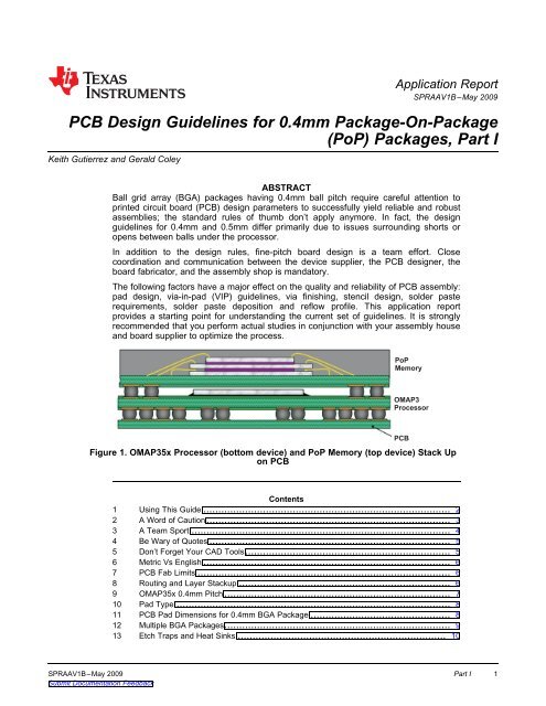
PoP<br />
Memory<br />
OMAP3<br />
Processor<br />
<strong>PCB</strong><br />
Figure 1. OMAP35x Processor (bottom device) and PoP Memory (top device) Stack Up<br />
on <strong>PCB</strong><br />
Contents<br />
1 Using This Guide ................................................................................... 2<br />
2 A Word of Caution.................................................................................. 3<br />
3 A Team Sport ....................................................................................... 4<br />
4 Be Wary of Quotes ................................................................................. 5<br />
5 Don’t Forget Your CAD Tools..................................................................... 5<br />
6 Metric Vs English ................................................................................... 6<br />
7 <strong>PCB</strong> Fab Limits ..................................................................................... 6<br />
8 Routing and Layer Stackup ....................................................................... 6<br />
9 OMAP35x <strong>0.4mm</strong> Pitch............................................................................ 7<br />
10 Pad Type ............................................................................................ 8<br />
11 <strong>PCB</strong> Pad Dimensions <strong>for</strong> <strong>0.4mm</strong> BGA <strong>Package</strong> ............................................... 8<br />
12 Multiple BGA <strong>Package</strong>s............................................................................ 9<br />
13 Etch Traps and Heat Sinks ...................................................................... 10<br />
SPRAAV1B–May 2009 Part I 1<br />
Submit Documentation Feedback
Using This Guide www.ti.com<br />
1 Using This Guide<br />
14 Vias and VIP....................................................................................... 11<br />
15 Laser Blind Vias ................................................................................... 12<br />
16 Filled Vias .......................................................................................... 12<br />
17 Know Your Tools.................................................................................. 13<br />
18 BeagleBoard ....................................................................................... 13<br />
19 BeagleBoard Views ............................................................................... 14<br />
20 OMAP35x Decoupling ............................................................................ 21<br />
21 <strong>PCB</strong> Finishes <strong>for</strong> HDI............................................................................. 22<br />
22 Real World Second Opinion ..................................................................... 23<br />
23 Acknowledgments................................................................................. 24<br />
24 References......................................................................................... 24<br />
List of Figures<br />
1 OMAP35x Processor (bottom device) and PoP Memory (top device) Stack Up on <strong>PCB</strong>. 1<br />
2 Part 1 - Focus <strong>for</strong> Part I - <strong>PCB</strong> <strong>Design</strong> <strong>Guidelines</strong>............................................. 3<br />
3 Focus <strong>for</strong> Part II - Assembly <strong>Guidelines</strong>......................................................... 3<br />
4 PoP Assembly Teamwork ......................................................................... 5<br />
5 OMAP35x - CBB <strong>Package</strong> Specification Details ............................................... 7<br />
6 OMAP35x - CBB <strong>Package</strong> ........................................................................ 7<br />
7 Solder-Mask-Defined (SMD) and Non-Solder-Mask-Defined (NSMD) Pads ............... 8<br />
8 Recommendations <strong>for</strong> <strong>0.4mm</strong> Pitch <strong>Package</strong>s - Top Layer .................................. 9<br />
9 Multiple BGA Pacbages on <strong>PCB</strong> Should Be Off-Set........................................... 9<br />
10 Multiple BGA <strong>Package</strong>s on <strong>PCB</strong> Should not Be Overlapped ............................... 10<br />
11 Common Sense Routing Circuit Board <strong>Guidelines</strong> ........................................... 10<br />
12 Common Sense Routing Circuit Board <strong>Guidelines</strong> ........................................... 11<br />
13 BeagleBoard Via Example....................................................................... 11<br />
14 Plated, Filled and Capped BGA Pad ........................................................... 12<br />
15 Effect af an Uncapped Via ....................................................................... 12<br />
16 BeagleBoard.org .................................................................................. 13<br />
17 Top Layer BeagleBoard Layout ................................................................. 14<br />
18 BeagleBoard Top Layer Underneath the OMAP35x ......................................... 15<br />
19 Close-Up of BeagleBoard Layer 1 - Top Side................................................. 16<br />
20 Close-Up of BeagleBoard Layer 2 - Ground Plane........................................... 17<br />
21 Close-Up of BeagleBoard Layer 3 - Internal Signal .......................................... 18<br />
22 Close-Up of BeagleBoard Layer 4 - Internal Signal .......................................... 19<br />
23 Close-Up of BeagleBoard Layer 5 - Power Plane ............................................ 20<br />
24 Close-Up of BeagleBoard Layer 6 - Bottom Side............................................. 21<br />
25 BeagleBoard Bypass Group <strong>for</strong> V DD2........................................................... 22<br />
26 First Pass DFM of the OMAP35x EVM......................................................... 23<br />
List of Tables<br />
1 2003 SMTA Paper Summary of Attributes of Each <strong>PCB</strong> Finish ............................ 23<br />
This application report focuses on circuit board design guidelines specific to the OMAP35x processor, with<br />
<strong>0.4mm</strong> pitch on the bottom and 0.5mm pitch pads on the top <strong>for</strong> memory attachment, using<br />
package-on-package technology. Experience has shown that <strong>PCB</strong> board design is the most crucial aspect<br />
of PoP design due to the extremely small pad pitches. Also, not all assembly houses can build such small<br />
pitch assemblies or properly mount the memory on top of the processor.<br />
MicroStar BGA is a trademark of <strong>Texas</strong> <strong>Instruments</strong>.<br />
All other trademarks are the property of their respective owners.<br />
2 Part I SPRAAV1B–May 2009<br />
Submit Documentation Feedback
www.ti.com A Word of Caution<br />
Figure 2 shows a <strong>0.4mm</strong> pitch processor and its matching memory at 0.5mm pitch.<br />
2 A Word of Caution<br />
Figure 2. Part 1 - Focus <strong>for</strong> Part I - <strong>PCB</strong> <strong>Design</strong> <strong>Guidelines</strong><br />
<strong>Guidelines</strong> <strong>for</strong> the assembly of <strong>PCB</strong>s that use the PoP package are covered in the companion article to<br />
this document, <strong>PCB</strong> Assembly <strong>Guidelines</strong> <strong>for</strong> <strong>0.4mm</strong> <strong>Package</strong>-<strong>On</strong>-<strong>Package</strong> (PoP) <strong>Package</strong>s, Part II<br />
(SPRAAV2) - which will be referred to as Part II throughout the remainder of this document. Included are<br />
assembly options and suggestions to use when qualifying and working with your assembly sites, either<br />
internal or contract.<br />
Figure 3. Focus <strong>for</strong> Part II - Assembly <strong>Guidelines</strong><br />
This section discusses the BGA package and the circuit board immediately below the BGA. The<br />
guidelines do not cover all aspects of circuit board design, nor is it a discussion on how to use your<br />
favorite CAD tool.<br />
SPRAAV1B–May 2009 Part I 3<br />
Submit Documentation Feedback
A Team Sport www.ti.com<br />
<strong>Design</strong> of circuit boards <strong>for</strong> fine-pitch BGA packages at <strong>0.4mm</strong> and smaller is more of an art than a<br />
science, due to the lack of published data. In many cases, <strong>0.4mm</strong> pitch pcb fabrication technology is<br />
considered proprietary and/or advanced and may require that a non-disclosure-agreement (NDA) be<br />
executed. There<strong>for</strong>e, the material in this document will age and go out of date quickly as more assembly<br />
houses adopt smaller pitches and PoP assembly.<br />
Since this is a rapidly evolving technology, spend some time reading the huge number of articles, papers<br />
and company presentations on all aspects of fine-pitch board design.<br />
When the 0.5mm pitch design guidelines were created, it was stated that the long standing rules <strong>for</strong> circuit<br />
board design were no longer applicable at these small geometries and a new batch of guidelines were<br />
established. With the release of <strong>0.4mm</strong> pitch BGA packages, the new rules needed to be modified. This<br />
was determined through the design and assembly of TI developed evaluation module (EVM) boards and a<br />
new circuit design called the BeagleBoard.<br />
The BeagleBoard is referenced extensively throughout this document and Part II. Be sure to obtain the<br />
Gerber files <strong>for</strong> this board at http://beagleboard.org. The files will be an invaluable reference during the<br />
design of your board. Also be sure to check <strong>for</strong> updates to this document which will be found on the<br />
beagleboard.org website as well as all TI websites <strong>for</strong> OMAP35x, Application Notes Section.<br />
It is strongly recommended that you plan on per<strong>for</strong>ming your own experimental layouts and prototype runs<br />
be<strong>for</strong>e committing to volume production to determine if: your suppliers can handle the device, you may<br />
have to change circuit board vendors, and/or find assembly shops with better equipment.<br />
<strong>On</strong>e important aspect of <strong>0.4mm</strong> design is the need <strong>for</strong> close cooperation among the various entities that<br />
are involved in the board design, fabrication, and assembly.<br />
3 A Team Sport<br />
Successful design and assembly of complex, fine-pitch circuit boards is a Team Sport. The days of tossing<br />
circuit diagrams over the cubical wall to the board designer who then tosses them to the assembly shop<br />
are gone. Today’s board design requires a team approach and the entire process, from component<br />
selection to assembly requires careful coordination.<br />
The typical team is composed of four different members representing the four major steps in product<br />
fabrication: the device supplier (chips, passives, mechanical), the <strong>PCB</strong> designer, the <strong>PCB</strong> fabrication<br />
shop, and the <strong>PCB</strong> assembly shop. There may be more members or some members may do more than<br />
one job.<br />
Each of the team members brings their own experiences and design guidelines to bear on the task. As a<br />
result, it is not uncommon to find conflicting guidelines. These conflicts must be resolved prior to the start<br />
of work. Unresolved conflicts will result in poor assembly yields at best or 100% failure at worst. Constant<br />
and frequent communication is the key to resolving conflicts and everyone must be in the loop.<br />
Get to know your team members and be sure to have frequent meetings as the project proceeds from<br />
design through production. It will be money and time well spent.<br />
Part I<br />
4 SPRAAV1B–May 2009<br />
Submit Documentation Feedback
www.ti.com Be Wary of Quotes<br />
4 Be Wary of Quotes<br />
5 Don’t Forget Your CAD Tools<br />
Figure 4. PoP Assembly Teamwork<br />
Board fabrication cost estimates vary widely. There are two key parameters that go into the overall quote<br />
cost: 1) Experience with fine pitch fabrication and 2) The quantity of boards in the production run.<br />
Several board design and layout options are described with some options featuring a lower price.<br />
However, the lower price assumes that a relatively large number of boards are being fabricated. For<br />
smaller volumes, or <strong>for</strong> prototyping, the cost may be the same or even higher <strong>for</strong> some options.<br />
Also, be wary of quick quotes that seem out of line. In many cases, the board vendor may be using<br />
outdated design rules causing a relatively high dollar quote <strong>for</strong> what might now be standard technology.<br />
Press them hard <strong>for</strong> ways to lower the cost. And be sure to obtain several quotes or get a second opinion.<br />
Review the microvia capabilities of your CAD system. Blind microvias open up routing channels on the<br />
inner layers. There<strong>for</strong>e, your CAD system must be capable of handling blind and buried microvias as well<br />
as through-hole vias. Your system’s features and setup dictates the difficulty or ease with which the board<br />
will route. Some of the setup parameters include via size, span, and a whole slew of clearance rules. Most<br />
CAD vendors offer specialized training on high-density interconnects and fine-pitch BGA circuit boards.<br />
Talk to them – they are part of your design team, too.<br />
Your CAD tools can also help with the DFM checking task; take advantage of those tools. Each CAD<br />
plat<strong>for</strong>m is different and has different capabilities. For example, the Altium <strong>PCB</strong> design rules checking<br />
section spans more than 119 pages. Your particular CAD plat<strong>for</strong>m will have various checks and tests that<br />
can be per<strong>for</strong>med on the finished circuit board design. Learn them and use them.<br />
SPRAAV1B–May 2009 Part I 5<br />
Submit Documentation Feedback
Metric Vs English www.ti.com<br />
6 Metric Vs English<br />
Here is one of the most common complaints about moving to fine-pitch BGA package design – use of the<br />
metric system. Most designers dislike this simply because all of their familiar rule-of-thumb guidelines are<br />
in the English system. Quick test, which is easier to understand 0.0033” or 83 μm? It is strongly suggested<br />
to set up your CAD grid in micrometers (μm) and do away with the four decimal places of accuracy<br />
needed to represent small features in the English system.<br />
7 <strong>PCB</strong> Fab Limits<br />
Most circuit board vendors publish a table that indicates various limits <strong>for</strong> drills, trace widths, thicknesses<br />
and so on. In many cases, there are different limits depending on the most important characteristic <strong>for</strong> the<br />
board. What this means is that there are tradeoffs and options <strong>for</strong> the designer to consider. Always consult<br />
with your circuit board vendor <strong>for</strong> their limits and capabilities and remember that as you approach the limit<br />
of the vendor’s equipment, yields go way down and costs go way up. Let’s look at one vendor's (vendor X)<br />
technology and capabilities:<br />
Standard Technology—Usually means this is the middle of the vendor’s capability and pricing. The<br />
technology does not push the limits of the vendor’s equipment. For example, vendor X shows that a<br />
standard minimum trace width and clearance are 3 mils with 4 mil vias and 10 mil pads.<br />
High Yield Technology—Loosens up the specifications to provide more clearance and wider traces<br />
resulting in lower cost per unit board and higher yields. For example, the same vendor X lists a<br />
minimum trace width and minimum clearance of 4 mils with 4 mil vias and 10 mil pads <strong>for</strong> high yield<br />
boards. However, a hi-yield board may be larger and have more layers.<br />
Engineering Development Technology— Really pushes the vendor’s capabilities. It is at the limits of the<br />
vendor’s equipment. For example, vendor X lists a minimum trace width and minimum clearance of<br />
2.5 mils with 3 mil vias and 9 mil pads.<br />
8 Routing and Layer Stackup<br />
<strong>On</strong>e huge benefit of PoP is the elimination of the high-speed, balanced transmission lines between the<br />
processor and memory. The external memory’s data and control lines no longer have to be routed out<br />
from under the processor. This is a huge savings in both time and the number of layers. This also impacts<br />
your pad and layer stackup decisions. OEMs have quickly adopted PoP as their processor/memory<br />
package of choice <strong>for</strong> these reasons.<br />
It is possible to use a 6-layer stack and route all of the connections without requiring buried vias. For the<br />
BeagleBoard, relatively common VIP technology was used. There are several suitable layer setups; the<br />
one described below was used in the BeagleBoard. This <strong>for</strong>mat is also popular because it allows sensitive<br />
clock signals or relatively high-speed lines to be routed between power planes.<br />
Layer 1 Signal (Top Copper)<br />
Layer 2 Ground<br />
Layer 3 Signal<br />
Layer 4 Signal<br />
Layer 5 Power<br />
Layer 6 Signal (Bottom Copper)<br />
<strong>Package</strong> footprints and pad stacks are the next important item to consider. Proper definitions and strict<br />
adherence to clearance plays a key role in the development of high yield PoP designs.<br />
Part I<br />
6 SPRAAV1B–May 2009<br />
Submit Documentation Feedback
www.ti.com OMAP35x <strong>0.4mm</strong> Pitch<br />
9 OMAP35x <strong>0.4mm</strong> Pitch<br />
Familiarity with the basic dimensions of the OMAP35x processor is helpful. This section discusses the key<br />
parameters.<br />
Figure 5. OMAP35x - CBB <strong>Package</strong> Specification Details<br />
Figure 6. OMAP35x - CBB <strong>Package</strong><br />
SPRAAV1B–May 2009 Part I 7<br />
Submit Documentation Feedback
Pad Type www.ti.com<br />
10 Pad Type<br />
It is important to understand the pros, cons, and unknowns concerning the two most common types of<br />
solder pads. Figure 7 shows the solder-mask-defined (SMD) and non-solder-mask-defined (NSMD) pads.<br />
Figure 7. Solder-Mask-Defined (SMD) and Non-Solder-Mask-Defined (NSMD) Pads<br />
Industry reliability studies have revealed that NSMD-type pads are highly recommended <strong>for</strong> most 0.5mm<br />
pitch BGA applications. However, there is a problem with this approach at <strong>0.4mm</strong> pitch.<br />
Real-world assembly experiments with the BeagleBoard and the OMAP35x EVM revealed a tendency <strong>for</strong><br />
solder bridging between pads when NSMD were used. There was insufficient solder mask webbing<br />
between the pads to ward off bridging. There<strong>for</strong>e, a SMD design was used which resulted in much better<br />
assembly yields with no solder bridging.<br />
Talk to your board fabricator and your board assembly house and learn of their experiences and<br />
preferences be<strong>for</strong>e deciding which type of pad design you will use. Be prepared to change your ideas<br />
about pad definitions as your experience grows with <strong>0.4mm</strong> pitch parts.<br />
Note: Based on experience with both the BeagleBoard and the OMAP35x EVM, the use of<br />
solder-mask-defined pads is recommended.<br />
11 <strong>PCB</strong> Pad Dimensions <strong>for</strong> <strong>0.4mm</strong> BGA <strong>Package</strong><br />
Through several meetings with both board fabricators and board assembly houses, the following<br />
recommendation has been created <strong>for</strong> the circuit board BGA footprint <strong>for</strong> the OMAP35x having <strong>0.4mm</strong> or<br />
400 μm, pitch solder balls. Figure 8 shows the top layer with vias down to layer 2.<br />
At the <strong>0.4mm</strong> pitch, there is insufficient space between pads to allow a 3mil trace to run between pads<br />
without incurring solder bridging. There<strong>for</strong>e, except <strong>for</strong> the outside perimeter balls, all connections are<br />
routed to the lower layers through VIP technology. With this technology, only six layers were needed <strong>for</strong><br />
the BeagleBoard.<br />
For the BeagleBoard design, the desired finished pad size is equal to the solder ball diameter. Since no<br />
traces run between the pads, the copper pad is enlarged to 280 μm (11mils). The solder mask opening is<br />
set to 254 μm (10 mils).<br />
With this arrangement, there is plenty of solder webbing between pads which helps prevent adjacent ball<br />
solder bridging. For more in<strong>for</strong>mation regarding additional parameters that impact the assembly of this<br />
package, see <strong>PCB</strong> Assembly <strong>Guidelines</strong> <strong>for</strong> <strong>0.4mm</strong> <strong>Package</strong>-<strong>On</strong>-<strong>Package</strong> (PoP) <strong>Package</strong>s, Part II<br />
(SPRAAV2).<br />
Part I<br />
8 SPRAAV1B–May 2009<br />
Submit Documentation Feedback
www.ti.com Multiple BGA <strong>Package</strong>s<br />
Pad Type Solder Mask Defined<br />
Pad Pitch A 400 μm (<strong>0.4mm</strong>)<br />
Mask Opening B 254 μm (10mils)<br />
Pad Size C 280 μm (11mils)<br />
Mask Shape Round<br />
Mask Web D 150 μm<br />
Pad to Pad Clearance E 120 μm<br />
Trace Allowed Between No<br />
12 Multiple BGA <strong>Package</strong>s<br />
Figure 8. Recommendations <strong>for</strong> <strong>0.4mm</strong> Pitch <strong>Package</strong>s - Top Layer<br />
When BGA packages are placed on the top and bottom layers, do not place one BGA package directly<br />
underneath another BGA package. The temperature cycle board level reliability degrades if overlap of<br />
package footprint occurs.<br />
Figure 9. Multiple BGA Pacbages on <strong>PCB</strong> Should Be Off-Set<br />
Several studies, including the one referenced here, show that temperature cycle board-level-reliability<br />
(BLR) per<strong>for</strong>mance degrades if there is an overlap of package footprints. A small BGA opposite a large<br />
BGA or QFP, with its footprint within the unpopulated I/O shadow of the larger package, has temperature<br />
cycle per<strong>for</strong>mance similar to that of a single-side board assembly.<br />
SPRAAV1B–May 2009 Part I 9<br />
Submit Documentation Feedback
Etch Traps and Heat Sinks www.ti.com<br />
13 Etch Traps and Heat Sinks<br />
Figure 10. Multiple BGA <strong>Package</strong>s on <strong>PCB</strong> Should not Be Overlapped<br />
For additional in<strong>for</strong>mation on this concept, please see section 5.4, Single-Sided Soldering and<br />
Double-Sided Soldering, of NEC’s, Semicondutor Device Mount Manual,<br />
http://www.necel.com/pkg/en/mount/.<br />
The challenge with fine pitch board design is to insure that traces and vias don’t pull heat away from the<br />
solder ball pad. This means that common sense routing circuit board guidelines are still useable. Also<br />
beware of etch traps.<br />
Figure 11. Common Sense Routing Circuit Board <strong>Guidelines</strong><br />
Small BGA pads don’t have much solder and depend on uni<strong>for</strong>m heating <strong>for</strong> a good joint. Here are some<br />
additional tips to insure that traces and vias don’t serve as heatsinks.<br />
• Keep the trace smaller than the pad or via.<br />
• Do not gang up pads with a copper pour such as around a ground plane.<br />
• Use individual traces to interconnect the pads.<br />
The OMAP35x processors are relatively low power devices so the smaller traces are appropriate.<br />
Part I<br />
10 SPRAAV1B–May 2009<br />
Submit Documentation Feedback
www.ti.com Vias and VIP<br />
14 Vias and VIP<br />
Figure 12. Common Sense Routing Circuit Board <strong>Guidelines</strong><br />
<strong>On</strong>e of the greatest benefits from package-on-package technology is the elimination of the complex,<br />
expensive, and challenging task of routing high-speed memory lines from under the processor out to<br />
memory. Instead, the memory sits on top of the processor and the connections are automatically made<br />
during assembly.<br />
Except <strong>for</strong> the outer perimeter balls, routing <strong>for</strong> the BeagleBoard is done with VIP technology. Although<br />
this was once a feared and expensive technology, recent studies and advances have eliminated nearly all<br />
of the problems. In fact, VIP is becoming the dominate technology <strong>for</strong> high density boards and is providing<br />
a cost effective alternative to conventional and offset vias.<br />
The VIP methodology places the via directly under the device’s balls. However, this requires another step<br />
to seal the via to prevent blowouts and voids. For the BeagleBoard, non-conductive, epoxy-filled vias were<br />
used.<br />
The BeagleBoard uses only through-hole vias from top to bottom, blind vias from top to layer 2, and<br />
stacked vias from top layer to layer 3. It does not use buried vias. All vias are laser drilled.<br />
Figure 13. BeagleBoard Via Example<br />
SPRAAV1B–May 2009 Part I 11<br />
Submit Documentation Feedback
Laser Blind Vias www.ti.com<br />
15 Laser Blind Vias<br />
The BeagleBoard uses blind vias that are 6mil in diameter and are laser drilled.<br />
Laser vias are typically drilled through rein<strong>for</strong>ced FR-4 material that is 0.002” thick or less. There is<br />
standard FR-4 or laser drillable FR-4 that uses a more uni<strong>for</strong>m glass weave. The LD glass has a cost<br />
adder to it, but produces a smoother wall hole surface which makes filling and capping easier.<br />
The minimum average copper plating thickness <strong>for</strong> a laser blind via hole should be specified as 0.0005” or<br />
as In accordance with IPC-6012A, class 2.<br />
16 Filled Vias<br />
After drilling, and depending on the board fabricator preferences, the BeagleBoard vias were filled with<br />
non-conductive epoxy. It was used because it has a better match to the thermal expansion properties of<br />
the board material.<br />
<strong>On</strong>ce the vias are filled, cured, and planarized, they are then plated. This yields a flat copper plated cap<br />
over the vias which facilitates component attachment. The VIP technology provides two primary benefits:<br />
higher component density and improved routing.<br />
Figure 14. Plated, Filled and Capped BGA Pad<br />
All vias must be capped or filled to prevent voids and out gassing. The images inFigure 15 show the effect<br />
of an uncapped via. The voids and damage occurs during reflow. The right picture is a failure caused by<br />
the excessive package movement during reflow, caused by out gassing.<br />
Solder Ball<br />
Unfilled Pad with Via<br />
Void Caused by<br />
Trapped Air<br />
Figure 15. Effect af an Uncapped Via<br />
It is strongly recommended that all vias be tented, filled and/or capped, especially under BGA packages.<br />
Be sure to consult with your board fabricator prior to specifying via fill to establish their manufacturing<br />
requirements. Also, make sure your CAD system provides the required design files and the needed<br />
documentation. In some cases, additional files may be required.<br />
Tom Hausherr, from PCLibraries (www.pcblibraries.com), has a very good presentation covering various<br />
types of vias and via coverings. His presentation, Metric Pitch BGA and Micro BGA Routing Solutions, can<br />
be found on their website. Please read that material since this application report only highlights the three<br />
most commonly used types of vias and via coverings.<br />
Part I<br />
12 SPRAAV1B–May 2009<br />
Submit Documentation Feedback
www.ti.com Know Your Tools<br />
17 Know Your Tools<br />
Beware that your CAD program must be setup correctly to define the appropriate pad and via stacks to<br />
support different types of vias. The additional process steps may require additional gerber files.<br />
Your CAD manual and board fabricator will be your best friends as your tools are setup, so plan to learn<br />
and use all available supporting documentation as well as your extended team members.<br />
Here are some precautions and checks you might consider after your board has been sent through the<br />
autorouter:<br />
• Too many vias – Power routing without constraints can result in some traces becoming overly long with<br />
too many vias. This can adversely impact the impedance of the subsequent trace, resulting in<br />
excessive noise pickup.<br />
• Insufficient trace width – Be sure that power traces have adequate width. In the BeagleBoard example,<br />
notice the use of wide traces <strong>for</strong> all power nets, especially on the inner layers. Inner layer power traces<br />
are 10 mils on the BeagleBoard.<br />
• Use the power planes <strong>for</strong> routing – Although not always mentioned, the power planes can be used <strong>for</strong><br />
routing. This can be seen on the ground layer of the BeagleBoard.<br />
• Add additional planes on other layers – The BeagleBoard has low routing density on several planes<br />
allowing <strong>for</strong> copper pours <strong>for</strong> other power planes on these layers.<br />
• Use multiple power planes on the power plane. Three different power rails are routed on the power<br />
plane layer and each one is an individual copper pour. Each power rail has its own set of bypass<br />
capacitors even though they share the same layer.<br />
Note: It is strongly recommended that all vias be covered, especially under BGA packages. In<br />
addition, the board vendor should be consulted prior to specifying via fill to establish their<br />
manufacturing requirements, required design files, and the needed documentation.<br />
18 BeagleBoard<br />
The BeagleBoard is an open-source hardware plat<strong>for</strong>m based on the <strong>Texas</strong> <strong>Instruments</strong>' OMAP35x. The<br />
plat<strong>for</strong>m is a complete single board computer suitable <strong>for</strong> software development and debug. Use the<br />
following link <strong>for</strong> additional in<strong>for</strong>mation, including the hardware schematics and Gerber files:<br />
http://beagleboard.org. Also consider subscribing to the BeagleBoard RSS feed.<br />
Figure 16. BeagleBoard.org<br />
The BeagleBoard is used to illustrate the use of the <strong>0.4mm</strong> <strong>PCB</strong> design guidelines and the assembly<br />
guidelines discussed in <strong>PCB</strong> Assembly <strong>Guidelines</strong> <strong>for</strong> <strong>0.4mm</strong> <strong>Package</strong>-<strong>On</strong>-<strong>Package</strong> (PoP) <strong>Package</strong>s, Part<br />
II (SPRAAV2). Figure 17 shows the board layout. Subsequent sections discuss each layer as it is used to<br />
route the BeagleBoard with special attention given to the area under the OMAP35x device. The overall<br />
board dimensions are 3 inches by 3.1 inches and it is a 6 layer board.<br />
Copies of the Gerber files and schematics from the BeagleBoard website provide an example of a real<br />
layout that has gone to production.<br />
SPRAAV1B–May 2009 Part I 13<br />
Submit Documentation Feedback
BeagleBoard Views www.ti.com<br />
19 BeagleBoard Views<br />
Figure 17. Top Layer BeagleBoard Layout<br />
Each BeagleBoard layer is shown, with the image centered on the area underneath the OMAP35x.<br />
The layer images are from the Allegro viewer with the appropriate pins, vias, and etch turned on <strong>for</strong> each<br />
layer. Except <strong>for</strong> the overall board picture shown in Figure 17, the area underneath the BGA package is<br />
the focal point. The image is always shown from the top.<br />
The color code used is green <strong>for</strong> etch, blue <strong>for</strong> vias, gray <strong>for</strong> component pads, and blue-gray <strong>for</strong> the VIP.<br />
The solid dark square is the OMAP35x outline and is retained <strong>for</strong> each subsequent layer.<br />
Part I<br />
14 SPRAAV1B–May 2009<br />
Submit Documentation Feedback
www.ti.com BeagleBoard Views<br />
Figure 18 is the top layer with the various pads and trace widths annotated.<br />
Figure 18. BeagleBoard Top Layer Underneath the OMAP35x<br />
SPRAAV1B–May 2009 Part I 15<br />
Submit Documentation Feedback
BeagleBoard Views www.ti.com<br />
19.1 Top Layer – Signal - Area Underneath the OMAP35x<br />
Things to notice on this layer:<br />
• No traces between BGA pads<br />
• The thin traces are all 3mil width<br />
• Thick traces are 10mils<br />
• The VIP are blind and go from 1-2 or 1-3 only. There are no buried vias.<br />
Figure 19. Close-Up of BeagleBoard Layer 1 - Top Side<br />
16 Part I SPRAAV1B–May 2009<br />
Submit Documentation Feedback
www.ti.com BeagleBoard Views<br />
19.2 Layer 2 – Ground<br />
The ground plane is the shaded green area.<br />
VIO_1V8<br />
VDD2<br />
VDD2<br />
Figure 20. Close-Up of BeagleBoard Layer 2 - Ground Plane<br />
SPRAAV1B–May 2009 Part I 17<br />
Submit Documentation Feedback
BeagleBoard Views www.ti.com<br />
19.3 Layer 3 – Signal<br />
Figure 21. Close-Up of BeagleBoard Layer 3 - Internal Signal<br />
18 Part I SPRAAV1B–May 2009<br />
Submit Documentation Feedback
www.ti.com BeagleBoard Views<br />
19.4 Layer 4 – Signal<br />
Figure 22. Close-Up of BeagleBoard Layer 4 - Internal Signal<br />
SPRAAV1B–May 2009 Part I 19<br />
Submit Documentation Feedback
BeagleBoard Views www.ti.com<br />
19.5 Layer 5 – Power (V DD2)<br />
VCORE_1V3<br />
10 mil Width<br />
VDD2<br />
VIO_1V8<br />
VIO_1V8<br />
Figure 23. Close-Up of BeagleBoard Layer 5 - Power Plane<br />
19.6 Layer 6 – Signal – Bottom Copper – Bottom Component Outlines<br />
The bottom layer view has been enlarged in scope to show more of the board and to show most of the<br />
OMA35xx supply bypass capacitors (shown in orange.) The two small black colored items are resistors.<br />
The X7R bypass capacitors are the smaller 0402 packages and are all rated at 0.1μF/10 V. The three<br />
larger capacitors are all 1μF and are used to bypass the OMAP3 processor’s internally derived voltages<br />
and references.<br />
Part I<br />
20 SPRAAV1B–May 2009<br />
Submit Documentation Feedback
www.ti.com OMAP35x Decoupling<br />
20 OMAP35x Decoupling<br />
Figure 24. Close-Up of BeagleBoard Layer 6 - Bottom Side<br />
There are a lot of power pins on the OMAP35x. Decoupling capacitors are required and must be placed<br />
as close to the ball connection as possible. When selecting a power and ground, choose the ground<br />
closest to the power pin <strong>for</strong> each decoupling capacitor. A single decoupling capacitor can serve up to<br />
three balls.<br />
The BeagleBoard has almost all of its decoupling capacitors mounted on the bottom side of the board.<br />
Each capacitor connects with as many as three processor power pins through both blind vias to the power<br />
plane and thru-hole vias from top to bottom.<br />
Figure 25 shows how the OMAP335xx’s V DD2 rail is decoupled on the BeagleBoard. The processor outline<br />
is shown as a dotted line and the <strong>PCB</strong> design is viewed from the top side. The schematic <strong>for</strong> this area is<br />
shown to the right and the reference designators are shown on the appropriate capacitors.<br />
The bypass capacitors are 0.1μF, 10 V, X7R type and are in a 0402 package.<br />
There are additional voltage rails that use the remaining capacitors. A careful study of the BeagleBoard<br />
Gerbers and schematics will help you as your design is realized and illustrate what worked <strong>for</strong> this board.<br />
SPRAAV1B–May 2009 Part I 21<br />
Submit Documentation Feedback
<strong>PCB</strong> Finishes <strong>for</strong> HDI www.ti.com<br />
21 <strong>PCB</strong> Finishes <strong>for</strong> HDI<br />
Figure 25. BeagleBoard Bypass Group <strong>for</strong> V DD2<br />
A surface finish provides a coating over the outer layer copper that prevents oxidation and provides an<br />
electrically conductive surface. This surface has two generic functional requirements: to provide a<br />
solderable surface <strong>for</strong> connecting components with solder and to attach a component without soldering,<br />
such as a wire bond or press-fit connector.<br />
Organic Solderability Preservative (OSP)—This process coats a very thin coating of an organic material<br />
that inhibits copper oxidation. It is so thin that it is nearly impossible to see and measure. The<br />
organic material is removed by the assembly flux. Boards that have been OSP coated will have<br />
bright copper pad coloration. The most prevalent is ENTEK CU-106A. This is used <strong>for</strong> assemblies<br />
that will go through multiple assembly operations. <strong>PCB</strong>’s that have multiple surface finishes can use<br />
the CU-106A(X) finish.<br />
Immersion Tin (ImSn)—This process coats a thin layer of tin directly on top of the copper surface. The<br />
tin produces an extremely flat surface <strong>for</strong> mounting of surface mount components with ultra<br />
fine-pitch devices. This also provides a thicker, uni<strong>for</strong>m surface that provides lubrication <strong>for</strong> press-fit<br />
pins.<br />
Immersion Silver (ImAg)—This process plates a thin layer of silver directly on top of the copper surface.<br />
As with the other immersion surface finishes, the finished product produces a very flat surface; it is<br />
ideal <strong>for</strong> fine pitch SMD arrays. This surface finish has the ability to maintain high solderability after<br />
multiple heat cycles. This can also be used as an aluminum wire bondable surface. It is compatible<br />
with no-clean assembly processes. This is becoming popular as a HASL replacement <strong>for</strong> lead-free<br />
soldering applications. This surface finish yields a dull tarnished looking surface. There is significant<br />
industry data showing that the dullness does not affect solderability or reliability.<br />
Part I<br />
22 SPRAAV1B–May 2009<br />
Submit Documentation Feedback
www.ti.com Real World Second Opinion<br />
Other Finishes—Other finishes include hot-air solder leveling and immersion nickel-gold (ImNiAu).<br />
Table 1, from a 2003 SMTA paper, summarizes the attributes of each <strong>PCB</strong> finish.<br />
22 Real World Second Opinion<br />
Table 1. 2003 SMTA Paper Summary of Attributes of Each <strong>PCB</strong> Finish<br />
Parameter HASL OSP ENIG ImAg ImSn<br />
Standard solder joints are P P P P P<br />
predictable<br />
BGA solder joints are P P M P P<br />
predictable<br />
Solderability shelf life is one P M P M M<br />
year<br />
Soldermask compatibility P P M P M<br />
Via plugging is safe and P M P M M<br />
reliable<br />
Improves overall via reliability M --–- P --–- --–-<br />
Flat surface benefits assembly M P P P P<br />
Conductive contact surface P M P P P<br />
Solderable over four heating P P M P P<br />
cycles<br />
Thickness variation is minimal M P P P P<br />
Coating is environment friendly M P P P P<br />
Tin whiskers are not a problem P P P P M<br />
P = plus, M = minus, N = 8P 8P 9P 9P 7P<br />
neutral<br />
Our first OMAP35x EVM circuit board was designed prior to the release of these guidelines and was<br />
submitted to an assembly house. Elcotech, where they per<strong>for</strong>med a DFM analysis on the gerber files.<br />
Below are their comments and Figure 26 shows this first pass at the EVM layout.<br />
Figure 26. First Pass DFM of the OMAP35x EVM<br />
SPRAAV1B–May 2009 Part I 23<br />
Submit Documentation Feedback
Acknowledgments www.ti.com<br />
This demonstrates how important good communication is between all members of the design team. Had<br />
this board gone into production, the yield would have been very poor. Our thanks to Elcoteq in<br />
Richardson, TX <strong>for</strong> their analysis from which this section was created. The list below has their comments<br />
tied to the various locations annotated in Figure 26.<br />
• At location A, seven BGA Pads are ganged together. This acts as a large heatsink during reflow.<br />
• The traces between D and the BGA pad should be narrower. A trace entering a pad should never be<br />
larger than the diameter of the pad.<br />
• In some cases the BGA to ground plane is done like D and other it is done like A. Neither are good<br />
techniques.<br />
• In C, the trace width exiting the BGA pad is much too large. In this case the trace acts as a heatsink<br />
during reflow.<br />
• As in details A,B,C and D, the heat transfer from the ground planes is passing through a large via<br />
through a large trace and fanned out across 7 BGA pads ganged together.<br />
• Do not gang BGA pads together with a copper plane as this increases the heat sink effect.<br />
23 Acknowledgments<br />
• Clint Cooley and Franklin Troung, CircuitCo, 675 N. Glenville #195, Richardson, TX 75081,<br />
214-466-6690, www.CircuitCo.com<br />
• Elcoteq, Sinimaentie 8B, P.O. Box 8, FI-02631 Espoo, Finland<br />
• Micron Technology, Inc., 8000 South Federal Way, Post Office Box 6, Boise, ID 83707-0006<br />
24 References<br />
• Printed Circuits Handbook - 6th Edition, Clyde Coombs, Jr., McGraw-Hill, January 2008<br />
• <strong>PCB</strong> <strong>Design</strong> and SMT Assembly/Rework <strong>Guidelines</strong> <strong>for</strong> MCM-L <strong>Package</strong>s, 2001–2006, Skyworks<br />
Solutions, Inc. All Rights Reserved.<br />
• Semicondutor Device Mount Manual, http://www.necel.com/pkg/en/mount/<br />
• <strong>PCB</strong> Assembly <strong>Guidelines</strong> <strong>for</strong> <strong>0.4mm</strong> <strong>Package</strong>-<strong>On</strong>-<strong>Package</strong> (PoP) <strong>Package</strong>s, Part II (SPRAAV2)<br />
• PC-Board Layout Techniques <strong>for</strong> ML67Q4060/4061 ARM 7 W-CSP <strong>Package</strong>d Devices, October 5,<br />
2005, Rev 1.0, OKI Semiconductor<br />
• <strong>PCB</strong> Pad Pattern <strong>Design</strong> and Surface-Mount Considerations, XAPP439 (v1.0), April 11, 2005, Xilinix<br />
• Eliminating Microvoid Risk Via An Optimized Surface Finish Process, Donald Cullen, Witold Paw, John<br />
Swanson, Lenora Toscano, MacDermid, Inc. Waterbury, CT USA<br />
• Effect Of Printed Wiring Board Warpage <strong>On</strong> Ball Grid Arrays Over Temperature, Kyra Ewer and Jeffrey<br />
Seekatz Raytheon, Dallas, TX. 2004<br />
• <strong>Design</strong> Method <strong>for</strong> High Reliable Flip Chip BGA <strong>Package</strong>, Naoto Saito, Hitachi Ltd. 2001<br />
• How to Control Voiding in Reflow Soldering, Dr. Ning-Cheng Lee, Indium, 2006<br />
• Reflow Soldering Processing and Troubleshooting SMT, BGA, CSP, and Flip-Chip Technologies,<br />
Newnes, pp. 288, 2001<br />
• Voiding of Lead-Free Soldering at Microvia, Dr. Ning-Cheng Lee, Indium, 2001<br />
• The Effect Of Via-In-Pad Via-Fill <strong>On</strong> Solder Joint Void Formation, Adam Singer, Cookson Electronics<br />
Foxboro, MA, 2002<br />
• Impact Of Microvia-In-Pad <strong>Design</strong> <strong>On</strong> Void Formation, Frank Grano, Sanmina-Sci, 2001<br />
• Voids in Solder Joints, Raiyo Aspandiar, Intel, 2005<br />
• <strong>Package</strong>-on-<strong>Package</strong> (PoP) Stacking and Board Level Reliability, Results of Joint Industry Study, Lee<br />
Smith - Amkor Technology, 2005<br />
• Surface Mount Requirements <strong>for</strong> Land Grid Array (LGA) <strong>Package</strong>s, Amkor Technology, Inc 2002<br />
• A Study on <strong>Package</strong> Stacking Process <strong>for</strong> <strong>Package</strong>-on-<strong>Package</strong> (PoP), Akito Yoshida, et. al, Sharp,<br />
Senju, Panasonic, Amkor<br />
• <strong>0.4mm</strong> BGA Fabrication Result Based <strong>Design</strong> Requirements, Shrikant Patel, Eagle Circuits 2006<br />
• <strong>Package</strong>-on-<strong>Package</strong> JEDEC Standard No. 21-C, release 16<br />
• NAND Flash and Mobile DDR SDRAM, 1Gb NAND Flash and 512Mb Mobile DDR SDRAM<br />
Combination Memory Part-on-Part (PoP), Micron Datasheet<br />
24 Part I SPRAAV1B–May 2009<br />
Submit Documentation Feedback
www.ti.com References<br />
• Flip Chip CSP <strong>Package</strong>s, Application Note <strong>On</strong> Semiconductor, 2003<br />
• Surface Mounting Technology BGA Assembly <strong>Guidelines</strong>, AN-3011 Fairchild, 2001<br />
• Stencil <strong>Design</strong> <strong>Guidelines</strong>, www.alphametals.com/products/stencils<br />
• <strong>PCB</strong> Layout Recommendations <strong>for</strong> BGA <strong>Package</strong>s, TN1074, Lattice Semiconductor, 2006<br />
• Stacked <strong>Package</strong>-on-<strong>Package</strong> (PoP) <strong>Design</strong> <strong>Guidelines</strong>, Moody Dreiza, Amkor, 2004<br />
• NanoStar_ & NanoFree_ 300_m Solder Bump Wafer Chip-Scale <strong>Package</strong> Application, SBVA017<br />
Rosson, TI, 2004<br />
• Solder Stencil <strong>Design</strong> <strong>Guidelines</strong>, Cookson Electronics at www.alphametals.com 2006<br />
• <strong>Design</strong> <strong>for</strong> Manufacturability of Rigid Multi-Layer Boards, Hausherr, <strong>PCB</strong> Libraries 2006<br />
• Stencil <strong>Design</strong> <strong>Guidelines</strong>, Coleman Photo Stencil, 2000<br />
• Board Routability <strong>Guidelines</strong> with Xilinx Fine-Pitch BGA <strong>Package</strong>s, Maheshwari, XAPP157, 2002<br />
• MicroStar BGA Packaging Reference Guide, SSYZ015, TI 2000<br />
• Substrate Topics, Rob Rowland, RadiSys Corporation, SMTA International 2003<br />
EMI Resources and References<br />
• Ott, H. W., Noise Reduction Techniques in Electronic Systems, Second Edition, Wiley Interscience,<br />
1988.<br />
• Johnson, H. W. & Graham, M., High-Speed Digital <strong>Design</strong>, Prentice-Hall, 1993.<br />
• Montrose, M. I., Printed Circuit Board <strong>Design</strong> Techniques <strong>for</strong> EMC Compliance, IEEE Press, 1996.<br />
• Fitts, M., The Truth About Microvias, Printed Circuit <strong>Design</strong>, February 2000.<br />
• Edwards, T. C., Foundations of Microstrip Circuit <strong>Design</strong>, Second Edition, John Wiley & Sons, 1992.<br />
• IPC-D-317A, <strong>Design</strong> <strong>Guidelines</strong> <strong>for</strong> Electronic Packaging Utilizing High Speed Techniques, 1995.<br />
• Wadell, B. C., Transmission Line <strong>Design</strong> Handbook, Artech House, 1991.<br />
• Johnson, H., Why Digital Engineers Don’t Believe in EMC, IEEE EMC Society Newsletter, Spring,<br />
1998.<br />
• Lau, J. H., Ball Grid Array Technology, McGraw-Hill, 1995. IEEE EMC Society web page at<br />
www.emcs.org.<br />
• Henry Ott Consultants web page at www.hottconsultants.com.<br />
Other Useful <strong>PCB</strong> <strong>Design</strong> <strong>Guidelines</strong><br />
• <strong>Design</strong> <strong>for</strong> Manufacturability of Rigid Multi-Layer Boards, Tom Hausherr; <strong>PCB</strong> Libraries, Inc., Des<br />
Plaines, IL; www.pcblibraries.com.<br />
SPRAAV1B–May 2009 Part I 25<br />
Submit Documentation Feedback
IMPORTANT NOTICE<br />
<strong>Texas</strong> <strong>Instruments</strong> Incorporated and its subsidiaries (TI) reserve the right to make corrections, modifications, enhancements, improvements,<br />
and other changes to its products and services at any time and to discontinue any product or service without notice. Customers should<br />
obtain the latest relevant in<strong>for</strong>mation be<strong>for</strong>e placing orders and should verify that such in<strong>for</strong>mation is current and complete. All products are<br />
sold subject to TI’s terms and conditions of sale supplied at the time of order acknowledgment.<br />
TI warrants per<strong>for</strong>mance of its hardware products to the specifications applicable at the time of sale in accordance with TI’s standard<br />
warranty. Testing and other quality control techniques are used to the extent TI deems necessary to support this warranty. Except where<br />
mandated by government requirements, testing of all parameters of each product is not necessarily per<strong>for</strong>med.<br />
TI assumes no liability <strong>for</strong> applications assistance or customer product design. Customers are responsible <strong>for</strong> their products and<br />
applications using TI components. To minimize the risks associated with customer products and applications, customers should provide<br />
adequate design and operating safeguards.<br />
TI does not warrant or represent that any license, either express or implied, is granted under any TI patent right, copyright, mask work right,<br />
or other TI intellectual property right relating to any combination, machine, or process in which TI products or services are used. In<strong>for</strong>mation<br />
published by TI regarding third-party products or services does not constitute a license from TI to use such products or services or a<br />
warranty or endorsement thereof. Use of such in<strong>for</strong>mation may require a license from a third party under the patents or other intellectual<br />
property of the third party, or a license from TI under the patents or other intellectual property of TI.<br />
Reproduction of TI in<strong>for</strong>mation in TI data books or data sheets is permissible only if reproduction is without alteration and is accompanied<br />
by all associated warranties, conditions, limitations, and notices. Reproduction of this in<strong>for</strong>mation with alteration is an unfair and deceptive<br />
business practice. TI is not responsible or liable <strong>for</strong> such altered documentation. In<strong>for</strong>mation of third parties may be subject to additional<br />
restrictions.<br />
Resale of TI products or services with statements different from or beyond the parameters stated by TI <strong>for</strong> that product or service voids all<br />
express and any implied warranties <strong>for</strong> the associated TI product or service and is an unfair and deceptive business practice. TI is not<br />
responsible or liable <strong>for</strong> any such statements.<br />
TI products are not authorized <strong>for</strong> use in safety-critical applications (such as life support) where a failure of the TI product would reasonably<br />
be expected to cause severe personal injury or death, unless officers of the parties have executed an agreement specifically governing<br />
such use. Buyers represent that they have all necessary expertise in the safety and regulatory ramifications of their applications, and<br />
acknowledge and agree that they are solely responsible <strong>for</strong> all legal, regulatory and safety-related requirements concerning their products<br />
and any use of TI products in such safety-critical applications, notwithstanding any applications-related in<strong>for</strong>mation or support that may be<br />
provided by TI. Further, Buyers must fully indemnify TI and its representatives against any damages arising out of the use of TI products in<br />
such safety-critical applications.<br />
TI products are neither designed nor intended <strong>for</strong> use in military/aerospace applications or environments unless the TI products are<br />
specifically designated by TI as military-grade or "enhanced plastic." <strong>On</strong>ly products designated by TI as military-grade meet military<br />
specifications. Buyers acknowledge and agree that any such use of TI products which TI has not designated as military-grade is solely at<br />
the Buyer's risk, and that they are solely responsible <strong>for</strong> compliance with all legal and regulatory requirements in connection with such use.<br />
TI products are neither designed nor intended <strong>for</strong> use in automotive applications or environments unless the specific TI products are<br />
designated by TI as compliant with ISO/TS 16949 requirements. Buyers acknowledge and agree that, if they use any non-designated<br />
products in automotive applications, TI will not be responsible <strong>for</strong> any failure to meet such requirements.<br />
Following are URLs where you can obtain in<strong>for</strong>mation on other <strong>Texas</strong> <strong>Instruments</strong> products and application solutions:<br />
Products Applications<br />
Amplifiers amplifier.ti.com Audio www.ti.com/audio<br />
Data Converters dataconverter.ti.com Automotive www.ti.com/automotive<br />
DLP® Products www.dlp.com Broadband www.ti.com/broadband<br />
DSP dsp.ti.com Digital Control www.ti.com/digitalcontrol<br />
Clocks and Timers www.ti.com/clocks Medical www.ti.com/medical<br />
Interface interface.ti.com Military www.ti.com/military<br />
Logic logic.ti.com Optical Networking www.ti.com/opticalnetwork<br />
Power Mgmt power.ti.com Security www.ti.com/security<br />
Microcontrollers microcontroller.ti.com Telephony www.ti.com/telephony<br />
RFID www.ti-rfid.com Video & Imaging www.ti.com/video<br />
RF/IF and ZigBee® Solutions www.ti.com/lprf Wireless www.ti.com/wireless<br />
Mailing Address: <strong>Texas</strong> <strong>Instruments</strong>, Post Office Box 655303, Dallas, <strong>Texas</strong> 75265<br />
Copyright © 2009, <strong>Texas</strong> <strong>Instruments</strong> Incorporated