Semiconductor Processing - ASTM International
Semiconductor Processing - ASTM International
Semiconductor Processing - ASTM International

You also want an ePaper? Increase the reach of your titles
YUMPU automatically turns print PDFs into web optimized ePapers that Google loves.
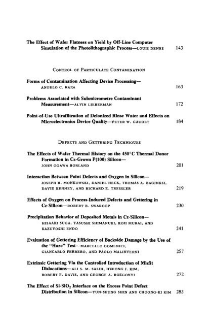
The Effect of Wafer Flatness on Yield by Off-line Computer<br />
Simulation of the Photolithographic Process—LOUIS DENES 143<br />
CONTROL OF PARTICULATE CONTAMINATION<br />
Forms of Contamination Affecting Device <strong>Processing</strong>—<br />
ANGELO C. RAPA 163<br />
Problems Associated with Submicrometre Contaminant<br />
Measurement—ALVIN LIEBERMAN 172<br />
Point-of-Use Ultrafiltration of Deionized Rinse Water and Effects on<br />
Microelectronics Device Quality—PETER W. GAUDET 184<br />
DEFECTS AND GETTERING TECHNIQUES<br />
The Effects of Wafer Thermal History on the 450°C Thermal Donor<br />
Formation in Cz-Grown P(IOO) Silicon—<br />
JOHN OGAWA BORLAND 201<br />
Interaction Between Point Defects and Oxygen in Silicon—<br />
JOSEPH R. MONKOWSKI, DANIEL HECK, THOMAS A. BAGINKSI,<br />
DAVID KENNEY, AND RICHARD E. TRESSLER 219<br />
Effects of Oxygen on Process-Induced Defects and Gettering in<br />
Cz-Silicon—ROBERT B. SWAROOP 230<br />
Precipitation Behavior of Deposited Metals in Cz-Silicon—<br />
HISAAKI SUGA, YASUSHI SHIMANUKI, KOJI MURAI, AND<br />
KAZUYOSHI ENDO 241<br />
Evaluation of Gettering Efficiency of Backside Damage by the Use of<br />
the "Haze" Test—MARCELLO DOMENICI,<br />
GIANCARLO FERRERO, AND PAOLO MALINVERNI 257<br />
Extrinsic Gettering Via the Controlled Introduction of Misfit<br />
Dislocations—ALI S. M. SALIH, HYEONG J. KIM,<br />
ROBERT F. DAVIS, AND GEORGE A. ROZGONYI 272<br />
The Effect of Si-SiOj Interface on the Excess Point Defect<br />
Distribution in Silicon—YUN-SEUNG SHIN AND CHOONG-KI KIM 283