Wafer Inspection Equipment Market

Create successful ePaper yourself
Turn your PDF publications into a flip-book with our unique Google optimized e-Paper software.
<strong>Wafer</strong> <strong>Inspection</strong> <strong>Equipment</strong> <strong>Market</strong> 2026 Focus On Research<br />
Methodology, <strong>Market</strong> Dynamics<br />
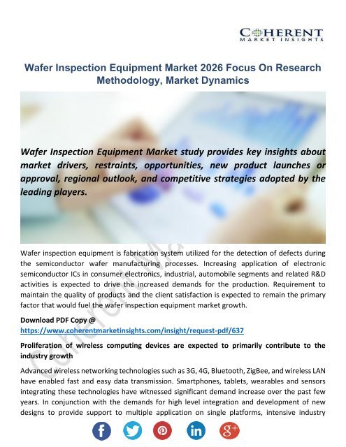
<strong>Wafer</strong> <strong>Inspection</strong> <strong>Equipment</strong> <strong>Market</strong> study provides key insights about<br />
market drivers, restraints, opportunities, new product launches or<br />
approval, regional outlook, and competitive strategies adopted by the<br />
leading players.<br />
<strong>Wafer</strong> inspection equipment is fabrication system utilized for the detection of defects during<br />
the semiconductor wafer manufacturing processes. Increasing application of electronic<br />
semiconductor ICs in consumer electronics, industrial, automobile segments and related R&D<br />
activities is expected to drive the increased demands for the production. Requirement to<br />
maintain the quality of products and the client satisfaction is expected to remain the primary<br />
factor that would fuel the wafer inspection equipment market growth.<br />
Download PDF Copy @<br />
https://www.coherentmarketinsights.com/insight/request-pdf/637<br />
Proliferation of wireless computing devices are expected to primarily contribute to the<br />
industry growth<br />
Advanced wireless networking technologies such as 3G, 4G, Bluetooth, ZigBee, and wireless LAN<br />
have enabled fast and easy data transmission. Smartphones, tablets, wearables and sensors<br />
integrating these technologies have witnessed significant demand increase over the past few<br />
years. In conjunction with the demands for high level integration and development of new<br />
designs to provide support to multiple application on single platforms, intensive industry
competition has led to increased demands for better quality and least defects in the<br />
semiconductor devices. Moreover, increasing demands for high performance chips for mission<br />
critical applications in industries and R&D activities will present considerable growth<br />
opportunities for the wafer inspection equipment market through the forecast period.<br />
IoT, and digitization are the major trends expected to transform the globe, which would require<br />
semiconductor technologies as the basis of their framework. Smart connected TVs, vehicle<br />
automation, kitchen automation, smart city, smart grids, are among the many such IoT concepts<br />
that are expected to gain traction over the next few years. This will increase demand for the<br />
electronic product manufacturing, which will in turn fuel the wafer inspection equipment<br />
market growth.<br />
<strong>Wafer</strong> <strong>Inspection</strong> <strong>Equipment</strong> <strong>Market</strong> Taxonomy<br />
On the basis of technology, the global wafer inspection equipment market is classified into:<br />
<br />
<br />
E-beam<br />
Optical<br />
On the basis of wafer type, the global wafer inspection equipment market is classified into:<br />
<br />
<br />
Unpatterned wafer<br />
Patterned wafer<br />
On the basis of end user, the global wafer inspection equipment market is classified into:<br />
<br />
<br />
<br />
Integrated device manufacturers<br />
Memory manufacturers<br />
Foundries<br />
Read more on research study @<br />
https://www.coherentmarketinsights.com/ongoing-insight/wafer-inspection-equipment-market-637<br />
Advent of 3D finFETs, NAND and advanced DRAMs technologies are expected to present<br />
considerable growth challenge to the industry growth<br />
Optical and E-beam are complementary technologies that perform distinct operations in the<br />
workflow. optical has fast throughputs and finds great applications in the end use. On the other<br />
hand E-beam helps in detection of smallest defects, however the throughputs are low. Owing
to these features, it finds substantial applications in R&D activities. Increasing demands for<br />
advanced computing and processing has led to development of 3D finFETs, NAND and advanced<br />
DRAMs, which requires the tools to assess complex structures. <strong>Wafer</strong> assessment on the scales<br />
below 10 nm is extremely difficult, and in case of overlooking of the smallest error can impact<br />
the end use. This is expected to be major industry growth challenge over the next coming years.<br />
Asia Pacific to be key growth engine of the wafer inspection equipment market<br />
Asia Pacific is the largest hub for the electronic semiconductor manufacturing activities, driven<br />
by the extensive production demands specifically in the countries that include China, Taiwan,<br />
Japan and South Korea. Moreover, the region is also attributed with the presence of key<br />
electronic industry participants such as Samsung, Sony, Toshiba, Panasonic, among many<br />
others, which will help the region sustain its dominance over the next few years.<br />
U.S. is expected to contribute to major industry share in the industry growth primarily owing to<br />
the major inclination of the users towards innovative technologies such as connected vehicles,<br />
industrial automation and other process automation. Moreover, the region is also characterized<br />
with the presence of major tech giants that include, Google, Tesla, Qualcomm, Texas<br />
Instruments, and GlobalFoundries among many others, which will provide consistent demands<br />
for the wafer inspection equipment market.<br />
Key players in the wafer inspection equipment market include Applied Materials, Zeiss Global,<br />
Hermes Microvision (ASML), FEI (Thermo Fisher Scientific), KLA-Tencor, Hitachi High-<br />
Technologies, JEOL, Lasec Corporation, Lam Research, Nikon, Nanometrics, Planar Corporation,<br />
Tokyo Seimitsu, Rudolph Technologies, and Toray Engineering.<br />
About Coherent <strong>Market</strong> Insights:<br />
Coherent <strong>Market</strong> Insights is a prominent market research and consulting firm offering actionready<br />
syndicated research reports, custom market analysis, consulting services, and competitive<br />
analysis through various recommendations related to emerging market trends, technologies,<br />
and potential absolute dollar opportunity.<br />
Contact Us:<br />
Mr. Shah<br />
Coherent <strong>Market</strong> Insights<br />
1001 4th Ave,
#3200<br />
Seattle, WA 98154<br />
Tel: +1-206-701-6702<br />
Email: sales@coherentmarketinsights.com