TVS Diode Arrays
TVS Diode Arrays
TVS Diode Arrays

You also want an ePaper? Increase the reach of your titles
YUMPU automatically turns print PDFs into web optimized ePapers that Google loves.
<strong>TVS</strong> <strong>Diode</strong> <strong>Arrays</strong><br />
Electronic Protection Array for ESD and Overvoltage Protection<br />
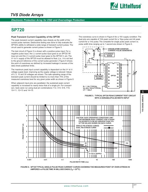
SP720<br />
Peak Transient Current Capability of the SP720<br />
The peak transient current capability rises sharply as the width of the<br />
current pulse narrows. Destructive testing was done to fully evaluate the<br />
SP720’s ability to withstand a wide range of transient current pulses. The<br />
circuit used to generate current pulses is shown in Figure 5.<br />
The test circuit of Figure 5 is shown with a positive pulse input. For a<br />
negative pulse input, the (-) current pulse input goes to an SP720 ‘IN’<br />
input pin and the (+) current pulse input goes to the SP720 V- pin. The<br />
V+ to V- supply of the SP720 must be allowed to float. (i.e., It is not tied<br />
to the ground reference of the current pulse generator.) Figure 6 shows<br />
the point of overstress as defined by increased leakage in excess of the<br />
data sheet published limits.<br />
The maximum peak input current capability is dependent on the V+ to Vvoltage<br />
supply level, improving as the supply voltage is reduced. Values<br />
of 0, 5, 15 and 30 voltages are shown. The safe operating range of the<br />
transient peak current should be limited to no more than 75% of the<br />
measured overstress level for any given pulse width as shown in Figure 6.<br />
When adjacent input pins are paralleled, the sustained peak current<br />
capability is increased to nearly twice that of a single pin. For comparison,<br />
tests were run using dual pin combinations 1+2, 3+4, 5+6, 7+9,<br />
10+11, 12+13 and 14+15.<br />
PEAK CURRENT (A)<br />
10<br />
9<br />
8<br />
7<br />
6<br />
5<br />
4<br />
3<br />
2<br />
1<br />
0<br />
0.001 0.01 0.1 1<br />
PULSE WIDTH TIME (ms)<br />
www.littelfuse.com<br />
The overstress curve is shown in Figure 6 for a 15V supply condition. The<br />
dual pins are capable of 10A peak current for a 10µs pulse and 4A peak<br />
current for a 1ms pulse. The complete for single pulse peak current vs.<br />
pulse width time ranging up to 1 second are shown in Figure 6.<br />
+<br />
VG -<br />
R 1<br />
VOLTAGE<br />
PROBE<br />
R1 ~ 10Ω TYPICAL<br />
VG ADJ. 10V/A TYPICAL<br />
C1 ~ 100µF<br />
(+)<br />
VARIABLE TIME DURATION<br />
CURRENT PULSE GENERATOR<br />
CURRENT<br />
SENSE<br />
1 IN V+ 16<br />
2 IN IN 15<br />
3 IN IN 14<br />
4<br />
5<br />
IN<br />
IN<br />
SP720<br />
IN<br />
IN<br />
13<br />
12<br />
6 IN IN 11<br />
7 IN IN 10<br />
8 V- IN 9<br />
FIGURE 5. TYPICAL SP720 PEAK CURRENT TEST CIRCUIT<br />
WITH A VARIABLE PULSE WIDTH INPUT<br />
CAUTION: SAFE OPERATING CONDITIONS LIMIT<br />
THE MAXIMUM PEAK CURRENT FOR A GIVEN<br />
PULSE WIDTH TO BE NO GREATER THAN 75%<br />
OF THE VALUES SHOWN ON EACH CURVE.<br />
SINGLE PIN STRESS CURVES<br />
DUAL PIN STRESS CURVE<br />
0V<br />
5V<br />
30V<br />
V+ TO V- SUPPLY<br />
10<br />
15V<br />
(-)<br />
15V<br />
C1<br />
100 1000<br />
FIGURE 6. SP720 TYPICAL SINGLE PULSE PEAK CURRENT CURVES SHOWING THE MEASURED POINT OF OVER-STRESS IN<br />
AMPERES vs PULSE TIME IN MILLISECONDS (T A = 25 o C)<br />
+<br />
-<br />
231<br />
5<br />
<strong>TVS</strong> DIODE ARRAYS