TVS Diode Arrays
TVS Diode Arrays
TVS Diode Arrays

Create successful ePaper yourself
Turn your PDF publications into a flip-book with our unique Google optimized e-Paper software.
5<br />
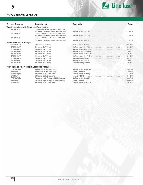
<strong>TVS</strong> <strong>Diode</strong> <strong>Arrays</strong><br />
Product Number Description Packaging Page<br />
<strong>TVS</strong> Protection with Filter and Termination<br />
SPUSB1AJT Upstream USB Port Terminator with ESD<br />
Suppression & EMI Filtering R1 = 12 ohms Surface Mount (SC70-6) . . . . . . . . . . . . . . . . . . . . . . . . . . . . . . . . . . . . . . . 217-219<br />
SPUSB1BJT Upstream USB Port Terminator With ESD<br />
Suppression & EMI Filtering R1 = 22 ohms Surface Mount (SC70-6) . . . . . . . . . . . . . . . . . . . . . . . . . . . . . . . . . . . . . . . 217-219<br />
SPUSB1CJT Upstream USB Port Terminator With ESD<br />
Suppression & EMI Filtering R1 = 33 ohms Surface Mount (SC70-6) . . . . . . . . . . . . . . . . . . . . . . . . . . . . . . . . . . . . . . . 217-219<br />
Avalanche <strong>Diode</strong> <strong>Arrays</strong><br />
SP0502BAHT 2 Channel SMT Array Surface Mount (SOT23). . . . . . . . . . . . . . . . . . . . . . . . . . . . . . . . . . . . . . . . 220-227<br />
SP0502BAJT 2 Channel SMT Array Surface Mount (SC70) . . . . . . . . . . . . . . . . . . . . . . . . . . . . . . . . . . . . . . . . . 220-227<br />
SP0503BAHT 3 Channel SMT Array Surface Mount (SOT143). . . . . . . . . . . . . . . . . . . . . . . . . . . . . . . . . . . . . . . 220-227<br />
SP0504BAAT 4 Channel SMT Array Surface Mount (TSSOP8) . . . . . . . . . . . . . . . . . . . . . . . . . . . . . . . . . . . . . . 220-227<br />
SP0504BAHT 4 Channel SMT Array Surface Mount (SOT23-5) . . . . . . . . . . . . . . . . . . . . . . . . . . . . . . . . . . . . . . 220-227<br />
SP0504BAJT 4 Channel SMT Array Surface Mount (SC70-5) . . . . . . . . . . . . . . . . . . . . . . . . . . . . . . . . . . . . . . . 220-227<br />
SP0505BAHT 5 Channel SMT Array Surfact Mount (SOT23-6). . . . . . . . . . . . . . . . . . . . . . . . . . . . . . . . . . . . . . . 220-227<br />
SP0505BAJT 5 Channel SMT Array Surface Mount (SC70-6) . . . . . . . . . . . . . . . . . . . . . . . . . . . . . . . . . . . . . . . 220-227<br />
SP0506BAAT 6 Channel SMT Array Surfact Mount (MSOP8). . . . . . . . . . . . . . . . . . . . . . . . . . . . . . . . . . . . . . . . 220-227<br />
High Voltage Rail Clamp SCR/<strong>Diode</strong> <strong>Arrays</strong><br />
SP720AB (T) 14 Channel SCR/<strong>Diode</strong> Array Surface Mount (SOIC16) . . . . . . . . . . . . . . . . . . . . . . . . . . . . . . . . . . . . . . . 228-233<br />
SP720AP 14 Channel SCR/<strong>Diode</strong> Array Leaded (PDIP16) . . . . . . . . . . . . . . . . . . . . . . . . . . . . . . . . . . . . . . . . . . . . . 228-233<br />
SP721AB (T) 6 Channel SCR/<strong>Diode</strong> Array Surface Mount (SOIC8) . . . . . . . . . . . . . . . . . . . . . . . . . . . . . . . . . . . . . . . . 234-239<br />
SP721AP 6 Channel SCR/<strong>Diode</strong> Array Leaded (PDIP8) . . . . . . . . . . . . . . . . . . . . . . . . . . . . . . . . . . . . . . . . . . . . . . 234-239<br />
SP723AB (T) 6 Channel High Energy SCR/<strong>Diode</strong> Array Surface Mount (SOIC8) . . . . . . . . . . . . . . . . . . . . . . . . . . . . . . . . . . . . . . . . 240-245<br />
SP723AP 6 Channel High Energy SCR/<strong>Diode</strong> Array Leaded (PDIP8) . . . . . . . . . . . . . . . . . . . . . . . . . . . . . . . . . . . . . . . . . . . . . . 240-245<br />
SP724AHT 4 Channel SCR <strong>Diode</strong> Array Surface Mount (SOT23-6) . . . . . . . . . . . . . . . . . . . . . . . . . . . . . . . . . . . . . . 246-251<br />
216<br />
www.littelfuse.com
<strong>TVS</strong> <strong>Diode</strong> <strong>Arrays</strong><br />
Upstream USB Port Terminator with ESD Suppression & EMI Filtering<br />
SPUSB1 Series<br />
The Littelfuse SPUSB1 Series is a multifunctional USB port protection<br />
network designed to provide ESD protection, EMI/RFI filtering and line<br />
termination for a single USB 1.1 port. The SPUSB1 can replace a minimum<br />
of ten typically larger “discrete” devices resulting in inventory and<br />
placement cost savings.<br />
The SPUSB1 Series combines Transient Voltage Suppression (<strong>TVS</strong>)<br />
avalanche diodes, EMI/RFI filtering components (R1 and C1), and<br />
a1.5kΩ termination resistor (R2). The filtering components are included<br />
to satisfy recommendations in the USB 1.1 specification, and the 1.5kΩ<br />
resistor (R2) is included as a pull-up resistor to VBUS.<br />
The SPUSB1 Series can be used for termination and protection<br />
of“upstream” USB devices such as PDAs, digital cameras, scanners and<br />
hubs which are often at risk from transient voltage surges and<br />
electromagnetic interference from both internal and external sources.<br />
To support a wide range of circuit conditions, Littelfuse offers three<br />
resistance values for the series resistor (R1). The series resistance plus<br />
the USB driver output resistance must be close to the USB cable’s characteristic<br />
impedance of 45Ω (90Ω balanced) to minimize transmission<br />
line reflections.<br />
Circuit Diagram<br />
Ordering Information<br />
PART<br />
NUMBER<br />
SPUSB1AJT<br />
SPUSB1BJT<br />
SPUSB1CJT<br />
1<br />
2<br />
GND<br />
3<br />
R1 (Ohm)<br />
12<br />
22<br />
33<br />
C1<br />
C1<br />
SC70-6<br />
R1<br />
R1<br />
R2 (KOhm)<br />
1.5<br />
1.5<br />
1.5<br />
R2<br />
V BUS<br />
6<br />
5<br />
4<br />
C1 (pF)<br />
47<br />
47<br />
47<br />
DEVICE<br />
BRAND<br />
UFA<br />
UFB<br />
UFC<br />
Features<br />
www.littelfuse.com<br />
• One upstream USB port terminator, EMI filter and transient<br />
overvoltage protector in a single surface-mount package<br />
• Compact SC70 package saves board space and lowers<br />
manufacturing costs compared to discrete solutions<br />
• ESD protection to 30kV contact discharge per MIL-STD- 883D,<br />
method 3015<br />
• ESD protection to 15kV contact discharge per IEC 61000-4-2<br />
international standard<br />
Applications<br />
• Desktop/Laptop PCs<br />
• USB peripherals (printers, scanners, zip drives)<br />
• PDAs / wireless handsets<br />
• Digital cameras<br />
• MP3 Players<br />
• Cable Modems<br />
PKG<br />
TYPE<br />
SC70-6<br />
SC70-6<br />
SC70-6<br />
#/REEL<br />
3000<br />
3000<br />
3000<br />
217<br />
5<br />
<strong>TVS</strong> DIODE ARRAYS
<strong>TVS</strong> <strong>Diode</strong> <strong>Arrays</strong><br />
Upstream USB Port Terminator with ESD Suppression & EMI Filtering<br />
SPUSB1 Series<br />
218<br />
Supply Voltage VBUS<br />
DC Power per Resistor<br />
Package Power<br />
Temperature Range:<br />
Operating<br />
Storage<br />
Absolute Maximum Ratings<br />
Parameter Rating Unit<br />
5.5<br />
100<br />
200<br />
-40 to +85<br />
-65 to +150<br />
Standard<br />
Specifications<br />
(at 25°C unless specified otherwise)<br />
Parameter MIN TYP MAX Unit<br />
Resistance R1 (SPUSB1AJT only)<br />
6% 12 14% Ω<br />
Resistance R1 (SPUSB1CJT only)<br />
26% 33 40% Ω<br />
Resistance R1 (SPUSB1BJT only)<br />
18% 22 26% Ω<br />
Resistance R2<br />
1.2% 1.5 18% kΩ<br />
Capacitance C1 @ 2.5 v DC, 1MHz<br />
38% 47 56% pF<br />
<strong>Diode</strong> Leakage at 3.3V<br />
1 100 nA<br />
<strong>Diode</strong> Reverse Bias Stand-off Voltage, 1= 10µA<br />
Signal Clamp Voltage:<br />
5.5<br />
V<br />
Positive Clamp, 10mA<br />
5.6 6.8 8.0 V<br />
Negative Clamp, 10mA<br />
(1)<br />
In-system ESD Withstand Voltage<br />
-1.2 -0.8 -0.4 V<br />
Human Body Model (MIL-STD-883D, method 3015<br />
±30<br />
kV<br />
IEC 81000-4-2, contact discharge method (I/O pins)<br />
±15<br />
kV<br />
IEC 81000-4-2, contact discharge method (V<br />
BUS<br />
pin)<br />
±25<br />
kV<br />
(1)<br />
Clamping Voltage During ESD Discharge<br />
Positive<br />
10<br />
V<br />
MIL-STD-883D (Method 3015), 8kV<br />
Note:<br />
Negative<br />
-5<br />
V<br />
(1) ESD applied to input/outputV DD pins with respect to GND, one at a time.<br />
Clamping Voltage is measured at the opposite side of the EMI filter to the ESD pin (ie: if ESD is applied to pin1 then clamping<br />
voltage is measured at pin 6). Unused pins are open.<br />
These parameters guaranteed by design.<br />
APPLICATIONS INFORMATION<br />
D+<br />
USB 1.1<br />
CONTROLLER<br />
IC<br />
GND<br />
D-<br />
1<br />
D1<br />
2<br />
GND<br />
3<br />
C1<br />
C1<br />
R1<br />
R1<br />
R2<br />
D4<br />
D2 D3<br />
6<br />
5<br />
V BUS<br />
4<br />
3.3V<br />
D+<br />
USB 1.1<br />
CONNECTOR<br />
Figure 1. Full-Speed Devices (12Mbits per second)<br />
For full speed operation the pull-up resistor R2 is connected to the D+ pin.<br />
D-<br />
D-<br />
USB 1.1<br />
CONTROLLER<br />
IC<br />
GND<br />
D+<br />
www.littelfuse.com<br />
1<br />
D1<br />
2<br />
GND<br />
3<br />
V<br />
mW<br />
mW<br />
° C<br />
C1<br />
C1<br />
R1<br />
R1<br />
R2<br />
D4<br />
D2 D3<br />
6<br />
5<br />
V BUS<br />
4<br />
3.3V<br />
D-<br />
USB 1.1<br />
CONNECTOR<br />
Figure 2. Low-Speed Devices (1.5Mbits per second)<br />
Low speed connection requires the pull-up resistor R2 to be connected to the Dpin.<br />
Please note the reversal of the D- and D+ pins on Figure 2 versus Figure 1.<br />
D+
<strong>TVS</strong> <strong>Diode</strong> <strong>Arrays</strong><br />
Upstream USB Port Terminator with ESD Suppression & EMI Filtering<br />
SPUSB1 Series<br />
PACKAGING INFORMATION<br />
Lead Plating<br />
Mechanical Specifications<br />
Tin-Lead<br />
Lead Material Copper Alloy<br />
Lead Coplanarity 0.004 inches (0.102mm)<br />
Subsitute Material Silicon<br />
Body Material Molded Epoxy<br />
Flammability UL94-V-0<br />
c<br />
Outline Drawings<br />
6<br />
1 2 3<br />
B<br />
B<br />
D<br />
5<br />
B<br />
4<br />
A1<br />
E HE<br />
A2 A<br />
L<br />
T<br />
P<br />
SPUSB1AJT - SC70-6<br />
SPUSB1BJT - SC70-6<br />
SPUSB1CJT - SC70-6<br />
Recommended Pad Layout<br />
S (REF)<br />
+ + +<br />
+<br />
O (REF)<br />
+ + +<br />
R<br />
N (REF)<br />
M (REF)<br />
www.littelfuse.com<br />
Package<br />
Pins<br />
JEDEC<br />
A<br />
A1<br />
A2<br />
B<br />
c<br />
D<br />
E<br />
e<br />
HE<br />
L<br />
M<br />
N<br />
O<br />
P<br />
R<br />
S<br />
T<br />
mm<br />
SC70-6<br />
6<br />
MO-203 Issue A<br />
inches<br />
min max min max<br />
0.80 1.10 0.031 0.043<br />
0.00 0.10 0.000 0.004<br />
0.70 1.00 0.028 0.039<br />
0.15 0.30 0.006 0.012<br />
0.08 0.25 0.003 0.010<br />
1.85 2.25 0.073 0.089<br />
1.15 1.35 0.045 0.053<br />
0.65 BSC 0.026 BSC<br />
2.00 2.40<br />
0.26 0.46<br />
PD@70°C 0.2W<br />
# / bag 1000 pcs<br />
# / tape & reel 3,000 pcs<br />
*See device brand for marking information.<br />
0.079 0.094<br />
0.010 0.018<br />
- 1.60 - 0.063<br />
- 1.30 - 0.052<br />
- 0.65 - 0.026<br />
- 0.70 - 0.058<br />
- 0.35 - 0.014<br />
- 0.90 - 0.035<br />
- 2.50 - 0.098<br />
219<br />
5<br />
<strong>TVS</strong> DIODE ARRAYS
<strong>TVS</strong> <strong>Diode</strong> <strong>Arrays</strong><br />
Surface Mount <strong>TVS</strong> Avalanche <strong>Diode</strong> Array<br />
SP0502BA, SP0503BA, SP0504BA, SP0505BA, SP0506BA<br />
The surface mount family of arrays are designed to suppress ESD and<br />
other transient overvoltage events. These arrays are used to meet the<br />
International Electrotechnical Compatibility (IEC transient immunity standards<br />
IEC 61000-4-2 for Electrostatic Discharge Requirements). The<br />
series are used to help protect sensitive digital or analog input circuits<br />
on data, signal, or control lines with voltage levels up to 5VDC.<br />
The monolithic silicon arrays are comprised of specially designed<br />
structures for transient voltage suppression(<strong>TVS</strong>). The size and<br />
shape of these structures have be tailored for transient protection.<br />
The low capacitance and clamp voltage are ideal for high speed<br />
signal line protection.<br />
Ordering Information<br />
Part Number<br />
SP0502BAHT<br />
SP0503BAHT<br />
SP0504BAHT<br />
SP0505BAHT<br />
SP0504BAAT<br />
SP0506BAAT<br />
SP0502BAJT<br />
SP0504BAJT<br />
SP0505BAJT<br />
Pinout<br />
SP0502BAHT<br />
SP0502BAJT<br />
1<br />
1<br />
2<br />
SP0505BAHT<br />
SP0505BAJT<br />
2<br />
3 4<br />
220<br />
6<br />
3<br />
5<br />
CH<br />
2<br />
3<br />
4<br />
5<br />
4<br />
6<br />
2<br />
4<br />
5<br />
1<br />
Package Type<br />
SOT23<br />
SOT143<br />
SOT23-5<br />
SOT23-6<br />
TSSOP-8<br />
MSOP-8<br />
SC70-3<br />
SC70-5<br />
SC70-6<br />
SP0503BAHT<br />
4<br />
2 3<br />
SP0504BAAT<br />
8 7 6 5<br />
1<br />
2<br />
3<br />
4<br />
Quantity Per<br />
Reel<br />
3000<br />
3000<br />
3000<br />
3000<br />
4000<br />
4000<br />
3000<br />
3000<br />
3000<br />
SP0504BAHT<br />
SP0504BAJT<br />
1<br />
2<br />
3 4<br />
SP0506BAAT<br />
8 7 6 5<br />
1<br />
2<br />
3<br />
4<br />
5<br />
Features<br />
www.littelfuse.com<br />
• An Array of 2, 3, 4, 5 or 6 <strong>TVS</strong> Avalanche <strong>Diode</strong>s in a ultra small<br />
SC70, SOT-23, SOT-143, MSOP or TSSOP packages<br />
• ESD Capability Standards<br />
IEC 61000-4-2, Direct Discharge . . . . . . . . . 20kV (Level 4)<br />
IEC 61000-4-2, Air Discharge . . . . . . . . . . . 30kV (Level 4)<br />
MIL STD 883 3015.7 . . . . . . . . . . . . . . . . . . . . . . . . . . 30kV<br />
• Input Protection for Applications Up to 5VDC<br />
• Fast Response Time . . . . . . . . . . . . . . . . . . . . . . . . . . . < 1ns<br />
• Low Input Capacitance . . . . . . . . . . . . . . . . . . . . 30pF Typical<br />
• Operating Temperature Range. . . . . . . . . . . . . -40°C to 85°C<br />
Applications<br />
• Mobile phone handsets<br />
• Personal Digital Assistants (PDA)<br />
• Portable handheld equipment (Laptop, Palmtop computers)<br />
• Computer port, keyboard (USB1.1)<br />
• Digital still cameras<br />
• Digital video cameras<br />
• MP3 players
<strong>TVS</strong> <strong>Diode</strong> <strong>Arrays</strong><br />
Surface Mount <strong>TVS</strong> Avalanche <strong>Diode</strong> Array<br />
SP0502BA, SP0503BA, SP0504BA, SP0505BA, SP0506BA<br />
Electrical Specifications TA = -25°C, Unless Otherwise Specified<br />
PARAMETER<br />
TEST CONDITIONS MIN<br />
TYPICAL MAX<br />
Reverse Standoff Voltage<br />
I = 10µA<br />
5.5<br />
-<br />
-<br />
Reverse Standoff Leakage Current<br />
Signal Clamp Voltage<br />
V = 5.0V<br />
1<br />
100<br />
Positive<br />
I = 10mA<br />
5.6<br />
6.8<br />
8<br />
Negative<br />
Clamp Voltage during ESD<br />
MIL-STD-883 Method 3015 (HBM) test<br />
I = 10mA<br />
-1.2<br />
-0.8<br />
-0.4<br />
8kV<br />
12<br />
8kV<br />
ESD Test Level (1)<br />
-8<br />
IEC-61000-2, Contact discharge<br />
20<br />
MIL-STD-883 Method 3015 (HBM)<br />
30<br />
Capacitance<br />
2.5V @ 1Mhz<br />
30<br />
Turn on/off Time<br />
Temperature Range<br />
<strong>TVS</strong> <strong>Diode</strong> <strong>Arrays</strong><br />
Input Current (A)<br />
Surface Mount <strong>TVS</strong> Avalanche <strong>Diode</strong> Array<br />
SP0502BA, SP0503BA, SP0504BA, SP0505BA, SP0506BA<br />
Typical Input VI Characteristics<br />
(Pulse-mode measurements, pulse width = 0.7 mS nominal)<br />
1.6<br />
1.4<br />
1.2<br />
1.0<br />
0.8<br />
0.6<br />
0.4<br />
0.2<br />
0.0<br />
-0.2<br />
-0.4<br />
-0.6<br />
-0.8<br />
-1.0<br />
-1.2<br />
-1.4<br />
-1.6<br />
-3 -2 -1 0 1 2 3 4 5 6 7 8 9<br />
Input Voltage (V)<br />
Package Information<br />
222<br />
Mechanical Specifications<br />
Lead Plating Tin-Lead<br />
Lead Material Copper Alloy<br />
Lead Coplanarity 0.004 inches (0.102mm)<br />
Subsitute Material Silicon<br />
Body Material Molded Epoxy<br />
Flammability UL94-V-0<br />
Notes:<br />
1. All dimensions are in millimeters.<br />
2. Dimensions include solder plating.<br />
3. Dimensions are exclusive of mold flash & metal burr.<br />
4. All specifications comply to JEDEC SPEC MO-203 ISSUE A.<br />
5. Blo is facing up for mold and facing down for trim/form,<br />
i.e. reverse trim/form.<br />
6. Package surface matte finish VDI 11-13.<br />
www.littelfuse.com<br />
<strong>Diode</strong> Capacitance (pF)<br />
Typical <strong>Diode</strong> Capacitance<br />
vs. Reverse Voltage<br />
60<br />
40<br />
20<br />
0<br />
0 1 2 3 4 5<br />
<strong>Diode</strong> Reverse Voltage (V)
<strong>TVS</strong> <strong>Diode</strong> <strong>Arrays</strong><br />
Surface Mount <strong>TVS</strong> Avalanche <strong>Diode</strong> Array<br />
SP0502BA, SP0503BA, SP0504BA, SP0505BA, SP0506BA<br />
C<br />
c<br />
e<br />
B<br />
3<br />
502<br />
1 2<br />
D<br />
e<br />
e<br />
5 4<br />
1 2 3<br />
B<br />
Outline Drawings<br />
e<br />
504<br />
D<br />
E<br />
A1<br />
HE<br />
A2 A<br />
A1<br />
L<br />
E HE<br />
A2 A<br />
L<br />
SP0502BAJT - SC70-3<br />
SP0504BAJT - SC70-5<br />
www.littelfuse.com<br />
Package<br />
Pins<br />
JEDEC<br />
A<br />
A1<br />
A2<br />
B<br />
c<br />
D<br />
E<br />
e<br />
HE<br />
L<br />
Package<br />
Pins<br />
JEDEC<br />
A<br />
A1<br />
A2<br />
B<br />
c<br />
D<br />
E<br />
e<br />
HE<br />
L<br />
mm<br />
SC70-3<br />
3<br />
MO-203 Issue A<br />
inches<br />
min max min max<br />
0.80 1.10 0.031 0.043<br />
0.00 0.10 0.00 0.004<br />
0.70 1.00 0.028 0.039<br />
0.15 0.30 0.006 0.012<br />
0.08 0.25 0.003 0.010<br />
1.85 2.25 0.073 0.089<br />
1.15 1.35 0.045 0.053<br />
0.66 BSC 0.026 BSC<br />
2.00 2.40<br />
0.26 0.46<br />
mm<br />
SC70-5<br />
5<br />
MO-203 Issue A<br />
inches<br />
min max min max<br />
0.80 1.10 0.03 0.043<br />
0.00 0.10 0.00 0.004<br />
0.70 1.00 0.028 0.039<br />
0.15 0.30 0.006 0.012<br />
0.08 0.25 0.003 0.010<br />
1.85 2.25 0.073 0.089<br />
1.15 1.35 0.045 0.053<br />
0.65 BSC 0.026 BSC<br />
2.00 2.40<br />
0.26 0.46<br />
0.079 0.094<br />
0.010 0.018<br />
0.079 0.094<br />
0.010 0.018<br />
223<br />
5<br />
<strong>TVS</strong> DIODE ARRAYS
<strong>TVS</strong> <strong>Diode</strong> <strong>Arrays</strong><br />
Surface Mount <strong>TVS</strong> Avalanche <strong>Diode</strong> Array<br />
SP0502BA, SP0503BA, SP0504BA, SP0505BA, SP0506BA<br />
c<br />
Outline Drawings<br />
C<br />
6<br />
1 2 3<br />
B<br />
e<br />
224<br />
D<br />
5<br />
e<br />
505<br />
e<br />
b<br />
3<br />
e1<br />
4<br />
502B<br />
1 2<br />
D<br />
A1<br />
E HE<br />
A2 A<br />
E1<br />
A1<br />
L1<br />
L<br />
E<br />
A<br />
T<br />
P<br />
P<br />
SP0505BAJT - SC70-6<br />
Recommended Pad Layout<br />
S (REF)<br />
+ + +<br />
SP0502BAHT - SOT23<br />
Recommended Pad Layout<br />
0<br />
+<br />
O (REF)<br />
+ + +<br />
R<br />
N (REF)<br />
M<br />
N<br />
M (REF)<br />
www.littelfuse.com<br />
Package<br />
Pins<br />
JEDEC<br />
A<br />
A1<br />
A2<br />
B<br />
c<br />
D<br />
E<br />
e<br />
HE<br />
L<br />
M<br />
N<br />
O<br />
P<br />
R<br />
S<br />
T<br />
Package<br />
Pins<br />
JEDEC<br />
A<br />
A1<br />
b<br />
c<br />
D<br />
E<br />
E1<br />
e<br />
e1<br />
L1<br />
M<br />
N<br />
O<br />
P<br />
mm<br />
SC70-6<br />
5<br />
MO-203 Issue A<br />
inches<br />
min max min max<br />
0.80 1.10 0.031 0.043<br />
0.00 0.10 0.00 0.004<br />
0.70 1.00 0.028 0.039<br />
0.15 0.30 0.006 0.012<br />
0.08 0.25 0.003 0.010<br />
1.85 2.25 0.073 0.089<br />
1.15 1.35 0.045 0.053<br />
0.65 BSC 0.026 BSC<br />
2.00 2.40<br />
0.26 0.46<br />
-<br />
-<br />
-<br />
-<br />
-<br />
-<br />
-<br />
1.60<br />
1.30<br />
0.65<br />
0.70<br />
0.35<br />
0.90<br />
2.50<br />
0.079 0.094<br />
0.010 0.018<br />
- 0.063<br />
- 0.052<br />
- 0.026<br />
- 0.058<br />
- 0.014<br />
- 0.035<br />
- 0.098<br />
SOT23<br />
3<br />
TO-236<br />
mm inches<br />
min max min max<br />
0.89 1.12 0.035 0.044<br />
0.01 0.1 0.0004 0.004<br />
0.3 0.5 0.012 0.020<br />
0.08 0.2 0.003 0.008<br />
2.8 3.04 0.110 0.120<br />
2.1 2.64 0.083 0.104<br />
1.2 1.4 0.047 0.055<br />
0.95 BSC 0.95 BSC<br />
1.90 BSC 1.90 BSC<br />
0.54 REF 0.54 REF<br />
2.29 .090<br />
0.95 .0375<br />
0.78 .030TYP<br />
0.78 .030TYP
<strong>TVS</strong> <strong>Diode</strong> <strong>Arrays</strong><br />
Surface Mount <strong>TVS</strong> Avalanche <strong>Diode</strong> Array<br />
SP0502BA, SP0503BA, SP0504BA, SP0505BA, SP0506BA<br />
e1<br />
c<br />
Outline Drawings<br />
c<br />
4<br />
e<br />
503B<br />
1 2<br />
D<br />
e1<br />
e<br />
5 4<br />
504B<br />
1 2 3<br />
D<br />
3<br />
B<br />
A1<br />
E1<br />
b2 b A1<br />
L1<br />
L<br />
E1 E<br />
L1<br />
A<br />
A<br />
E<br />
3.40 (.134")<br />
3.60 (.140")<br />
SP0504BAHT - SOT23-5<br />
P<br />
SP0503BAHT - SOT143<br />
Recommended Pad Layout<br />
0.80 (.032")<br />
1.00 (.040")<br />
2.20<br />
(.087")<br />
REF<br />
Recommended Pad Layout<br />
O<br />
1.90<br />
(.075")<br />
1.70<br />
(.067")<br />
BSC<br />
1.00 (.040")<br />
1.20 (.048")<br />
N<br />
0.80 (.032")<br />
1.00 (.040")<br />
1.40 (.055")<br />
MAX<br />
M<br />
www.littelfuse.com<br />
Package<br />
Pins<br />
JEDEC<br />
A<br />
A1<br />
b<br />
b2<br />
c<br />
D<br />
E<br />
E1<br />
e<br />
e1<br />
L<br />
L1<br />
Package<br />
Pins<br />
JEDEC<br />
A<br />
A1<br />
b<br />
c<br />
D<br />
E<br />
E1<br />
e<br />
e1<br />
L1<br />
M<br />
N<br />
O<br />
P<br />
SOT143<br />
4<br />
TO-253<br />
mm inches<br />
min max min max<br />
0.08 1.22 0.031 0.048<br />
0.05 0.15 0.002 0.006<br />
0.30 0.50 0.012 0.019<br />
0.76 0.89 0.030 0.035<br />
0.08 0.20 0.003 0.008<br />
2.80 3.04 0.110 0.119<br />
2.10 2.64 0.082 0.103<br />
1.20 1.40 0.047 0.055<br />
1.92 BSC 0.076 BSC<br />
0.20 BSC 0.008 BSC<br />
0.4 0.6 0.016 0.024<br />
0.550 REF 0.022 REF<br />
SOT23-5<br />
5<br />
MO-178<br />
mm inches<br />
min max min max<br />
- 1.45 - 0.057<br />
0 0.15 0 0.006<br />
0.3 0.5 0.012 0.020<br />
0.08 0.22 0.003 0.009<br />
2.75 3.05 0.108 0.120<br />
2.6 3.0 0.102 0.118<br />
1.45 1.75 0.057 0.069<br />
0.95 BSC 0.95 BSC<br />
1.90 BSC 1.90 BSC<br />
0.60 REF 0.60 REF<br />
2.59 .102<br />
0.95 .038<br />
0.69 .027TYP<br />
0.99 .039TYP<br />
225<br />
5<br />
<strong>TVS</strong> DIODE ARRAYS
<strong>TVS</strong> <strong>Diode</strong> <strong>Arrays</strong><br />
Surface Mount <strong>TVS</strong> Avalanche <strong>Diode</strong> Array<br />
SP0502BA, SP0503BA, SP0504BA, SP0505BA, SP0506BA<br />
Outline Drawings<br />
c<br />
E<br />
A<br />
L2<br />
6<br />
226<br />
e1<br />
e<br />
5<br />
505B<br />
1 2 3<br />
A1<br />
b<br />
D<br />
D<br />
4<br />
A1<br />
LF<br />
504 BA<br />
B<br />
E1 E<br />
L1<br />
A<br />
C<br />
L1<br />
E1<br />
SP0505BAHT - SOT23-6<br />
P<br />
Recommended Pad Layout<br />
O<br />
N<br />
M<br />
www.littelfuse.com<br />
Package<br />
Pins<br />
JEDEC<br />
A<br />
A1<br />
b<br />
c<br />
D<br />
E<br />
E1<br />
e<br />
e1<br />
L1<br />
M<br />
N<br />
O<br />
P<br />
SOT23-6<br />
6<br />
MO-178<br />
mm inches<br />
min max min max<br />
- 1.45 - 0.057<br />
0 0.15 0 0.006<br />
0.3 0.5 0.012 0.020<br />
0.08 0.22 0.003 0.009<br />
2.75 3.05 0.108 0.120<br />
2.6 3.0 0.102 0.118<br />
1.45 1.75 0.057 0.069<br />
0.95 BSC 0.95 BSC<br />
1.90 BSC 1.90 BSC<br />
0.60 REF 0.60 REF<br />
PD@70°C .225W<br />
SP0504BAAT - TSSOP-8 Package TSSOP-8<br />
D<br />
E<br />
E1<br />
A<br />
A1<br />
B<br />
C<br />
L1<br />
L2<br />
2.59 .102<br />
0.95 0.038<br />
0.69 .027TYP<br />
0.99 .039TYP<br />
mm inches<br />
min max min max<br />
2.90 3.10 .144 .122<br />
6.40 REF .252 REF<br />
4.29 4.50 .17 .18<br />
1.194 REF .047 REF<br />
0.051 0.152 .002 0.006<br />
- 0.30 - .12TYP<br />
- 0.66 - .26TYP<br />
0.51 0.76 .020 .030<br />
0.102 0.203 .004 .008
<strong>TVS</strong> <strong>Diode</strong> <strong>Arrays</strong><br />
Surface Mount <strong>TVS</strong> Avalanche <strong>Diode</strong> Array<br />
SP0502BA, SP0503BA, SP0504BA, SP0505BA, SP0506BA<br />
E<br />
Outline Drawings<br />
A<br />
A1<br />
L1<br />
D<br />
LF<br />
506 B<br />
B<br />
E1<br />
C<br />
L2<br />
SP0506BAAT - MSOP-8<br />
Recommended Pad Layout<br />
F<br />
G<br />
I<br />
H<br />
F1<br />
www.littelfuse.com<br />
Package MSOP-8<br />
mm inches<br />
min max min max<br />
D 2.90 3.10 .144 .122<br />
E 4.78 4.98 .188 .196<br />
E1 2.90 3.10 .114 .122<br />
A 0.87 1.17 .034 .046<br />
A1 0.05 0.25 .002 0.10<br />
B<br />
- 0.30TYP - .12TYP<br />
C<br />
- 0.65TYP - .25TYP<br />
L1 0.52 0.54 .017 .025<br />
L2<br />
- 0.18TYP - .007TYP<br />
F<br />
- 5.28 - .208<br />
F1<br />
- 4.24 - .167<br />
G<br />
- 0.65 - .0256<br />
H<br />
- 0.38 - .015<br />
I<br />
- 1.04<br />
- .041<br />
227<br />
5<br />
<strong>TVS</strong> DIODE ARRAYS
<strong>TVS</strong> <strong>Diode</strong> <strong>Arrays</strong><br />
Electronic Protection Array for ESD and Overvoltage Protection<br />
SP720<br />
The SP720 is an array of SCR/<strong>Diode</strong> bipolar structures for ESD and<br />
over-voltage protection to sensitive input circuits. The SP720 has 2<br />
protection SCR/<strong>Diode</strong> device structures per input. A total of 14 available<br />
inputs can be used to protect up to 14 external signal or bus lines.<br />
Over-voltage protection is from the IN (pins 1-7 and 9-15) to V+ or V-.<br />
The SCR structures are designed for fast triggering at a threshold of one<br />
+VBE diode threshold above V+ (Pin 16) or a -VBE diode threshold<br />
below V- (Pin 8). From an IN input, a clamp to V+ is activated if a transient<br />
pulse causes the input to be increased to a voltage level greater<br />
than one VBE above V+. A similar clamp to V- is activated if a negative<br />
pulse, one VBE less than V-, is applied to an IN input. Standard ESD<br />
Human Body Model (HBM) Capability is:<br />
HBM STANDARD MODE R C ESD (V)<br />
IEC 61000-4-2 Air 330Ω 150pF >15kV<br />
Refer to Figure 1 and Table 1 for further detail. Refer to Application Note<br />
AN9304 and AN9612 for additional information.<br />
Ordering Information<br />
228<br />
Direct 330Ω 150pF >4kV<br />
Direct, Dual Pins 330Ω 150pF >8kV<br />
MIL-STD-3015.7 Direct, In-circuit 1.5kΩ 100pF >15kV<br />
TEMP. RANGE<br />
PART NO. ( o PKG. Min.<br />
C) PACKAGE NO. Order<br />
SP720AP -40 to 105 16 Ld PDIP E16.3 1500<br />
SP720AB -40 to 105 16 Ld SOIC M16.15 1970<br />
SP720ABT -40 to 105 16 Ld SOIC<br />
Tape and Reel<br />
M16.15 2500<br />
Pinout<br />
SP720 (PDIP, SOIC)<br />
IN<br />
IN<br />
IN<br />
IN<br />
IN<br />
IN<br />
IN<br />
V-<br />
1<br />
2<br />
3<br />
4<br />
5<br />
6<br />
7<br />
8<br />
TOP VIEW<br />
16<br />
15<br />
14<br />
13<br />
12<br />
11<br />
10<br />
9<br />
V+<br />
IN<br />
IN<br />
IN<br />
IN<br />
IN<br />
IN<br />
IN<br />
Features<br />
www.littelfuse.com<br />
• ESD Interface Capability for HBM Standards<br />
- MIL STD 3015.7. . . . . . . . . . . . . . . . . . . . . . . . . . . . . . . . . . . 15kV<br />
- IEC 61000-4-2, Direct Discharge,<br />
Single Input . . . . . . . . . . . . . . . . . . . . . . . . . . . . . . . . 4kV (Level 2)<br />
Two Inputs in Parallel . . . . . . . . . . . . . . . . . . . . . . . . 8kV (Level 4)<br />
- IEC 61000-4-2, Air Discharge. . . . . . . . . . . . . . . . . 15kV (Level 4)<br />
• High Peak Current Capability<br />
- IEC 61000-4-5 (8/20µs) . . . . . . . . . . . . . . . . . . . . . . . . . . . . . . ±3A<br />
- Single Pulse, 100µs Pulse Width. . . . . . . . . . . . . . . . . . . . . . . ±2A<br />
- Single Pulse, 4µs Pulse Width. . . . . . . . . . . . . . . . . . . . . . . . . ±5A<br />
• Designed to Provide Over-Voltage Protection<br />
- Single-Ended Voltage Range to . . . . . . . . . . . . . . . . . . . . . . +30V<br />
- Differential Voltage Range to. . . . . . . . . . . . . . . . . . . . . . . . . ±15V<br />
• Fast Switching . . . . . . . . . . . . . . . . . . . . . . . . . . . . . . . . . 2ns Risetime<br />
• Low Input Leakages . . . . . . . . . . . . . . . . . . . . . . . . . 1nA at 25 o C (Typ)<br />
• Low Input Capacitance . . . . . . . . . . . . . . . . . . . . . . . . . . . . . 3pF (Typ)<br />
• An Array of 14 SCR/<strong>Diode</strong> Pairs<br />
• Operating Temperature Range . . . . . . . . . . . . . . . . . . . . -40 o C to 105 o C<br />
Applications<br />
• Microprocessor/Logic Input Protection<br />
• Data Bus Protection<br />
• Analog Device Input Protection<br />
• Voltage Clamp<br />
Functional Block Diagram<br />
V+ 16<br />
IN<br />
V-<br />
1<br />
8<br />
IN<br />
2<br />
3 - 7<br />
9 - 15<br />
IN
<strong>TVS</strong> <strong>Diode</strong> <strong>Arrays</strong><br />
Electronic Protection Array for ESD and Overvoltage Protection<br />
SP720<br />
Absolute Maximum Ratings<br />
Thermal Information<br />
Continuous Supply Voltage, (V+) - (V-). ........................+35V Thermal Resistance (Typical, Note 1). ....................θJA (<br />
Forward Peak Current, IIN to VCC , IIN to GND<br />
(Refer to Figure 6) . .................................±2A, 100µs<br />
ESD Ratings and Capability (Figure 1, Table 1)<br />
Load Dump and Reverse Battery (Note 2)<br />
oC/W) PDIP Package . ............................................90<br />
SOIC Package . ..........................................130<br />
Maximum Storage Temperature Range . . . .. ..............-65oC to 150oC Maximum Junction Temperature (Plastic Package) . ....................150oC Maximum Lead Temperature (Soldering 10s) . .........................300oC (SOIC Lead Tips Only)<br />
CAUTION: Stresses above those listed in “Absolute Maximum Ratings” may cause permanent damage to the device. This is a stress only rating and operation of the device<br />
at these or any other conditions above those indicated in the operational sections of this specification is not implied.<br />
NOTE:<br />
1. θJA is measured with the component mounted on an evaluation PC board in free air.<br />
Electrical Specifications T A = -40 o C to 105 o C; V IN = 0.5V CC , Unless Otherwise Specified<br />
PARAMETER SYMBOL TEST CONDITIONS MIN TYP MAX UNITS<br />
Operating Voltage Range,<br />
VSUPPLY = [(V+) - (V-)]<br />
VSUPPLY - 2 to 30 - V<br />
Forward Voltage Drop:<br />
IN to V-<br />
IN to V+<br />
ESD Capability<br />
V FWDL<br />
V FWDH<br />
ESD capability is dependent on the application and defined test<br />
standard. The evaluation results for various test standards and methods<br />
based on Figure 1 are shown in Table 1.<br />
For the “Modified” MIL-STD-3015.7 condition that is defined as an<br />
“in-circuit” method of ESD testing, the V+ and V- pins have a return path<br />
to ground and the SP720 ESD capability is typically greater than 15kV<br />
from 100pF through 1.5kΩ. By strict definition of MIL-STD-3015.7 using<br />
“pin-to-pin” device testing, the ESD voltage capability is greater than 6kV.<br />
The MIL-STD-3015.7 results were determined from AT&T ESD Test<br />
Lab measurements.<br />
The HBM capability to the IEC 61000-4-2 standard is greater than 15kV<br />
for air discharge (Level 4) and greater than 4kV for direct discharge<br />
(Level 2). Dual pin capability (2 adjacent pins in parallel) is well in excess<br />
of 8kV (Level 4).<br />
For ESD testing of the SP720 to EIAJ IC121 Machine Model (MM) standard,<br />
the results are typically better than 1kV from 200pF with no series resistance.<br />
I IN = 1A (Peak Pulse)<br />
Input Leakage Current IIN -20 5 20 nA<br />
Quiescent Supply Current IQUIESCENT - 50 200 nA<br />
Equivalent SCR ON Threshold Note 3 - 1.1 - V<br />
Equivalent SCR ON Resistance VFWD/IFWD; Note 3 - 1 - Ω<br />
Input Capacitance CIN - 3 -<br />
pF<br />
Input Switching Speed<br />
NOTES:<br />
tON - 2 -<br />
ns<br />
2. In automotive and battery operated systems, the power supply lines should be externally protected for load dump and reverse battery. When the<br />
V+ and V- pins are connected to the same supply voltage source as the device or control line under protection, a current limiting resistor should<br />
be connected in series between the external supply and the SP720 supply pins to limit reverse battery current to within the rated maximum<br />
limits. Bypass capacitors of typically 0.01µF or larger from the V+ and V- pins to ground are recommended.<br />
3. Refer to the Figure 3 graph for definitions of equivalent “SCR ON Threshold” and “SCR ON Resistance.” These characteristics are given here<br />
for thumb-rule information to determine peak current and dissipation under EOS conditions.<br />
www.littelfuse.com<br />
-<br />
-<br />
2<br />
2<br />
TABLE 1. ESD TEST CONDITIONS<br />
STANDARD TYPE/MODE R D CD ±VD MIL STD 3015.7 Modified HBM 1.5kΩ 100pF 15kV<br />
Standard HBM 1.5kΩ 100pF 6kV<br />
IEC 61000-4-2 HBM, Air Discharge 330Ω 150pF 15kV<br />
HBM, Direct Discharge 330Ω 150pF 4kV<br />
HBM, Direct Discharge,<br />
Two Parallel Input Pins<br />
330Ω 150pF 8kV<br />
EIAJ IC121 Machine Model 0kΩ 200pF 1kV<br />
H.V.<br />
SUPPLY<br />
°±V D<br />
CHARGE<br />
SWITCH<br />
R 1<br />
C D<br />
R D<br />
-<br />
-<br />
DISCHARGE<br />
SWITCH<br />
IEC 1000-4-2: R1 50 to 100MΩ<br />
MIL STD 3015.7: R1 1 to 10MΩ<br />
IN<br />
DUT<br />
V<br />
V<br />
FIGURE 1. ELECTROSTATIC DISCHARGE TEST<br />
229<br />
5<br />
<strong>TVS</strong> DIODE ARRAYS
<strong>TVS</strong> <strong>Diode</strong> <strong>Arrays</strong><br />
Electronic Protection Array for ESD and Overvoltage Protection<br />
SP720<br />
230<br />
FORWARD SCR CURRENT (mA)<br />
100<br />
80<br />
60<br />
40<br />
20<br />
T A = 25 o C<br />
SINGLE PULSE<br />
0<br />
600 800 1000 1200<br />
FORWARD SCR VOLTAGE DROP (mV)<br />
FIGURE 2. LOW CURRENT SCR FORWARD VOLTAGE DROP<br />
CURVE<br />
+V CC<br />
INPUT<br />
DRIVERS<br />
OR<br />
SIGNAL<br />
SOURCES<br />
SP720<br />
SP720 INPUT<br />
PROTECTION CIRCUIT<br />
(1 OF 14 ON CHIP)<br />
IN 1-7<br />
FORWARD SCR CURRENT (A)<br />
2.5<br />
www.littelfuse.com<br />
2<br />
1.5<br />
1<br />
0.5<br />
0<br />
T A = 25 o C<br />
SINGLE PULSE<br />
EQUIV. SAT. ON<br />
THRESHOLD ~ 1.1V<br />
V FWD<br />
I FWD<br />
0 1 2 3<br />
FORWARD SCR VOLTAGE DROP (V)<br />
FIGURE 3. HIGH CURRENT SCR FORWARD VOLTAGE DROP<br />
CURVE<br />
FIGURE 4. TYPICAL APPLICATION OF THE SP720 AS AN INPUT CLAMP FOR OVER-VOLTAGE, GREATER THAN 1V BE ABOVE V+ OR<br />
LESS THAN -1V BE BELOW V-<br />
IN 9-15<br />
V-<br />
+V CC<br />
LINEAR OR<br />
DIGITAL IC<br />
INTERFACE<br />
V+<br />
TO +V CC
<strong>TVS</strong> <strong>Diode</strong> <strong>Arrays</strong><br />
Electronic Protection Array for ESD and Overvoltage Protection<br />
SP720<br />
Peak Transient Current Capability of the SP720<br />
The peak transient current capability rises sharply as the width of the<br />
current pulse narrows. Destructive testing was done to fully evaluate the<br />
SP720’s ability to withstand a wide range of transient current pulses. The<br />
circuit used to generate current pulses is shown in Figure 5.<br />
The test circuit of Figure 5 is shown with a positive pulse input. For a<br />
negative pulse input, the (-) current pulse input goes to an SP720 ‘IN’<br />
input pin and the (+) current pulse input goes to the SP720 V- pin. The<br />
V+ to V- supply of the SP720 must be allowed to float. (i.e., It is not tied<br />
to the ground reference of the current pulse generator.) Figure 6 shows<br />
the point of overstress as defined by increased leakage in excess of the<br />
data sheet published limits.<br />
The maximum peak input current capability is dependent on the V+ to Vvoltage<br />
supply level, improving as the supply voltage is reduced. Values<br />
of 0, 5, 15 and 30 voltages are shown. The safe operating range of the<br />
transient peak current should be limited to no more than 75% of the<br />
measured overstress level for any given pulse width as shown in Figure 6.<br />
When adjacent input pins are paralleled, the sustained peak current<br />
capability is increased to nearly twice that of a single pin. For comparison,<br />
tests were run using dual pin combinations 1+2, 3+4, 5+6, 7+9,<br />
10+11, 12+13 and 14+15.<br />
PEAK CURRENT (A)<br />
10<br />
9<br />
8<br />
7<br />
6<br />
5<br />
4<br />
3<br />
2<br />
1<br />
0<br />
0.001 0.01 0.1 1<br />
PULSE WIDTH TIME (ms)<br />
www.littelfuse.com<br />
The overstress curve is shown in Figure 6 for a 15V supply condition. The<br />
dual pins are capable of 10A peak current for a 10µs pulse and 4A peak<br />
current for a 1ms pulse. The complete for single pulse peak current vs.<br />
pulse width time ranging up to 1 second are shown in Figure 6.<br />
+<br />
VG -<br />
R 1<br />
VOLTAGE<br />
PROBE<br />
R1 ~ 10Ω TYPICAL<br />
VG ADJ. 10V/A TYPICAL<br />
C1 ~ 100µF<br />
(+)<br />
VARIABLE TIME DURATION<br />
CURRENT PULSE GENERATOR<br />
CURRENT<br />
SENSE<br />
1 IN V+ 16<br />
2 IN IN 15<br />
3 IN IN 14<br />
4<br />
5<br />
IN<br />
IN<br />
SP720<br />
IN<br />
IN<br />
13<br />
12<br />
6 IN IN 11<br />
7 IN IN 10<br />
8 V- IN 9<br />
FIGURE 5. TYPICAL SP720 PEAK CURRENT TEST CIRCUIT<br />
WITH A VARIABLE PULSE WIDTH INPUT<br />
CAUTION: SAFE OPERATING CONDITIONS LIMIT<br />
THE MAXIMUM PEAK CURRENT FOR A GIVEN<br />
PULSE WIDTH TO BE NO GREATER THAN 75%<br />
OF THE VALUES SHOWN ON EACH CURVE.<br />
SINGLE PIN STRESS CURVES<br />
DUAL PIN STRESS CURVE<br />
0V<br />
5V<br />
30V<br />
V+ TO V- SUPPLY<br />
10<br />
15V<br />
(-)<br />
15V<br />
C1<br />
100 1000<br />
FIGURE 6. SP720 TYPICAL SINGLE PULSE PEAK CURRENT CURVES SHOWING THE MEASURED POINT OF OVER-STRESS IN<br />
AMPERES vs PULSE TIME IN MILLISECONDS (T A = 25 o C)<br />
+<br />
-<br />
231<br />
5<br />
<strong>TVS</strong> DIODE ARRAYS
<strong>TVS</strong> <strong>Diode</strong> <strong>Arrays</strong><br />
Electronic Protection Array for ESD and Overvoltage Protection<br />
SP720<br />
Dual-In-Line Plastic Packages (PDIP)<br />
INDEX<br />
AREA<br />
BASE<br />
PLANE<br />
SEATING<br />
PLANE<br />
D1<br />
B1<br />
NOTES:<br />
1. Controlling Dimensions: INCH. In case of conflict between English and<br />
Metric dimensions, the inch dimensions control.<br />
2. Dimensioning and tolerancing per ANSI Y14.5M-1982.<br />
3. Symbols are defined in the “MO Series Symbol List” in Section 2.2 of<br />
Publication No. 95.<br />
4. Dimensions A, A1 and L are measured with the package seated in JE-<br />
DEC seating plane gauge GS-3.<br />
5. D, D1, and E1 dimensions do not include mold flash or protrusions.<br />
Mold flash or protrusions shall not exceed 0.010 inch (0.25mm).<br />
6. E and eA are measured with the leads constrained to be perpendicular<br />
to datum -C- .<br />
7. eB and eC are measured at the lead tips with the leads unconstrained.<br />
eC must be zero or greater.<br />
8. B1 maximum dimensions do not include dambar protrusions. Dambar<br />
protrusions shall not exceed 0.010 inch (0.25mm).<br />
9. N is the maximum number of terminal positions.<br />
10. Corner leads (1, N, N/2 and N/2 + 1) for E8.3, E16.3, E18.3, E28.3,<br />
E42.6 will have a B1 dimension of 0.030 - 0.045 inch (0.76 - 1.14mm).<br />
232<br />
-A-<br />
N<br />
1 2 3 N/2<br />
B<br />
D<br />
e<br />
D1<br />
E1<br />
-B-<br />
-C-<br />
A1<br />
A2<br />
L<br />
A<br />
e C<br />
0.010 (0.25) M C A B S<br />
E<br />
C L<br />
e A<br />
C<br />
e B<br />
www.littelfuse.com<br />
E16.3 (JEDEC MS-001 BB ISSUE D)<br />
16 LEAD DUAL-IN-LINE PLASTIC PACKAGE<br />
INCHES MILLIMETERS<br />
SYMBOL MIN MAX MIN MAX NOTES<br />
A - 0.210 - 5.33 4<br />
A1 0.015 - 0.39 - 4<br />
A2 0.115 0.195 2.93 4.95 -<br />
B 0.014 0.022 0.356 0.558 -<br />
B1 0.045 0.070 1.15 1.77 8, 10<br />
C 0.008 0.014 0.204 0.355 -<br />
D 0.735 0.775 18.66 19.68 5<br />
D1 0.005 - 0.13 - 5<br />
E 0.300 0.325 7.62 8.25 6<br />
E1 0.240 0.280 6.10 7.11 5<br />
e 0.100 BSC 2.54 BSC -<br />
eA 0.300 BSC 7.62 BSC 6<br />
eB - 0.430 - 10.92 7<br />
L 0.115 0.150 2.93 3.81 4<br />
N 16<br />
16 9
<strong>TVS</strong> <strong>Diode</strong> <strong>Arrays</strong><br />
Electronic Protection Array for ESD and Overvoltage Protection<br />
SP720<br />
Small Outline Plastic Packages (SOIC) M16.15 (JEDEC MS-012-AC ISSUE C)<br />
N<br />
INDEX<br />
AREA<br />
1 2 3<br />
-A-<br />
e<br />
D<br />
B<br />
E<br />
-C-<br />
-B-<br />
0.25(0.010) M C A M B S<br />
A<br />
H<br />
SEATING PLANE<br />
A1<br />
NOTES:<br />
1. Symbols are defined in the “MO Series Symbol List” in Section 2.2 of<br />
Publication Number 95.<br />
2. Dimensioning and tolerancing per ANSI Y14.5M-1982.<br />
3. Dimension “D” does not include mold flash, protrusions or gate burrs.<br />
Mold flash, protrusion and gate burrs shall not exceed 0.15mm (0.006<br />
inch) per side.<br />
4. Dimension “E” does not include interlead flash or protrusions. Interlead<br />
flash and protrusions shall not exceed 0.25mm (0.010 inch) per side.<br />
5. The chamfer on the body is optional. If it is not present, a visual index<br />
feature must be located within the crosshatched area.<br />
6. “L” is the length of terminal for soldering to a substrate.<br />
7. “N” is the number of terminal positions.<br />
8. Terminal numbers are shown for reference only.<br />
9. The lead width “B”, as measured 0.36mm (0.014 inch) or greater above<br />
the seating plane, shall not exceed a maximum value of 0.61mm<br />
(0.024 inch).<br />
10. Controlling dimension: MILLIMETER. Converted inch dimensions are<br />
not necessarily exact.<br />
µ<br />
0.25(0.010) M B M<br />
0.10(0.004)<br />
L<br />
h x 45 o<br />
C<br />
www.littelfuse.com<br />
16 LEAD NARROW BODY SMALL OUTLINE PLASTIC PACKAGE<br />
INCHES MILLIMETERS<br />
SYMBOL MIN MAX MIN MAX NOTES<br />
A 0.0532 0.0688 1.35 1.75 -<br />
A1 0.0040 0.0098 0.10 0.25 -<br />
B 0.013 0.020 0.33 0.51 9<br />
C 0.0075 0.0098 0.19 0.25 -<br />
D 0.3859 0.3937 9.80 10.00 3<br />
E 0.1497 0.1574 3.80 4.00 4<br />
e 0.050 BSC 1.27 BSC -<br />
H 0.2284 0.2440 5.80 6.20 -<br />
h 0.0099 0.0196 0.25 0.50 5<br />
L 0.016 0.050 0.40 1.27 6<br />
N 16 16 7<br />
0 o<br />
8 o<br />
0 o<br />
8 o<br />
µ<br />
-<br />
233<br />
5<br />
<strong>TVS</strong> DIODE ARRAYS
<strong>TVS</strong> <strong>Diode</strong> <strong>Arrays</strong><br />
Electronic Protection Array for ESD and Overvoltage Protection<br />
SP721<br />
The SP721 is an array of SCR/<strong>Diode</strong> bipolar structures for ESD and<br />
over-voltage protection to sensitive input circuits. The SP721 has 2<br />
protection SCR/<strong>Diode</strong> device structures per input. There are a total of<br />
6 available inputs that can be used to protect up to 6 external signal or<br />
bus lines. Over-voltage protection is from the IN (Pins 1 - 3 and Pins<br />
5 - 7) to V+ or V-.<br />
The SCR structures are designed for fast triggering at a threshold of one<br />
+V BE diode threshold above V+ (Pin 8) or a -V BE diode threshold below<br />
V- (Pin 4). From an IN input, a clamp to V+ is activated if a transient<br />
pulse causes the input to be increased to a voltage level greater than<br />
one V BE above V+. A similar clamp to V- is activated if a negative pulse,<br />
one V BE less than V-, is applied to an IN input. Standard ESD Human<br />
Body Model (HBM) Capability is:<br />
HBM<br />
STANDARD MODE R C ESD (V)<br />
IEC 61000-4-2 Air 330Ω 150pF >15kV<br />
Direct 330Ω 150pF >4kV<br />
Direct, Dual Pins 330Ω 150pF >8kV<br />
MIL-STD-3015.7 Direct, In-Circuit 1.5kΩ 100pF >15kV<br />
Refer to Figure 1 and Table 1 for further detail. Refer to Application<br />
Notes AN9304 and AN9612 for additional information.<br />
Ordering Information<br />
PART NO.<br />
TEMP. RANGE<br />
( oC) PACKAGE<br />
PKG.<br />
NO.<br />
Min.<br />
Order<br />
SP721AP -40 to 105 8 Ld PDIP E8.3 2000<br />
SP721AB -40 to 105 8 Ld SOIC M8.15 1960<br />
SP721ABT -40 to 105 8 Ld SOIC<br />
Tape and Reel<br />
M8.15 2500<br />
Pinout<br />
234<br />
IN<br />
IN<br />
IN<br />
V-<br />
SP721 (PDIP, SOIC)<br />
TOP VIEW<br />
1<br />
2<br />
3<br />
4<br />
8<br />
7<br />
6<br />
5<br />
V+<br />
IN<br />
IN<br />
IN<br />
Features<br />
www.littelfuse.com<br />
• ESD Interface Capability for HBM Standards<br />
- MIL STD 3015.7 . . . . . . . . . . . . . . . . . . . . . . . . . . . . . . . . . . . . 15kV<br />
- IEC 61000-4-2, Direct Discharge,<br />
- Single Input. . . . . . . . . . . . . . . . . . . . . . . . . . . . . . . . . . 4kV (Level 2)<br />
- Two Inputs in Parallel . . . . . . . . . . . . . . . . . . . . . . . . . . 8kV (Level 4)<br />
- IEC 61000-4-2, Air Discharge . . . . . . . . . . . . . . . . . . 15kV (Level 4)<br />
• High Peak Current Capability<br />
- IEC 61000-4-5 (8/20µs). . . . . . . . . . . . . . . . . . . . . . . . . . . . . . . . ±3A<br />
- Single Pulse, 100µs Pulse Width . . . . . . . . . . . . . . . . . . . . . . . . ±2A<br />
- Single Pulse, 4µs Pulse Width . . . . . . . . . . . . . . . . . . . . . . . . . . ±5A<br />
• Designed to Provide Over-Voltage Protection<br />
- Single-Ended Voltage Range to . . . . . . . . . . . . . . . . . . . . . . . . +30V<br />
- Differential Voltage Range to. . . . . . . . . . . . . . . . . . . . . . . . . . . ±15V<br />
• Fast Switching . . . . . . . . . . . . . . . . . . . . . . . . . . . . . . . . . 2ns Rise Time<br />
• Low Input Leakages . . . . . . . . . . . . . . . . . . . . . . . . 1nA at 25 o C Typical<br />
• Low Input Capacitance. . . . . . . . . . . . . . . . . . . . . . . . . . . . . 3pF Typical<br />
• An Array of 6 SCR/<strong>Diode</strong> Pairs<br />
• Operating Temperature Range . . . . . . . . . . . . . . . . . . . . -40 o C to 105 o C<br />
Applications<br />
• Microprocessor/Logic Input Protection<br />
• Data Bus Protection<br />
• Analog Device Input Protection<br />
• Voltage Clamp<br />
Functional Block Diagram<br />
V+<br />
IN<br />
V-<br />
8<br />
1<br />
4<br />
IN 2<br />
3, 5-7<br />
IN
<strong>TVS</strong> <strong>Diode</strong> <strong>Arrays</strong><br />
Electronic Protection Array for ESD and Overvoltage Protection<br />
SP721<br />
Absolute Maximum Ratings<br />
Thermal Information<br />
Continuous Supply Voltage, (V+) - (V-). ........................+35V Thermal Resistance (Typical, Note 1) θJA (<br />
Forward Peak Current, IIN to VCC , IIN to GND<br />
(Refer to Figure 6). .................................±2A, 100µs<br />
ESD Ratings and Capability (Figure 1, Table 1)<br />
Load Dump and Reverse Battery (Note 2)<br />
oC/W) PDIP Package . ...........................................160<br />
SOIC Package . ..........................................170<br />
Maximum Storage Temperature Range . .................. .-65oC to 150oC Maximum Junction Temperature (Plastic Package) . . . .. ............. ..150oC Maximum Lead Temperature (Soldering 10s). ..........................300oC (SOIC Lead Tips Only)<br />
CAUTION: Stresses above those listed in “Absolute Maximum Ratings” may cause permanent damage to the device. This is a stress only rating and operation of the device<br />
at these or any other conditions above those indicated in the operational sections of this specification is not implied.<br />
NOTE:<br />
1. θJA is measured with the component mounted on an evaluation PC board in free air.<br />
Electrical Specifications T A = -40 o C to 105 o C, V IN = 0.5V CC , Unless Otherwise Specified<br />
PARAMETER SYMBOL TEST CONDITIONS MIN TYP MAX UNITS<br />
Operating Voltage Range,<br />
VSUPPLY = [(V+) - (V-)]<br />
Forward Voltage Drop<br />
VSUPPLY - 2 to 30 - V<br />
IN to V-<br />
VFWDL IIN = 1A (Peak Pulse) -<br />
2<br />
-<br />
V<br />
IN to V+<br />
VFWDH -<br />
2<br />
-<br />
V<br />
Input Leakage Current IIN -20 5 +20 nA<br />
Quiescent Supply Current IQUIESCENT - 50 200 nA<br />
Equivalent SCR ON Threshold Note 3 - 1.1 - V<br />
Equivalent SCR ON Resistance VFWD /IFWD ; Note 3 - 1 - Ω<br />
Input Capacitance CIN - 3 - pF<br />
Input Switching Speed<br />
NOTES:<br />
tON - 2 - ns<br />
2. In automotive and battery operated systems, the power supply lines should be externally protected for load dump and reverse battery. When the<br />
V+ and V- Pins are connected to the same supply voltage source as the device or control line under protection, a current limiting resistor should<br />
be connected in series between the external supply and the SP721 supply pins to limit reverse battery current to within the rated maximum<br />
limits. Bypass capacitors of typically 0.01µF or larger from the V+ and V- Pins to ground are recommended.<br />
3. Refer to the Figure 3 graph for definitions of equivalent “SCR ON Threshold” and “SCR ON Resistance”. These characteristics are given here<br />
for thumb-rule information to determine peak current and dissipation under EOS conditions.<br />
ESD Capability<br />
ESD capability is dependent on the application and defined test standard.The<br />
evaluation results for various test standards and methods based on Figure 1<br />
are shown in Table 1.<br />
For the “Modified” MIL-STD-3015.7 condition that is defined as an “in-circuit”<br />
method of ESD testing, the V+ and V- pins have a return path to ground and<br />
the SP721 ESD capability is typically greater than 15kV from 100pF through<br />
1.5kΩ. By strict definition of MIL-STD-3015.7 using “pin-to-pin” device testing,<br />
the ESD voltage capability is greater than 6kV. The MIL-STD-3015.7 results<br />
were determined from AT&T ESD Test Lab measurements.<br />
The HBM capability to the IEC 61000-4-2 standard is greater than 15kV<br />
for air discharge (Level 4) and greater than 4kV for direct discharge<br />
(Level 2). Dual pin capability (2 adjacent pins in parallel) is well in excess<br />
of 8kV (Level 4).<br />
For ESD testing of the SP721 to EIAJ IC121 Machine Model (MM) standard,<br />
the results are typically better than 1kV from 200pF with no series resistance.<br />
www.littelfuse.com<br />
TABLE 1. ESD TEST CONDITIONS<br />
STANDARD TYPE/MODE R D C D ±V D<br />
MIL-STD-3015.7 Modified HBM 1.5kΩ 100pF 15kV<br />
Standard HBM 1.5kΩ 100pF 6kV<br />
IEC 61000-4-2 HBM, Air Discharge 330Ω 150pF 15kV<br />
HBM, Direct Discharge 330Ω 150pF 4kV<br />
HBM, Direct Discharge,<br />
Two Parallel Input Pins<br />
330Ω 150pF 8kV<br />
EIAJ IC121 Machine Model 0kΩ 200pF 1kV<br />
H.V.<br />
SUPPLY<br />
±V D<br />
CHARGE<br />
SWITCH<br />
R 1<br />
C D<br />
R D<br />
DISCHARGE<br />
SWITCH<br />
IEC 1000-4-2: R1 50 to 100MΩ<br />
MIL-STD-3015.7: R11 to 10MΩ<br />
IN<br />
DUT<br />
FIGURE 1. ELECTROSTATIC DISCHARGE TEST<br />
235<br />
5<br />
<strong>TVS</strong> DIODE ARRAYS
<strong>TVS</strong> <strong>Diode</strong> <strong>Arrays</strong><br />
Electronic Protection Array for ESD and Overvoltage Protection<br />
SP721<br />
236<br />
FORWARD SCR CURRENT (mA)<br />
100<br />
80<br />
60<br />
40<br />
20<br />
T A = 25 o C<br />
SINGLE PULSE<br />
0<br />
600 800 1000 1200<br />
FORWARD SCR VOLTAGE DROP (mV)<br />
FIGURE 2. LOW CURRENT SCR FORWARD VOLTAGE DROP<br />
CURVE<br />
+V CC<br />
INPUT<br />
DRIVERS<br />
OR<br />
SIGNAL<br />
SOURCES<br />
SP721<br />
IN 1 - 3<br />
FORWARD SCR CURRENT (A)<br />
2.5<br />
www.littelfuse.com<br />
2<br />
1.5<br />
1<br />
0.5<br />
SP721 INPUT PROTECTION CIRCUIT (1 OF 6 SHOWN)<br />
0<br />
T A = 25 o C<br />
SINGLE PULSE<br />
EQUIV. SAT. ON<br />
THRESHOLD ~ 1.1V<br />
V FWD<br />
I FWD<br />
0 1 2 3<br />
FORWARD SCR VOLTAGE DROP (V)<br />
FIGURE 3. HIGH CURRENT SCR FORWARD VOLTAGE DROP<br />
CURVE<br />
FIGURE 4. TYPICAL APPLICATION OF THE SP721 AS AN INPUT CLAMP FOR OVER-VOLTAGE, GREATER THAN 1V BE ABOVE V+ OR<br />
LESS THAN -1V BE BELOW V-<br />
IN 5 - 7<br />
V-<br />
+V CC<br />
LINEAR OR<br />
DIGITAL IC<br />
INTERFACE<br />
V+<br />
TO +V CC
<strong>TVS</strong> <strong>Diode</strong> <strong>Arrays</strong><br />
Electronic Protection Array for ESD and Overvoltage Protection<br />
SP721<br />
Peak Transient Current Capability of the SP721<br />
The peak transient current capability rises sharply as the width of the<br />
current pulse narrows. Destructive testing was done to fully evaluate the<br />
SP721’s ability to withstand a wide range of peak current pulses vs time.<br />
The circuit used to generate current pulses is shown in Figure 5.<br />
The test circuit of Figure 5 is shown with a positive pulse input. For a<br />
negative pulse input, the (-) current pulse input goes to an SP721 ‘IN’<br />
input pin and the (+) current pulse input goes to the SP721 V- pin. The<br />
V+ to V- supply of the SP721 must be allowed to float. (i.e., It is not tied<br />
to the ground reference of the current pulse generator.) Figure 6 shows<br />
the point of overstress as defined by increased leakage in excess of the<br />
data sheet published limits.<br />
The maximum peak input current capability is dependent on the ambient<br />
temperature, improving as the temperature is reduced. Peak current<br />
curves are shown for ambient temperatures of 25 o C and 105 o C and a 15V<br />
power supply condition. The safe operating range of the transient peak<br />
current should be limited to no more than 75% of the measured overstress<br />
level for any given pulse width as shown in the curves of Figure 6.<br />
Note that adjacent input pins of the SP721 may be paralleled to improve<br />
current (and ESD) capability. The sustained peak current capability is<br />
increased to nearly twice that of a single pin.<br />
PEAK CURRENT (A)<br />
7<br />
6<br />
5<br />
4<br />
3<br />
2<br />
1<br />
T A = 105 o C<br />
T A = 25 o C<br />
www.littelfuse.com<br />
+<br />
VX -<br />
R 1<br />
VOLTAGE<br />
PROBE<br />
R1 ~ 10Ω TYPICAL<br />
VX ADJ. 10V/A TYPICAL<br />
C1 ~ 100µF<br />
(+)<br />
1<br />
2<br />
3<br />
4<br />
VARIABLE TIME DURATION<br />
CURRENT PULSE GENERATOR<br />
CURRENT<br />
SENSE<br />
IN<br />
IN<br />
IN<br />
V-<br />
SP721<br />
FIGURE 5. TYPICAL SP721 PEAK CURRENT TEST CIRCUIT<br />
WITH A VARIABLE PULSE WIDTH INPUT<br />
CAUTION: SAFE OPERATING CONDITIONS LIMIT<br />
THE MAXIMUM PEAK CURRENT FOR A GIVEN<br />
PULSE WIDTH TO BE NO GREATER THAN 75%<br />
OF THE VALUES SHOWN ON EACH CURVE.<br />
V+ TO V- SUPPLY = 15V<br />
0<br />
0.001 0.01 0.1 1<br />
PULSE WIDTH TIME (ms)<br />
10<br />
V+<br />
IN<br />
IN<br />
IN<br />
8<br />
7<br />
6<br />
5<br />
(-)<br />
C1<br />
100 1000<br />
FIGURE 6. SP721 TYPICAL SINGLE PULSE PEAK CURRENT CURVES SHOWING THE MEASURED POINT OF OVERSTRESS IN<br />
AMPERES vs PULSE WIDTH TIME IN MILLISECONDS<br />
+<br />
-<br />
237<br />
5<br />
<strong>TVS</strong> DIODE ARRAYS
<strong>TVS</strong> <strong>Diode</strong> <strong>Arrays</strong><br />
Electronic Protection Array for ESD and Overvoltage Protection<br />
SP721<br />
Dual-In-Line Plastic Packages (PDIP)<br />
INDEX<br />
AREA<br />
BASE<br />
PLANE<br />
SEATING<br />
PLANE<br />
D1<br />
B1<br />
238<br />
-A-<br />
N<br />
1 2 3 N/2<br />
B<br />
D<br />
e<br />
D1<br />
E1<br />
-B-<br />
-C-<br />
A 1<br />
A2<br />
L<br />
A<br />
e C<br />
0.010 (0.25) M C A B S<br />
NOTES:<br />
1. Controlling Dimensions: INCH. In case of conflict between<br />
English and Metric dimensions, the inch dimensions control.<br />
2. Dimensioning and tolerancing per ANSI Y14.5M-1982.<br />
3. Symbols are defined in the “MO Series Symbol List” in Section<br />
2.2 of Publication No. 95.<br />
4. Dimensions A, A1 and L are measured with the package seated<br />
in JEDEC seating plane gauge GS-3.<br />
5. D, D1, and E1 dimensions do not include mold flash or protrusions.<br />
Mold flash or protrusions shall not exceed 0.010 inch<br />
(0.25mm).<br />
6. E and eA are measured with the leads constrained to be perpendicular<br />
to datum -C- .<br />
7. eB and eC are measured at the lead tips with the leads unconstrained.<br />
eC must be zero or greater.<br />
8. B1 maximum dimensions do not include dambar protrusions.<br />
Dambar protrusions shall not exceed 0.010 inch (0.25mm).<br />
9. N is the maximum number of terminal positions.<br />
10. Corner leads (1, N, N/2 and N/2 + 1) for E8.3, E16.3, E18.3,<br />
E28.3, E42.6 will have a B1 dimension of 0.030 - 0.045 inch<br />
(0.76 - 1.14mm).<br />
E<br />
C L<br />
e A<br />
C<br />
e B<br />
www.littelfuse.com<br />
E8.3 (JEDEC MS-001-BA ISSUE D)<br />
8 LEAD DUAL-IN-LINE PLASTIC PACKAGE<br />
INCHES MILLIMETERS<br />
SYMBOL MIN MAX MIN MAX NOTES<br />
A - 0.210 - 5.33 4<br />
A1 0.015 - 0.39 - 4<br />
A2 0.115 0.195 2.93 4.95 -<br />
B 0.014 0.022 0.356 0.558 -<br />
B1 0.045 0.070 1.15 1.77 8, 10<br />
C 0.008 0.014 0.204 0.355 -<br />
D 0.355 0.400 9.01 10.16 5<br />
D1 0.005 - 0.13 - 5<br />
E 0.300 0.325 7.62 8.25 6<br />
E1 0.240 0.280 6.10 7.11 5<br />
e 0.100 BSC 2.54 BSC -<br />
eA 0.300 BSC 7.62 BSC 6<br />
eB - 0.430 - 10.92 7<br />
L 0.115 0.150 2.93 3.81 4<br />
N 8 8 9
<strong>TVS</strong> <strong>Diode</strong> <strong>Arrays</strong><br />
Electronic Protection Array for ESD and Overvoltage Protection<br />
SP721<br />
Small Outline Plastic Packages (SOIC)<br />
N<br />
INDEX<br />
AREA<br />
1 2 3<br />
-A-<br />
e<br />
D<br />
B<br />
E<br />
-C-<br />
-B-<br />
SEATING PLANE<br />
0.25(0.010) M C A M B S<br />
A<br />
H<br />
A1<br />
µ<br />
0.25(0.010) M B M<br />
0.10(0.004)<br />
L<br />
h x 45 o<br />
NOTES:<br />
1. Symbols are defined in the “MO Series Symbol List” in Section 2.2 of<br />
Publication Number 95.<br />
2. Dimensioning and tolerancing per ANSI Y14.5M-1982.<br />
3. Dimension “D” does not include mold flash, protrusions or gate burrs.<br />
Mold flash, protrusion and gate burrs shall not exceed 0.15mm (0.006<br />
inch) per side.<br />
4. Dimension “E” does not include interlead flash or protrusions. Interlead<br />
flash and protrusions shall not exceed 0.25mm (0.010 inch) per<br />
side.<br />
5. The chamfer on the body is optional. If it is not present, a visual index<br />
feature must be located within the crosshatched area.<br />
6. “L” is the length of terminal for soldering to a substrate.<br />
7. “N” is the number of terminal positions.<br />
8. Terminal numbers are shown for reference only.<br />
9. The lead width “B”, as measured 0.36mm (0.014 inch) or greater<br />
above the seating plane, shall not exceed a maximum value of<br />
0.61mm (0.024 inch).<br />
10. Controlling dimension: MILLIMETER. Converted inch dimensions<br />
are not necessarily exact.<br />
C<br />
www.littelfuse.com<br />
M8.15 (JEDEC MS-012-AA ISSUE C)<br />
8 LEAD NARROW BODY SMALL OUTLINE PLASTIC PACKAGE<br />
INCHES MILLIMETERS<br />
SYMBOL MIN MAX MIN MAX NOTES<br />
A 0.0532 0.0688 1.35 1.75 -<br />
A1 0.0040 0.0098 0.10 0.25 -<br />
B 0.013 0.020 0.33 0.51 9<br />
C 0.0075 0.0098 0.19 0.25 -<br />
D 0.1890 0.1968 4.80 5.00 3<br />
E 0.1497 0.1574 3.80 4.00 4<br />
e 0.050 BSC 1.27 BSC -<br />
H 0.2284 0.2440 5.80 6.20 -<br />
h 0.0099 0.0196 0.25 0.50 5<br />
L 0.016 0.050 0.40 1.27 6<br />
N 8 8 7<br />
0 o<br />
8 o<br />
0 o<br />
8 o<br />
µ<br />
-<br />
239<br />
5<br />
<strong>TVS</strong> DIODE ARRAYS
<strong>TVS</strong> <strong>Diode</strong> <strong>Arrays</strong><br />
Electronic Protection Array for ESD and Overvoltage Protection<br />
SP723<br />
The SP723 is an array of SCR/<strong>Diode</strong> bipolar structures for ESD and<br />
over-voltage protection of sensitive input circuits. The SP723 has 2<br />
protection SCR/<strong>Diode</strong> device structures per input. There are a total of 6<br />
available inputs that can be used to protect up to 6 external signal or bus<br />
lines. Over-voltage protection is from the IN (Pins 1 - 3 and Pins 5 - 7)<br />
to V+ or V-.<br />
The SCR structures are designed for fast triggering at a threshold of one<br />
+V BE diode threshold above V+ (Pin 8) or a -V BE diode threshold below<br />
V- (Pin 4). From an IN input, a clamp to V+ is activated if a transient<br />
pulse causes the input to be increased to a voltage level greater than<br />
one V BE above V+. A similar clamp to V- is activated if a negative pulse,<br />
one V BE less than V-, is applied to an IN input.<br />
Refer to Fig 1 and Table 1 for further details. Refer to Application Note<br />
AN9304 and AN9612 for further detail.<br />
Ordering Information<br />
PART<br />
NUMBER<br />
Functional Diagram<br />
240<br />
TEMP. RANGE<br />
( o C) PACKAGE PKG. NO.<br />
Min. Order<br />
Qty.<br />
SP723AP -40 to 105 8 Ld PDIP E8.3 2000<br />
SP723AB -40 to 105 8 Ld SOIC M8.15 1960<br />
SP723ABT -40 to 105 8 Ld SOIC<br />
Tape and Reel<br />
M8.15 2500<br />
V+<br />
IN<br />
V-<br />
8<br />
1<br />
4<br />
IN 2<br />
3, 5-7<br />
IN<br />
Features<br />
www.littelfuse.com<br />
• ESD Interface per HBM Standards<br />
- IEC 61000-4-2, Direct Discharge . . . . . . . . . . . . . . . . . 8kV (Level 4)<br />
- IEC 61000-4-2, Air Discharge . . . . . . . . . . . . . . . . . . 15kV (Level 4)<br />
- MIL-STD-3015.7 . . . . . . . . . . . . . . . . . . . . . . . . . . . . . . . . . . . . 25kV<br />
• Peak Current Capability<br />
- IEC 61000-4-5 8/20µs Peak Pulse Current. . . . . . . . . . . . . . . . . ±7A<br />
- Single Transient Pulse, 100s Pulse Width. . . . . . . . . . . . . . . . . . ±4A<br />
• Designed to Provide Over-Voltage Protection<br />
- Single-Ended Voltage Range to . . . . . . . . . . . . . . . . . . . . . . . . +30V<br />
- Differential Voltage Range to. . . . . . . . . . . . . . . . . . . . . . . . . . . ±15V<br />
• Fast Switching . . . . . . . . . . . . . . . . . . . . . . . . . . . . . . . . . . 2ns Risetime<br />
• Low Input Leakages . . . . . . . . . . . . . . . . . . . . . . . . 2nA at 25 o C Typical<br />
• Low Input Capacitance. . . . . . . . . . . . . . . . . . . . . . . . . . . . . 5pF Typical<br />
• An Array of 6 SCR/<strong>Diode</strong> Pairs<br />
• Operating Temperature Range . . . . . . . . . . . . . . . . . . . . -40 o C to 105 o C<br />
Applications<br />
• Microprocessor/Logic Input Protection<br />
• Data Bus Protection<br />
• Analog Device Input Protection<br />
• Voltage Clamp<br />
Pinout<br />
IN<br />
IN<br />
IN<br />
V-<br />
1<br />
2<br />
3<br />
4<br />
SP723<br />
(PDIP, SOIC)<br />
TOP VIEW<br />
8<br />
7<br />
6<br />
5<br />
V+<br />
IN<br />
IN<br />
IN
<strong>TVS</strong> <strong>Diode</strong> <strong>Arrays</strong><br />
Electronic Protection Array for ESD and Overvoltage Protection<br />
SP723<br />
Absolute Maximum Ratings<br />
Continuous Supply Voltage, (V+) - (V-). ........................+35V<br />
Forward Peak Current, I IN to V CC , I IN to GND<br />
(Refer to Figure 6). .................................±4A, 100µs<br />
Peak Pulse Current, 8/20µs...................................±7A<br />
ESD Ratings and Capability (Figure 1, Table 1)<br />
Load Dump and Reverse Battery (Note 2)<br />
CAUTION: Stresses above those listed in “Absolute Maximum Ratings” may cause permanent damage to the device. This is a stress only rating and operation of the device<br />
at these or any other conditions above those indicated in the operational sections of this specification is not implied.<br />
NOTE:<br />
1. θJA is measured with the component mounted on an evaluation PC board in free air.<br />
Electrical Specification T A =40 o C to 105 o C, V IN = 0.5V CC , Unless Otherwise Specified<br />
ESD Capability<br />
ESD capability is dependent on the application and defined test<br />
standard.The evaluation results for various test standards and methods<br />
based on Figure 1 are shown in Table 1.<br />
The SP723 has a Level 4 HBM capability when tested as a device to the<br />
IEC 61000-4-2 standard. Level 4 specifies a required capability greater<br />
than 8kV for direct discharge and greater than 15kV for air discharge.<br />
For the “Modified” MIL-STD-3015.7 condition that is defined as an “incircuit”<br />
method of ESD testing, the V+ and V- pins have a return path to<br />
ground and the SP723 ESD capability is typically greater than 25kV from<br />
100pF through 1.5kΩ. By strict definition of MIL-STD-3015.7 using “pinto-pin”<br />
device testing, the ESD voltage capability is greater than 10kV.<br />
For the SP723 EIAJ IC121 Machine Model (MM) standard, the ESD capability<br />
is typically greater than 2kV from 200pF with no series resistance.<br />
www.littelfuse.com<br />
Thermal Information<br />
Thermal Resistance (Typical, Note 1) θJA ( oC/W) PDIP Package . ...........................................160<br />
SOIC Package . ..........................................170<br />
Storage Temperature Range . ...........................-65oC to 150oC Maximum Junction Temperature..............................150oC Lead Temperature (Soldering 10s). ........................... 300oC (SOIC - Lead Tips Only)<br />
STANDARD TYPE/MODE R D C D ±V D<br />
IEC 1000-4-2<br />
(Level 4)<br />
HBM, Air Discharge 330Ω 150pF 15kV<br />
HBM, Direct Discharge 330Ω 150pF 8kV<br />
MIL-STD-3015.7 Modified HBM 1.5kΩ 100pF 25kV<br />
Standard HBM 1.5kΩ 100pF 10kV<br />
EIAJ IC121 Machine Model 0kΩ 200pF 2kV<br />
H.V.<br />
SUPPLY<br />
°±V D<br />
TABLE 1. ESD TEST CONDITIONS<br />
CHARGE<br />
SWITCH<br />
R 1<br />
C D<br />
R D<br />
IEC 1000-4-2: R1 50 to 100MΩ<br />
MIL-STD-3015.7: R1 1 to 10MΩ<br />
DISCHARGE<br />
SWITCH<br />
IN<br />
DUT<br />
FIGURE 1. ELECTROSTATIC DISCHARGE TEST<br />
241<br />
5<br />
<strong>TVS</strong> DIODE ARRAYS
<strong>TVS</strong> <strong>Diode</strong> <strong>Arrays</strong><br />
Electronic Protection Array for ESD and Overvoltage Protection<br />
SP723<br />
FORWARD SCR CURRENT (mA)<br />
242<br />
200<br />
160<br />
120<br />
80<br />
40<br />
T A = 25 o C<br />
SINGLE PULSE<br />
0<br />
600 800 1000 1200<br />
FORWARD SCR VOLTAGE DROP (mV)<br />
FIGURE 2. LOW CURRENT SCR FORWARD VOLTAGE DROP<br />
CURVE<br />
+V CC<br />
INPUT<br />
DRIVERS<br />
OR<br />
SIGNAL<br />
SOURCES<br />
SP723<br />
IN 1 - 3<br />
FORWARD SCR CURRENT (A)<br />
SP723 INPUT PROTECTION CIRCUIT (1 OF 6 SHOWN)<br />
www.littelfuse.com<br />
5<br />
4<br />
3<br />
2<br />
1<br />
T A = 25 o C<br />
SINGLE PULSE<br />
EQUIV. SAT. ON<br />
THRESHOLD ~ 1.1V<br />
V FWD<br />
I FWD<br />
0<br />
0 1 2 3<br />
FORWARD SCR VOLTAGE DROP (V)<br />
FIGURE 3. HIGH CURRENT SCR FORWARD VOLTAGE DROP<br />
CURVE<br />
FIGURE 4. TYPICAL APPLICATION OF THE SP723 AS AN INPUT CLAMP FOR OVER-VOLTAGE, GREATER THAN 1V BE ABOVE V+ OR<br />
LESS THAN -1V BE BELOW V-<br />
IN 5 - 7<br />
V-<br />
+V CC<br />
LINEAR OR<br />
DIGITAL IC<br />
INTERFACE<br />
V+<br />
TO +V CC
<strong>TVS</strong> <strong>Diode</strong> <strong>Arrays</strong><br />
Electronic Protection Array for ESD and Overvoltage Protection<br />
SP723<br />
Peak Transient Current Capability of the SP723<br />
The peak transient current capability rises sharply as the width of the<br />
current pulse narrows. Destructive testing was done to fully evaluate the<br />
SP723’s ability to withstand a wide range of peak current pulses vs time.<br />
The circuit used to generate current pulses is shown in Figure 5.<br />
The test circuit of Figure 5 is shown with a positive pulse input. For a<br />
negative pulse input, the (-) current pulse input goes to an SP723 ‘IN’<br />
input pin and the (+) current pulse input goes to the SP723 V- pin. The<br />
V+ to V- supply of the SP723 must be allowed to float. (i.e., It is not tied<br />
to the ground reference of the current pulse generator.) Figure 6 shows<br />
the point of overstress as defined by increased leakage in excess of the<br />
data sheet published limits.<br />
The maximum peak input current capability is dependent on the ambient<br />
temperature, improving as the temperature is reduced. Peak current<br />
curves are shown for ambient temperatures of 25 o C and 105 o C and a 15V<br />
power supply condition. The safe operating range of the transient peak<br />
current should be limited to no more than 75% of the measured overstress<br />
level for any given pulse width as shown in the curves of Figure 6.<br />
Note that adjacent input pins of the SP723 may be paralleled to improve<br />
current (and ESD) capability. The sustained peak current capability is<br />
increased to nearly twice that of a single pin.<br />
PEAK CURRENT (A)<br />
14<br />
12<br />
10<br />
8<br />
6<br />
4<br />
2<br />
T A = 105 o C<br />
T A = 25 o C<br />
0<br />
0.001 0.01 0.1 1<br />
PULSE WIDTH TIME (ms)<br />
+<br />
VX -<br />
www.littelfuse.com<br />
R 1<br />
VOLTAGE<br />
PROBE<br />
R1 ~ 10Ω TYPICAL<br />
VX ADJ. 10V/A TYPICAL<br />
C1 ~ 100µF<br />
(+)<br />
VARIABLE TIME DURATION<br />
CURRENT PULSE GENERATOR<br />
CURRENT<br />
SENSE<br />
1<br />
2<br />
3<br />
4<br />
IN<br />
IN<br />
IN<br />
V-<br />
V+<br />
IN<br />
SP723<br />
IN<br />
IN<br />
FIGURE 5. TYPICAL SP723 PEAK CURRENT TEST CIRCUIT<br />
WITH A VARIABLE PULSE WIDTH INPUT<br />
CAUTION: SAFE OPERATING CONDITIONS LIMIT<br />
THE MAXIMUM PEAK CURRENT FOR A GIVEN<br />
PULSE WIDTH TO BE NO GREATER THAN 75%<br />
OF THE VALUES SHOWN ON EACH CURVE.<br />
V+ TO V- SUPPLY = 15V<br />
FIGURE 6. SP723 TYPICAL SINGLE PULSE PEAK CURRENT CURVES SHOWING THE MEASURED POINT OF OVERSTRESS IN<br />
AMPERES vs PULSE WIDTH TIME IN MILLISECONDS<br />
10<br />
8<br />
7<br />
6<br />
5<br />
(-)<br />
C1<br />
100 1000<br />
+<br />
-<br />
243<br />
5<br />
<strong>TVS</strong> DIODE ARRAYS
<strong>TVS</strong> <strong>Diode</strong> <strong>Arrays</strong><br />
Electronic Protection Array for ESD and Overvoltage Protection<br />
SP723<br />
Dual-In-Line Plastic Packages (PDIP) E8.3 (JEDEC MS-001-BA ISSUE D)<br />
8 LEAD DUAL-IN-LINE PLASTIC PACKAGE<br />
INDEX<br />
AREA<br />
BASE<br />
PLANE<br />
SEATING<br />
PLANE<br />
D1<br />
B1<br />
244<br />
-A-<br />
N<br />
1 2 3 N/2<br />
B<br />
D<br />
e<br />
D1<br />
E1<br />
-B-<br />
-C-<br />
A 1<br />
A2<br />
L<br />
A<br />
e C<br />
0.010 (0.25) M C A B S<br />
NOTES:<br />
1. Controlling Dimensions: INCH. In case of conflict between<br />
English and Metric dimensions, the inch dimensions control.<br />
2. Dimensioning and tolerancing per ANSI Y14.5M-1982.<br />
3. Symbols are defined in the “MO Series Symbol List” in Section<br />
2.2 of Publication No. 95.<br />
4. Dimensions A, A1 and L are measured with the package seated<br />
in JEDEC seating plane gauge GS-3.<br />
5. D, D1, and E1 dimensions do not include mold flash or protrusions.<br />
Mold flash or protrusions shall not exceed 0.010 inch<br />
(0.25mm).<br />
6. E and eA are measured with the leads constrained to be perpendicular<br />
to datum -C- .<br />
7. eB and eC are measured at the lead tips with the leads unconstrained.<br />
eC must be zero or greater.<br />
8. B1 maximum dimensions do not include dambar protrusions.<br />
Dambar protrusions shall not exceed 0.010 inch (0.25mm).<br />
9. N is the maximum number of terminal positions.<br />
10. Corner leads (1, N, N/2 and N/2 + 1) for E8.3, E16.3, E18.3,<br />
E28.3, E42.6 will have a B1 dimension of 0.030 - 0.045 inch<br />
(0.76 - 1.14mm).<br />
E<br />
C L<br />
e A<br />
C<br />
e B<br />
www.littelfuse.com<br />
INCHES MILLIMETERS<br />
SYMBOL MIN MAX MIN MAX NOTES<br />
A - 0.210 - 5.33 4<br />
A1 0.015 - 0.39 - 4<br />
A2 0.115 0.195 2.93 4.95 -<br />
B 0.014 0.022 0.356 0.558 -<br />
B1 0.045 0.070 1.15 1.77 8, 10<br />
C 0.008 0.014 0.204 0.355 -<br />
D 0.355 0.400 9.01 10.16 5<br />
D1 0.005 - 0.13 - 5<br />
E 0.300 0.325 7.62 8.25 6<br />
E1 0.240 0.280 6.10 7.11 5<br />
e 0.100 BSC 2.54 BSC -<br />
eA 0.300 BSC 7.62 BSC 6<br />
eB - 0.430 - 10.92 7<br />
L 0.115 0.150 2.93 3.81 4<br />
N 8 8 9
<strong>TVS</strong> <strong>Diode</strong> <strong>Arrays</strong><br />
Electronic Protection Array for ESD and Overvoltage Protection<br />
SP723<br />
Small Outline Plastic Packages (SOIC) M8.15 (JEDEC MS-012-AA ISSUE C)<br />
8 LEAD NARROW BODY SMALL OUTLINE PLASTIC PACKAGE<br />
N<br />
INDEX<br />
AREA<br />
1 2 3<br />
-A-<br />
e<br />
D<br />
B<br />
E<br />
-C-<br />
-B-<br />
SEATING PLANE<br />
0.25(0.010) M C A M B S<br />
A<br />
H<br />
A1<br />
µ<br />
0.25(0.010) M B M<br />
0.10(0.004)<br />
L<br />
h x 45 o<br />
NOTES:<br />
1. Symbols are defined in the “MO Series Symbol List” in Section 2.2 of<br />
Publication Number 95.<br />
2. Dimensioning and tolerancing per ANSI Y14.5M-1982.<br />
3. Dimension “D” does not include mold flash, protrusions or gate burrs.<br />
Mold flash, protrusion and gate burrs shall not exceed 0.15mm (0.006<br />
inch) per side.<br />
4. Dimension “E” does not include interlead flash or protrusions. Interlead<br />
flash and protrusions shall not exceed 0.25mm (0.010 inch) per<br />
side.<br />
5. The chamfer on the body is optional. If it is not present, a visual index<br />
feature must be located within the crosshatched area.<br />
6. “L” is the length of terminal for soldering to a substrate.<br />
7. “N” is the number of terminal positions.<br />
8. Terminal numbers are shown for reference only.<br />
9. The lead width “B”, as measured 0.36mm (0.014 inch) or greater<br />
above the seating plane, shall not exceed a maximum value of<br />
0.61mm (0.024 inch).<br />
10. Controlling dimension: MILLIMETER. Converted inch dimensions<br />
are not necessarily exact.<br />
C<br />
www.littelfuse.com<br />
INCHES MILLIMETERS<br />
SYMBOL MIN MAX MIN MAX NOTES<br />
A 0.0532 0.0688 1.35 1.75 -<br />
A1 0.0040 0.0098 0.10 0.25 -<br />
B 0.013 0.020 0.33 0.51 9<br />
C 0.0075 0.0098 0.19 0.25 -<br />
D 0.1890 0.1968 4.80 5.00 3<br />
E 0.1497 0.1574 3.80 4.00 4<br />
e 0.050 BSC 1.27 BSC -<br />
H 0.2284 0.2440 5.80 6.20 -<br />
h 0.0099 0.0196 0.25 0.50 5<br />
L 0.016 0.050 0.40 1.27 6<br />
N 8 8 7<br />
0o 8o 0o 8o µ<br />
-<br />
245<br />
5<br />
<strong>TVS</strong> DIODE ARRAYS
<strong>TVS</strong> <strong>Diode</strong> <strong>Arrays</strong><br />
SCR <strong>Diode</strong> Array for ESD and Transient Overvoltage Protection<br />
SP724<br />
The SP724 is a quad array of transient voltage clamping circuits designed<br />
to suppress ESD and other transient over-voltage events. The SP724 is<br />
used to help protect sensitive digital or analog input circuits on data,<br />
signal, or control lines operating on power supplies up to 20VDC.<br />
The SP724 is comprised of bipolar SCR/diode structures to protect up<br />
to four independent lines by clamping transients of either polarity to the<br />
power supply rails. The SP724 offers very low leakage (1nA Typical) and<br />
low input capacitance (3pF Typical). Additionally, the SP724 is rated to<br />
withstand the IEC 61000-4-2 ESD specification for both contact and air<br />
discharge methods to level 4.<br />
The SP724 is connected to the sensitive input line and its associated<br />
power supply lines. Clamping action occurs during the transient pulse,<br />
turning on the diode and fast triggering SCR structures when the voltage<br />
on the input line exceeds one V BE threshold above the V+ supply (or<br />
one V BE threshold below the V- supply). Therefore, the SP724 operation<br />
is unaffected by poor power supply regulation or voltage fluctuations<br />
within its operating range.<br />
Ordering Information<br />
PART TEMP. RANGE<br />
Min. Order<br />
NUMBER ( Qty.<br />
o C) PACKAGE PKG. NO.<br />
SP724AHT -40 to 105 Tape and Reel<br />
Pinout<br />
246<br />
SP724<br />
(SOT-23)<br />
TOP VIEW<br />
6 5 4<br />
1 2 3<br />
P6.064 3000<br />
Features<br />
www.littelfuse.com<br />
• An Array of 4 SCR/<strong>Diode</strong> Pairs in 6-Lead SOT-23<br />
• ESD Capability per HBM Standards<br />
- IEC 61000-4-2, Direct Discharge . . . . . . . . . . . . . . . . . 8kV (Level 4)<br />
- IEC 61000-4-2, Air Discharge . . . . . . . . . . . . . . . . . . 15kV (Level 4)<br />
- MIL STD 3015.7 . . . . . . . . . . . . . . . . . . . . . . . . . . . . . . . . . . . . >8kV<br />
• Input Protection for Applications with Power Supplies Up to +20V<br />
(Single-Ended Voltage), and ±10V (Differential Voltage)<br />
• Peak Current Capability<br />
• IEC 61000-4-5 (8/20µs) . . . . . . . . . . . . . . . . . . . . . . . . . . . . . . . ±3A<br />
• Single Pulse, 100µs Pulse Width . . . . . . . . . . . . . . . . . . . . . . . ±2.2A<br />
• Low Input Leakage. . . . . . . . . . . . . . . . . . . . . . . . . . . . . . . . 1nA Typical<br />
• Low Input Capacitance. . . . . . . . . . . . . . . . . . . . . . . . . . . . . 3pF Typical<br />
• Operating Temperature Range . . . . . . . . . . . . . . . . . . . . -40 o C to 105 o C<br />
Applications<br />
• Microprocessor/Logic Input Protection<br />
• Data Bus Protection<br />
• Analog Device Input Protection<br />
• Voltage Clamp<br />
Functional Block Diagram<br />
V+ 5<br />
IN<br />
V-<br />
1<br />
2<br />
3, 4 AND 6<br />
IN<br />
NOTES:<br />
1. The design of the SP724 SCR/<strong>Diode</strong> ESD Protection <strong>Arrays</strong> is<br />
covered by Littelfuse patent 4567500.<br />
2. The full ESD capability of the SP724 is achieved when wired in a<br />
circuit that includes connection to both the V+ and V- pins. When<br />
handling individual devices, follow proper procedures for<br />
electrostatic discharge.
<strong>TVS</strong> <strong>Diode</strong> <strong>Arrays</strong><br />
SCR <strong>Diode</strong> Array for ESD and Transient Overvoltage Protection<br />
SP724<br />
Absolute Maximum Ratings<br />
Continuous Supply Voltage, (V+) - (V-). ........................+20V<br />
Forward Peak Current, IIN to VCC , GND<br />
(Refer to Figure 6). ................................±2.2A, 100µs<br />
ESD Ratings and Capability - See Figure 1, Table 1<br />
www.littelfuse.com<br />
Thermal Information<br />
Thermal Resistance (Typical, Note 3) θJA ( oC/W) SOT Package . ........................................... 220<br />
Maximum Storage Temperature Range.......................-65oC to 150oC Maximum Junction Temperature . .............................150oC Maximum Lead Temperature (Soldering 10s) . ........................300oC (SOT - Lead Tips Only)<br />
CAUTION: Stresses above those listed in “Absolute Maximum Ratings” may cause permanent damage to the device. This is a stress only rating and operation of the device at these<br />
or any other conditions above those indicated in the operational sections of this specification is not implied.<br />
NOTE:<br />
3. θJA is measured with the component mounted on an evaluation PC board in free air.<br />
Electrical Specifications T A = -40 o C to 105 o C, V IN = 0.5V CC , Unless Otherwise Specified<br />
PARAMETER SYMBOL TEST CONDITIONS MIN TYP MAX UNITS<br />
Operating Voltage Range,<br />
VSUPPLY = [(V+) - (V-)] (Notes 4, 5)<br />
Forward Voltage Drop<br />
VSUPPLY 1 - 20 V<br />
IN to V- VFWDL IIN = 1A (Peak Pulse) - 2 - V<br />
IN to V+ VFWDH - 2 - V<br />
Input Leakage Current IIN -10 1 10 nA<br />
Quiescent Supply Current IQUIESCENT V+ = 20V, V- = GND - - 100 nA<br />
Equivalent SCR ON Threshold (Note 6) - 1.1 - V<br />
Equivalent SCR ON Resistance VFWD/IFWD (Note 6) - 1.0 - Ω<br />
Input Capacitance<br />
NOTES:<br />
CIN - 3 - pF<br />
4. In automotive and other battery charging systems, the SP724 power supply lines should be externally protected for load dump and reverse battery. When<br />
the V+ and V- Pins are connected to the same supply voltage source as the device or control line under protection, a current limiting resistor should be<br />
connected in series between the external supply and the SP724 supply pins to limit reverse battery current to within the rated maximum limits.<br />
5. Bypass capacitors of typically 0.01µF or larger should be connected closely between the V+ and V- Pins for all applications.<br />
6. Refer to the Figure 3 graph for definitions of equivalent “SCR ON Threshold” and “SCR ON Resistance”. These characteristics are given here<br />
for information to determine peak current and dissipation under EOS conditions.<br />
ESD Rating<br />
ESD rating is dependent on the defined test standard. The evaluation<br />
results for various test standards and methods based on Figure 1 are<br />
shown in Table 1.3<br />
The SP724 has a Level 4 rating when tested to the IEC 61000-4-2<br />
Human Body Model (HBM) standard and connected in a circuit in which<br />
the V+ and V- pins have a return path to ground. Level 4 specifies a<br />
required capability greater than 8kV for direct discharge and greater than<br />
15kV for air discharge.<br />
The “Modified” MIL-STD-3015.7 condition is defined as an “in-circuit”<br />
method of ESD testing, the V+ and V- pins have a return path to<br />
ground.The SP724 ESD capability is greater than 8kV with 100pF<br />
discharged through 1.5kΩ. By strict definition of the standard MIL-<br />
STD-3015.7 method using “pin-to-pin” device testing, the ESD voltage<br />
capability is greater than 2kV.<br />
For the SP724 EIAJ IC121 Machine Model (MM) standard, the ESD capability<br />
is typically greater than 1.8kV with 200pF discharged through 0kΩ.<br />
The Charged Device model is based upon the self-capacitance of the<br />
SOT-23 package through 0kΩ.<br />
TABLE 1. ESD TEST CONDITIONS<br />
STANDARD TYPE/MODE R D C D ±V D<br />
IEC 61000-4-2 HBM, Air Discharge 330Ω 150pF 15kV<br />
(Level 4)<br />
HBM, Direct Discharge 330Ω 150pF 8kV<br />
MIL-STD-3015.7 Modified HBM 1.5kΩ 100pF 8kV†<br />
Standard HBM 1.5kΩ 100pF 2kV<br />
EIAJ IC121 Machine Model 0kΩ 200pF 400V<br />
US ESD DS 5.3 Charged Device Model 0kΩ NA 3kV<br />
†Upper limit of laboratory test set.<br />
H.V.<br />
SUPPLY<br />
±V D<br />
CHARGE<br />
SWITCH<br />
R 1<br />
C D<br />
R D<br />
DISCHARGE<br />
SWITCH<br />
IEC 1000-4-2: R1 50 to 100MΩ<br />
MIL STD 3015.7: R11 to 10MΩ<br />
IN<br />
DUT<br />
FIGURE 1. ELECTROSTATIC DISCHARGE TEST<br />
247<br />
5<br />
<strong>TVS</strong> DIODE ARRAYS
<strong>TVS</strong> <strong>Diode</strong> <strong>Arrays</strong><br />
SCR <strong>Diode</strong> Array for ESD and Transient Overvoltage Protection<br />
SP724<br />
FORWARD SCR CURRENT (mA)<br />
248<br />
200<br />
160<br />
120<br />
80<br />
40<br />
T A = 25 o C<br />
SINGLE PULSE<br />
0<br />
600 800 1000 1200<br />
FORWARD SCR VOLTAGE DROP (mV)<br />
FIGURE 2. LOW CURRENT SCR FORWARD VOLTAGE DROP<br />
CURVE<br />
+V CC<br />
INPUT<br />
DRIVERS<br />
OR<br />
SIGNAL<br />
SOURCES<br />
SP724<br />
IN 1, 3, 4 AND 6<br />
FORWARD SCR CURRENT (A)<br />
SP724 INPUT PROTECTION CIRCUIT (1 OF 4 SHOWN)<br />
www.littelfuse.com<br />
5<br />
4<br />
3<br />
2<br />
1<br />
T A = 25 o C<br />
SINGLE PULSE<br />
EQUIV. SAT. ON<br />
THRESHOLD ~ 1.1V<br />
0<br />
0 1 2 3<br />
FORWARD SCR VOLTAGE DROP (V)<br />
FIGURE 3. HIGH CURRENT SCR FORWARD VOLTAGE DROP<br />
CURVE<br />
V-<br />
+V CC<br />
LINEAR OR<br />
DIGITAL IC<br />
INTERFACE<br />
V+<br />
TO +V CC<br />
FIGURE 4. TYPICAL APPLICATION OF THE SP724 AS AN INPUT CLAMP FOR OVER-VOLTAGE, GREATER THAN 1V BE ABOVE V+ OR<br />
LESS THAN -1V BE BELOW V-<br />
0.01µF
<strong>TVS</strong> <strong>Diode</strong> <strong>Arrays</strong><br />
SCR <strong>Diode</strong> Array for ESD and Transient Overvoltage Protection<br />
SP724<br />
Peak Transient Current Capability for Long Duration Surges<br />
The peak transient current capability is inversely proportional to the width<br />
of the current pulse. Testing was done to fully evaluate the SP724’s<br />
ability to withstand long duration current pulses using the circuit of<br />
Figure 5. Figure 6 shows the point of overstress as defined by increased<br />
leakage in excess of the data sheet published limits. The safe operating<br />
range of the transient peak current should be limited to no more than<br />
75% of the measured overstress level for any given pulse width as<br />
shown in the curve of Figure 6.<br />
The test circuit of Figure 5 is shown with a positive pulse input. For a<br />
negative pulse input, the (-) current pulse input goes to an SP724 ‘IN’<br />
input pin and the (+) current pulse input goes to the SP724 V- pin. The<br />
V+ to V- supply of the SP724 must be allowed to float. (i.e., It is not tied<br />
to the ground reference of the current pulse generator.)<br />
Note that two input pins of the SP724 may be paralleled to improve<br />
current (and ESD) capability. The sustained peak current capability is<br />
VX ADJ. 10V/A TYPICAL<br />
C1 ~ 100µF<br />
increased to nearly twice that of a single pin. FIGURE 5. TYPICAL SP724 PEAK CURRENT TEST CIRCUIT<br />
WITH A VARIABLE PULSE WIDTH INPUT<br />
PEAK CURRENT (A)<br />
8<br />
7<br />
6<br />
5<br />
4<br />
3<br />
2<br />
1<br />
www.littelfuse.com<br />
+<br />
VX -<br />
R 1 ~ 10Ω TYPICAL<br />
0<br />
0.001 0.01 0.1 1<br />
SQUARE WAVE PULSE WIDTH (ms)<br />
R 1<br />
(+)<br />
VOLTAGE<br />
PROBE<br />
VARIABLE TIME DURATION<br />
CURRENT PULSE GENERATOR<br />
CURRENT<br />
SENSE<br />
FIGURE 6. SP724 TYPICAL NONREPETITIVE PEAK CURRENT PULSE CAPABILITY<br />
10<br />
1 2 3<br />
SP724<br />
6 5 4<br />
NOTE: TO ENSURE SAFE OPERATION LIMIT THE<br />
MAXIMUM PEAK CURRENT FOR A GIVEN<br />
PULSE WIDTH TO BE NO GREATER THAN 75%<br />
OF THE VALUES SHOWN.<br />
TA = 25<br />
V+ TO V- SUPPLY = 15V<br />
oC (-)<br />
C 1<br />
100 1000<br />
+<br />
-<br />
249<br />
5<br />
<strong>TVS</strong> DIODE ARRAYS
<strong>TVS</strong> <strong>Diode</strong> <strong>Arrays</strong><br />
SCR <strong>Diode</strong> Array for ESD and Transient Overvoltage Protection<br />
SP724<br />
Small Outline Transistor Plastic Packages (SOT23-6)<br />
250<br />
www.littelfuse.com<br />
P6.064<br />
6 LEAD SMALL OUTLINE TRANSISTOR PLASTIC PACKAGE<br />
INCHES MILLIMETERS<br />
SYMBOL MIN MAX MIN MAX NOTES<br />
A 0.036 0.057 0.90 1.45 -<br />
A1 0.000 0.0059 0.00 0.15 -<br />
A2 0.036 0.051 0.90 1.30 -<br />
b 0.0138 0.0196 0.35 0.50 -<br />
C 0.0036 0.0078 0.09 0.20 -<br />
D 0.111 0.118 2.80 3.00 3<br />
E 0.103 0.118 2.60 3.00 -<br />
E1 0.060 0.068 1.50 1.75 3<br />
e 0.0374 Ref 0.95 Ref -<br />
e1 0.0748 Ref 1.90 Ref -<br />
L 0.004 0.023 0.10 0.60 4, 5<br />
N 6 6 6<br />
0 o<br />
10 o<br />
0 o<br />
10 o -<br />
Rev. 1 2/98
<strong>TVS</strong> <strong>Diode</strong> <strong>Arrays</strong><br />
SCR <strong>Diode</strong> Array for ESD and Transient Overvoltage Protection<br />
SP724<br />
SOT23-6<br />
8mm TAPE AND REEL<br />
ACCESS HOLE<br />
180mm<br />
14.4mm<br />
13mm<br />
60mm<br />
8.4mm<br />
8mm<br />
www.littelfuse.com<br />
1.5mm<br />
DIA. HOLE<br />
COVER TAPE<br />
4.0mm<br />
4.0mm<br />
2.0mm<br />
SOT-23 (8mm POCKET PITCH)<br />
USER DIRECTION OF FEED<br />
GENERAL INFORMATION<br />
1. 3000 PIECES PER REEL.<br />
2. ORDER IN MULTIPLES OF FULL REELS ONLY .<br />
3. MEETS EIA-481 REVISION "A" SPECIFICATIONS.<br />
C L<br />
PIN 1<br />
1.75mm<br />
Rev. 0 2/99<br />
251<br />
5<br />
<strong>TVS</strong> DIODE ARRAYS
<strong>TVS</strong> <strong>Diode</strong> <strong>Arrays</strong><br />
Notes and Drawings<br />
252<br />
www.littelfuse.com