DI Series Shunt Isolator - LEM
DI Series Shunt Isolator - LEM
DI Series Shunt Isolator - LEM

You also want an ePaper? Increase the reach of your titles
YUMPU automatically turns print PDFs into web optimized ePapers that Google loves.
ITC series Technology<br />
pwm2<br />
ITC series technology description<br />
Fluxgates are self-oscillating, their currents are<br />
measured by the micro controller through an A/D<br />
converter. A micro controller is used for different<br />
reasons:<br />
• Synchronous rectifier of fluxgate signal<br />
• Low pass filter<br />
• Compensation of offset and reduction of offset drift<br />
(micro controller replaces analogue circuits)<br />
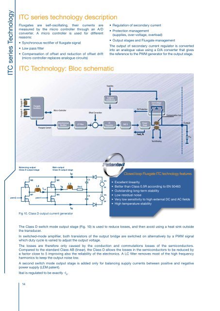
ITC Technology: Bloc schematic<br />
Fluxgate D'<br />
Fluxgate D<br />
Balancing output<br />
Class D output stage<br />
M8<br />
M7<br />
L4<br />
pwm1<br />
I bal<br />
Main output<br />
Class D output stage<br />
M6<br />
M5<br />
IN Fig 10. Class D output current generator<br />
14<br />
Fluxgate<br />
Oscillator<br />
Fluxgate Current<br />
Micro-Controller<br />
Synchronous<br />
Rectifier<br />
I S<br />
L3<br />
I P<br />
LP Filter<br />
Rm2<br />
C3<br />
C4<br />
Offset Correction<br />
+<br />
-<br />
+<br />
-<br />
+<br />
-<br />
V5<br />
24<br />
V6<br />
24<br />
• Regulation of secondary current<br />
• Protection management<br />
(supplies, over-voltage, overload)<br />
• Output stages and Fluxgate management<br />
The output of secondary current regulator is converted<br />
into an analogue value using a D/A converter that gives<br />
the reference to the PWM generator for the output stage.<br />
Supplies<br />
Supplies<br />
monitoring<br />
PI<br />
Regulator<br />
DAC 0<br />
OV Protection<br />
Fault_PS<br />
Power<br />
Stage<br />
Overvoltage<br />
Protection<br />
Test Winding<br />
Compensation Coil<br />
Output<br />
Closed loop Fluxgate ITC technology features<br />
• Excellent linearity<br />
• Better than Class 0.5R according to EN 50463<br />
• Outstanding long-term stability<br />
• Low residual noise<br />
• Very low sensitivity to high external DC and AC fields<br />
• High temperature stability<br />
The Class D switch mode output stage (Fig. 10) is used to reduce losses, and then avoid using a heat sink outside<br />
the transducer.<br />
In switched-mode amplifier, both transistors of the output bridge are switched on alternatively by a PWM signal<br />
which duty cycle is varied to adjust the output voltage.<br />
The losses are therefore only caused by the conduction and commutations losses of the semiconductors.<br />
Compared to the standard Class AB (linear), the Class D allows the losses in the semiconductors to be reduced by<br />
a factor close to 5 improving also the reliability of the electronics. A LC filter removes most of the high frequency<br />
harmonics to keep the output noise low.<br />
A second switch mode output stage is added only for balancing supply currents between positive and negative<br />
power supply (<strong>LEM</strong> patent).<br />
Ibal is regulated to be exactly -IS .<br />
R M