Variable-Voltage Class-E Power Amplifiers - EEMCS EPrints Service
Variable-Voltage Class-E Power Amplifiers - EEMCS EPrints Service
Variable-Voltage Class-E Power Amplifiers - EEMCS EPrints Service

Create successful ePaper yourself
Turn your PDF publications into a flip-book with our unique Google optimized e-Paper software.
<strong>Variable</strong>-<strong>Voltage</strong> <strong>Class</strong>-E <strong>Power</strong> <strong>Amplifiers</strong><br />
Mustafa Acar, Anne Johan Annema and Bram Nauta<br />
IC Design Chair, University of Twente, 7500 AE Enschede, The Netherlands<br />
Abstract— The <strong>Class</strong>-E power amplifier is widely used due<br />
to its high efficiency, resulting from switching at zero voltage<br />
and zero slope of the switch voltage. In this paper, we extend<br />
general analytical solutions for the <strong>Class</strong>-E power amplifier to the<br />
ideal single-ended <strong>Variable</strong>-<strong>Voltage</strong> <strong>Class</strong>-E (<strong>Class</strong>-EV V) power<br />
amplifier that switches at zero slope but not necessarily at zero<br />
voltage.<br />
The theory is verified by simulations and measurements, and<br />
show that the peak switch voltage of <strong>Class</strong>-EV V power amplifier<br />
is lower (up to ≈ 30% ) than in the conventional <strong>Class</strong>-E power<br />
amplifier; which can be utilized to obtain e.g. higher output<br />
power (up to ≈ 200% more) with lower power-added efficiency<br />
(maximum ≈ 20% less) from technologies with low-breakdown<br />
voltages.<br />
Index Terms— <strong>Power</strong> amplifiers, switching amplifiers.<br />
I. INTRODUCTION<br />
The <strong>Class</strong>-E power amplifier (PA) can achieve high efficiency<br />
due to its tuned load network that shapes the switch<br />
voltage to zero-voltage and zero-slope at the switch turnon<br />
moment. Many different aspects of the <strong>Class</strong>-E power<br />
amplifier (PA) have been extensively studied in the last three<br />
decades [1]- [7]. The reportedly ”sub-optimum operation” with<br />
nonzero-voltage or nonzero-slope switching [3] is hardly used<br />
because of its believed inferior performance.<br />
zero-slope switching<br />
<strong>Class</strong>-E [this paper]<br />
VV<br />
<strong>Class</strong>-E [3][5][7]<br />
zero-voltage switching<br />
<strong>Class</strong>-E [1][6]<br />
VS<br />
Fig. 1. Sub-optimum operation classes of <strong>Class</strong>-E PA<br />
In [1], zero-voltage and nonzero-slope switching operation<br />
only for RF-choke <strong>Class</strong>-E PAs has been investigated and it is<br />
found that these <strong>Class</strong>-E PAs have about 10% higher tolerance<br />
to switch (transistor) output capacitance than conventional RFchoke<br />
<strong>Class</strong>-E PAs. In [6], it has been shown that zero-voltage<br />
and nonzero-slope switching (denoted as variable-slope <strong>Class</strong>-<br />
E, <strong>Class</strong>-EVS (Fig.1)) operation of finite dc-feed inductance<br />
<strong>Class</strong>-E PAs allows using significantly larger switch (transistor)<br />
size (up to 110% more); which can be utilized in obtaining<br />
higher efficiency.<br />
To the best of the authors’ knowledge, analyses of nonzerovoltage<br />
and zero-slope switching <strong>Class</strong>-E PAs (denoted as<br />
<strong>Variable</strong>-<strong>Voltage</strong> <strong>Class</strong>-E, <strong>Class</strong>-EVV (Fig.1)) have not been<br />
presented in literature. This paper presents an analysis and<br />
some discussions on <strong>Class</strong>-EVV PAs to utilize their lower<br />
peak switch voltage feature to obtain higher output power with<br />
reasonably high power-added efficiency from transistor technologies<br />
with low-breakdown voltages. The analysis in this<br />
1-4244-0688-9/07/$20.00 ©2007 IEEE<br />
paper is based on closed form expressions like those presented<br />
in [5], [6] and [7] for <strong>Class</strong>-E PAs 1 . In the analysis, the finite<br />
dc-feed inductance (L), the switch (transistor) input/output<br />
capacitance (Cin/Cout) and on-resistance (Ron) (Fig. 2b) are<br />
all taken into account. As a result of the analysis, analytical design<br />
equations are presented showing the relation between the<br />
input parameters and the circuit component values. It is shown<br />
in this paper that <strong>Class</strong>-EVV can have up to ≈ 30% lower<br />
peak switch voltage than conventional <strong>Class</strong>-E PAs; which<br />
can be used to obtain up to ≈ 200% more output power with<br />
maximum ≈ 20% lower power-added efficiency 2 assuming the<br />
same transistor size, reliable peak voltage, matching network<br />
and pre-driver.<br />
v (t) /V<br />
1095<br />
C DD<br />
4<br />
3<br />
2<br />
1<br />
0<br />
P in<br />
2V DD,driver<br />
0<br />
R d<br />
V DD,driver<br />
Ld<br />
predriver<br />
L d Cin<br />
pre-driver<br />
G<br />
V V<br />
Con Coff<br />
���<br />
G<br />
D<br />
M<br />
I L<br />
L<br />
I S<br />
R ON<br />
D<br />
P switch<br />
V DD<br />
C<br />
V DD<br />
L<br />
C 0<br />
VC IC M<br />
C OUT<br />
���<br />
���<br />
���<br />
����<br />
time<br />
L 0<br />
tuned<br />
at � 0<br />
(a)<br />
C<br />
I R<br />
(b)<br />
S 0<br />
i (t) /I<br />
(c)<br />
R+jX<br />
C 0<br />
tuned at � 0<br />
3<br />
2.5<br />
2<br />
1.5<br />
1<br />
0.5<br />
0<br />
Lm Cm matching<br />
network<br />
L 0<br />
P match<br />
R+<br />
0 R m<br />
���<br />
���<br />
���<br />
R L<br />
matching<br />
network<br />
���<br />
Lm Cm P antenna<br />
R L<br />
����<br />
time<br />
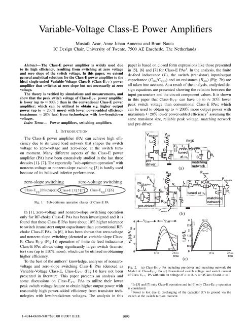
Fig. 2. (a) <strong>Class</strong>-EV V PA including pre-driver and matching network (b)<br />
Model of <strong>Class</strong>-EV V PA (c) Normalized switch voltage and switch current<br />
of <strong>Class</strong>-EV V PA with turn-on voltage of α =2, α =0(<strong>Class</strong>-E) and α =1<br />
1In [5] and [7] only <strong>Class</strong>-E operation and in [6] only <strong>Class</strong>-EV S operation<br />
is considered.<br />
2<strong>Power</strong> is lost due to discharging of the capacitor (C) to ground via the<br />
switch at the switch turn-on moment.
II. ANALYSIS OF CLASS-EVV POWER AMPLIFIER<br />
A single ended switching PA topology and its model are given<br />
in Fig.2a and Fig.2b respectively. An analytical solution for<br />
the model in Fig.2b to operate as a <strong>Class</strong>-E PA (e.g. switching<br />
at zero-voltage and zero-slope) is given in [5] and [7] 3 .In<br />
[6], switching with variable slope aspect was generalized<br />
and analytical design equations for <strong>Class</strong>-EVS (e.g. switching<br />
at zero-voltage and variable-slope) is given. In the current<br />
paper, the variable voltage aspect is generalized and general<br />
analytical solution for <strong>Class</strong>-EVV (e.g. switching at variablevoltage<br />
and zero-slope) is given based on the model in Fig. 2b.<br />
If the correct input parameters and circuit element values are<br />
chosen, the circuit in Fig. 2a properly operates as a <strong>Class</strong>-EVV<br />
PA by satisfying the following conditions (1):<br />
vC(2π/ω) =αVDD and<br />
dvC(t)<br />
dt<br />
�<br />
�<br />
�<br />
� t=2π/ω<br />
=0 (1)<br />
where αVDD is the voltage of vC(t) at the moment the switch<br />
is closed; for conventional <strong>Class</strong>-E operation α =0. However,<br />
in <strong>Class</strong>-EVV operation α is a real value 4 that can be selected<br />
freely and therefore gives a degree of freedom in the design of<br />
a <strong>Class</strong>-EVV PA. A design set K = {KL,KC,KP ,KX,KR}<br />
(Table 1) can be derived that relates circuit element values<br />
and operating conditions such as supply voltage, operating<br />
frequency and output power for the switching PA in Fig.2a.<br />
In this section, closed form analytical expressions for each<br />
element of the <strong>Class</strong>-EVV are derived; which enables infinitely<br />
many <strong>Class</strong>-EVV realizations, to be selected by the parameters<br />
q =1/(ω √ LC), m = ωRonC ( [5], [6], [7]) and α. The<br />
design parameters q and m are free variables like α and<br />
mathematically can be assigned any positive real value 5 .<br />
Table 1: Design Set K for <strong>Class</strong>-EVV PA 6<br />
KL = ωL<br />
R ,KC = ωCR,KP =<br />
POUT R<br />
V 2 ,KX =<br />
DD<br />
X<br />
R , KR = Ron<br />
R<br />
This section presents the derivation of the design set K for<br />
<strong>Class</strong>-EVV PAs.<br />
A. Circuit Description and Assumptions<br />
The circuit model of the <strong>Class</strong>-E PA is given in Fig.2b. For<br />
the analysis and the derivations in this paper a number of<br />
assumptions are made:<br />
• the only real power loss occurs on RL, Ron, Rd, R0 and<br />
Rm.<br />
• The capacitors Cin and Cout are assumed to be linear.<br />
• the switch (transistor) operates instantly with onresistance<br />
(Ron) and infinite off-resistance<br />
3 Note that the analysis in [5] is extended in [7] by taking into account a<br />
non-zero switch on-resistance.<br />
4 Theoretically, α
By using the continuity of the inductor current and the ca- D. Efficiency and Output <strong>Power</strong> of <strong>Class</strong>-EVV<br />
pacitor voltage at the switch turn-off moment two independent<br />
equations follow that have the same format:<br />
Taking the three loss mechanisms (Pin, Pswitch, Pmatch)<br />
shown in Fig. 2 and the existence of certain switch (transistor)<br />
fi(p, q, ϕ, m, α) = pai(q, m, α)cos(ϕ)+pbi(q, m, α)sin(ϕ)<br />
breakdown-voltage<br />
+ci(q, m, α) =0, where i =1, 2.<br />
The variables p and ϕ can be solved by using f1(p, q, ϕ, m, α)<br />
and f2(p, q, ϕ, m, α) in terms of q, m and α as given in<br />
the appendix. Here, q, m and α are free variables that can<br />
mathematically take any positive real value.<br />
7 (VBD = z(q, m, α) · VDD) into account<br />
the efficiency and the power on the antenna can be expressed:<br />
Drain Efficiency(η): derived as a function of q, m and α.<br />
η(q, m, α) =1− Pswitch<br />
� π<br />
w<br />
0 =1−<br />
VDDI0<br />
vCon (t)2dt � π<br />
ω<br />
VDD vCon (t)dt<br />
0<br />
<strong>Power</strong>-Added Efficiency(PAE): as a function of q, m and<br />
α.<br />
C. Design sets for <strong>Class</strong>-EVV operation<br />
The results of the mathematical derivation of the solutions<br />
leading to <strong>Class</strong>-EVV operation can be used to derive an easyto-use<br />
design procedure for <strong>Class</strong>-EVV PAs. Using the result<br />
of the derivation for p(q, m, α) and ϕ(q, m, α), analytical<br />
expressions for the design set K = {KL,KC,KP ,KX,KR}<br />
can readily be derived.<br />
KL : follows from the principle of power conservation:<br />
I 2 RR/2+Pswitch = I0VDD<br />
In this relation, I0 is the average supply current:<br />
(8)<br />
I0 = ω<br />
� π/ω<br />
vCon (t)dt<br />
2πRon<br />
(9)<br />
0<br />
and Pswitch is the power spent on Ron:<br />
� π<br />
w<br />
Pswitch = ω<br />
vCon<br />
2πRon 0<br />
(t)2dt Substitution of (9) and p in (8) yields<br />
−(pVDDq)<br />
KL(q, m, α) =<br />
2mπ � π<br />
w ω 0 (vCon (t)2 − VDDvCon (t))dt<br />
Since p and ϕ are all functions of q, m and α, KL is a function<br />
of only q, m and α.<br />
KC: follows directly from the definition of q and KL:<br />
KC(q, m, α) = 1/(q2KL(q, m, α))<br />
KP : can easily be found as a function of q, m and α by using<br />
IR = � 2POUT /R and the definition of p:<br />
KP (q, m, α) =p(q, m, α) 2 /(2KL(q, m, α) 2 )<br />
KX: can be derived using two fundamental quadrature<br />
Fourier components of vC(t).<br />
vR =<br />
vX =<br />
� π<br />
ω<br />
0<br />
� π<br />
ω<br />
0<br />
vCon (t)<br />
π<br />
vCon (t)<br />
π<br />
sin(ωt+ϕ) dt+<br />
� 2π<br />
ω<br />
π<br />
ω<br />
� 2π<br />
ω<br />
cos(ωt+ϕ) dt+<br />
π<br />
ω<br />
vCoff (t)<br />
sin(ωt+ϕ) dt<br />
π<br />
vCoff (t)<br />
cos(ωt+ϕ) dt<br />
π<br />
KX(q, m, α) =vX/vR<br />
KR: follows from the definition of m and KC:<br />
KR(q, m, α) =KC(q, m, α)/m<br />
1097<br />
PAE(q, m, α) = Pantenna − Pin<br />
VDDI0 ⎛<br />
= η(q, m, α) ⎝<br />
1<br />
1+ √ n−1+QL<br />
Qm<br />
− c1c2<br />
2d 2 Qd<br />
⎞<br />
KC(q, m, α)<br />
⎠<br />
KP (q, m, α)<br />
where, Pantenna = POUT − Pmatch, n = RL<br />
R , Pin ≈<br />
ωCinV 2 DDdriver /(2Qd), c1 = Cin/Cout, c2 = Cout/C, d =<br />
VDD/VDDdriver . Qm is the quality factor of the inductors Lm<br />
and L0. Qd is the quality factor of Ld (Fig. 2b).<br />
<strong>Power</strong> on Antenna(Pantenna): as a function of q, m and α.<br />
Pantenna(q, m, α) = KP (q, m, α)<br />
z(q, m, α) 2<br />
n<br />
1+ √ n−1+QL<br />
Qm<br />
V 2 BD<br />
RL<br />
Fig. 3. PAE and Pantenna using technology and design parameters in [4]<br />
The value of c1, d and VBD depend on the characteristics of<br />
the transistor technology. For a certain operation frequency<br />
and transistor technology, m only depends on the value of<br />
c2 since m = ωβ/c2 where β = RonCout which depends<br />
on the transistor technology. Therefore, for a given transistor<br />
technology, impedance transformation ratio (n), Qm and Qd,<br />
PAE and Pantenna both are a function of only q, m and<br />
α. InFig.3,PAE and Pantenna are plotted as a function<br />
of α for a few values of q using the design and technology<br />
parameters in [4]. In [4] 8 , QL =3, Qd =3, n =3, c2 =1,<br />
ω =2π · 1.7 · 10 9 rad/sec and the transistor technology is<br />
0.13um CMOS (thick oxide) for which VBD ≈ 2.5 · 3.56 V 9 ,<br />
c1 ≈ 4 and RonCout ≈ 10 −12 ; resulting in m ≈ 0.011.<br />
7 Here VBD refers to gate-drain oxide breakdown voltage which is assumed<br />
to be lower than junction breakdown voltages. It is also assumed that<br />
VDD driver is chosen as max. reliable gate-source oxide breakdown voltage.<br />
8 Value of q is calculated as 1.2 from the circuit element values in [4] and<br />
Qm for Lm and L0 (bondwire) is assumed to be 30.<br />
9 In [4], breakdown voltage is doubled by using a cascode topology.
In [4], an optimization procedure based upon approximations<br />
and simulation results is given for <strong>Class</strong>-E PAs. The PAE<br />
measurement results given in [4] (67%, for conventional <strong>Class</strong>-<br />
E PA) is close to theoretical value given in Fig.3 (≈ 71%). The<br />
difference can be attributed to the losses due to ground bonding<br />
and dc-feed inductance; which are not taken into account in<br />
the analytical design equations in this paper.<br />
Fig. 3 shows the strong dependence of PAE and Pantenna<br />
both on q and α. It can be seen in Fig. 3 that the maximum<br />
Pantenna for <strong>Class</strong>-EVV (q =0.6,α=2)is1.65 times higher<br />
than the maximum Pantenna for conventional <strong>Class</strong>-E PA (q =<br />
1.2,α =0). Besides, for q =0.6 <strong>Class</strong>-EVV (α =1) can<br />
have ≈ 80% more Pantenna with only 3% less PAE than<br />
conventional <strong>Class</strong>-E PA (α = 0). For the same q = 0.6,<br />
<strong>Class</strong>-EVV (α =2) can have ≈ 200% more Pantenna with<br />
≈ 16% less PAE than the conventional <strong>Class</strong>-E PA (α =0).<br />
2<br />
1<br />
1<br />
2<br />
v C (t)<br />
v RL (t)<br />
��� ���<br />
v RL (t)<br />
���<br />
1<br />
v RL (t)<br />
v C (t) v C (t)<br />
Fig. 4. Measurement Results for α =0, 1 and 2<br />
III. PROOF OF CONCEPT DESIGN<br />
We verified the given design equations in this paper by<br />
simulating the model in Fig.2b by transient and pss (periodic<br />
steady state) simulations in Spectre (Cadence). Very good<br />
agreement in the waveforms is observed between the simulations<br />
and the theory with a discrepancy of ≈ 3%; attributed<br />
to the finite value of QL =5used in the simulations.<br />
Measurement results at low frequency (5MHz) are given in<br />
Table 2 and Fig. 4; which verify that <strong>Class</strong>-EVV can have<br />
higher output power with reasonable efficiency in comparison<br />
to conventional <strong>Class</strong>-E. The three PAs in Table 2 are<br />
implemented on pcb by using discrete transistor (start499)<br />
with maximum allowed peak voltage (vC ≈ 4.5 V), ceramic<br />
capacitors and air-core inductors. In the measurements, a<br />
54642A Oscilloscope, 34401A DMV and a E3631A DC power<br />
supply are used. The switch (transistor) of the <strong>Class</strong>-E PA is<br />
directly driven with a square signal from an Agilent 33250A<br />
signal source. Due to lack of the RF source at low frequency<br />
Pdrive couldn’t be measured but is calculated to be ≈ 3 mW.<br />
2<br />
1098<br />
Table 2: Measurement Results and Design Details<br />
Design Details <strong>Class</strong>-E <strong>Class</strong>-EV Vα=1 <strong>Class</strong>-EV Vα=2<br />
(q,α,m,QL,n) (0,0,0.001,5,2.3) (0,1,0.001,5,2.3) (0,2,0.001,5,2.3)<br />
Frequency, VDD 5 MHz, 1.4 V 5 MHz, 1.6 V 5 MHz, 1.9 V<br />
POUT ,PDC 19.9, 29.4 mW 30.4, 48.4 mW 55.2, 108.3 mW<br />
R, η 22Ω, 67.7% 22Ω, 62.8% 22Ω, 51.0%<br />
Lm, L,Vpeak 1.6, 12 uH, 4.2 V 1.4, 12 uH, 4.2 V 1.3, 12 uH, 4.2 V<br />
C, Cm 0.26, 0.72 nF 0.42, 0.72 nF 0.79, 0.72 nF<br />
IV. CONCLUSION<br />
This paper shows the analytical design equations, and the<br />
time domain analytical solution for <strong>Class</strong>-EVV PAs, including<br />
finite dc-feed inductance and switch input/output capacitance<br />
and on-resistance. In comparison to conventional <strong>Class</strong>-E<br />
PAs, <strong>Class</strong>-EVV PAs can have lower peak switch voltage;<br />
which can be utilized to obtain high output power using lowvoltage<br />
transistor technologies (e.g. CMOS). This paper shows<br />
(theoretically and experimentally) that <strong>Class</strong>-EVV PAs can<br />
have up to ≈ 200% more output power than conventional<br />
<strong>Class</strong>-E PAs under the same drive, load and reliable peak<br />
voltage conditions, with only a modest PAE penalty.<br />
REFERENCES<br />
[1] T. Suetsugu, M.K. Kazimierczuk, ”Analysis of Sub-Optimum Operation<br />
of <strong>Class</strong> E Amplifier” Circuits and Systems, Proceedings of the 46th IEEE<br />
International Midwest Symposium, vol. 3, pp: 1071- 1074, Dec. 2003.<br />
[2] D.Y.C. Lie, et al ”The limitations in applying analytic design equations<br />
for optimal class E RF power amplifiers design” VLSI Design, Automation<br />
and Test, IEEE 2005, pp:161 - 164<br />
[3] F.H. Raab, ”Idealized Operation of The class E <strong>Power</strong> Amplifier,” IEEE<br />
Trans. Circuit. Syst., vol. 24. no. 12, Dec. 1977.<br />
[4] Mazzanti, A,et al ”Analysis of reliability and power efficiency in cascode<br />
class-E PAs,” IEEE, JSSC, May 2006, vol.24, pp:1222 - 1229.<br />
[5] M. Acar, A.J. Annema, B. Nauta ”Generalized Design Equations for<br />
<strong>Class</strong>-E <strong>Power</strong> <strong>Amplifiers</strong> with Finite DC Feed Inductance” 36th European<br />
Microwave Conference, September 2006, pp. 13081311.<br />
[6] M. Acar, A.J. Annema, B. Nauta ”Generalized Analytical Design Equations<br />
for <strong>Variable</strong> Slope <strong>Class</strong>-E <strong>Power</strong> <strong>Amplifiers</strong>” 13th IEEE International<br />
Conference on Electronics, Circuits and Systems, December 2006.<br />
[7] M. Acar, A.J. Annema, B. Nauta ”Analytical Design Equations for <strong>Class</strong>-<br />
E <strong>Power</strong> <strong>Amplifiers</strong> with Finite DC Feed Inductance and Switch On<br />
Resistance” IEEE, International Symposium on Circuits and Systems,<br />
May 2007 (accepted).<br />
APPENDIX I<br />
p and ϕ are expressed in terms of q, m and α as follows: