CIKC Brochure 201003_5b - University of Cambridge
CIKC Brochure 201003_5b - University of Cambridge
CIKC Brochure 201003_5b - University of Cambridge

You also want an ePaper? Increase the reach of your titles
YUMPU automatically turns print PDFs into web optimized ePapers that Google loves.
Contents:<br />
2<br />
Technology<br />
Projects<br />
9<br />
Facilities<br />
11<br />
Training<br />
13<br />
Commercialisation<br />
15<br />
Small Grants<br />
16<br />
Work with <strong>CIKC</strong><br />
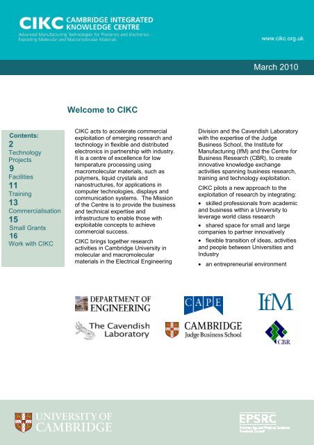
Welcome to <strong>CIKC</strong><br />
<strong>CIKC</strong> acts to accelerate commercial<br />
exploitation <strong>of</strong> emerging research and<br />
technology in flexible and distributed<br />
electronics in partnership with industry.<br />
It is a centre <strong>of</strong> excellence for low<br />
temperature processing using<br />
macromolecular materials, such as<br />
polymers, liquid crystals and<br />
nanostructures, for applications in<br />
computer technologies, displays and<br />
communication systems. The Mission<br />
<strong>of</strong> the Centre is to provide the business<br />
and technical expertise and<br />
infrastructure to enable those with<br />
exploitable concepts to achieve<br />
commercial success.<br />
<strong>CIKC</strong> brings together research<br />
activities in <strong>Cambridge</strong> <strong>University</strong> in<br />
molecular and macromolecular<br />
materials in the Electrical Engineering<br />
www.cikc.org.uk<br />
March 2010<br />
Division and the Cavendish Laboratory<br />
with the expertise <strong>of</strong> the Judge<br />
Business School, the Institute for<br />
Manufacturing (IfM) and the Centre for<br />
Business Research (CBR), to create<br />
innovative knowledge exchange<br />
activities spanning business research,<br />
training and technology exploitation.<br />
<strong>CIKC</strong> pilots a new approach to the<br />
exploitation <strong>of</strong> research by integrating:<br />
• skilled pr<strong>of</strong>essionals from academic<br />
and business within a <strong>University</strong> to<br />
leverage world class research<br />
• shared space for small and large<br />
companies to partner innovatively<br />
• flexible transition <strong>of</strong> ideas, activities<br />
and people between Universities and<br />
Industry<br />
• an entrepreneurial environment
<strong>CIKC</strong><br />
Technology<br />
2<br />
<strong>CIKC</strong> has three core technology themes:<br />
– Plastic (opto-) electronics: flexible<br />
displays/electronics and distributed<br />
electronics on rigid substrates at a “low”<br />
temperature budget<br />
– Augmented or additive processing on<br />
active substrates (e.g. liquid crystal on<br />
silicon devices, LCOS)<br />
– Complementary actions such as<br />
photovoltaic or energy storage/batteries<br />
Molecular and macromolecular material<br />
based components are likely to meet a very<br />
large range <strong>of</strong> commercial applications in<br />
displays, lighting, photovoltaics, smart<br />
packaging, smart windows, RFID etc. For<br />
example, solution-based processing <strong>of</strong><br />
polymer semiconductors <strong>of</strong>fers the potential<br />
<strong>of</strong> integrating electronic, optical and photonic<br />
devices into flexible, low-cost plastic<br />
substrates enabling a range <strong>of</strong> innovative<br />
products, and LCOS devices are becoming<br />
the main contenders in the microdisplays<br />
industry.<br />
Technology Portfolio<br />
Project Topic Partners<br />
3PV,<br />
3PV+<br />
OPV Carbon Trust,<br />
TTP<br />
Process technology for roll-to-roll printing <strong>of</strong> organic<br />
photovoltaics on flexible substrates<br />
HiPZOT TCO, i-TFTs CAPE, Plasma<br />
Quest<br />
Low temperature deposition <strong>of</strong> transparent conductors<br />
and inorganic TFTs based on zinc oxide on flexible<br />
substrates<br />
PASSBACK LCOS CAPE<br />
Liquid crystal on silicon (LCOS) devices for phase-only<br />
holography for applications in video projection and<br />
telecommunications<br />
PIES,<br />
PSIAC<br />
Optical datacoms Dow Corning,<br />
Avago<br />
Low cost polymer waveguide interconnects for optical<br />
communications<br />
PLACORD, LEAF Reflective Display Advex, Dow<br />
Corning<br />
Lamination processes for electroactive materials on<br />
flexible foils, e.g. large area liquid crystal reflective<br />
displays<br />
MIPE,<br />
PRIME,<br />
COPE<br />
oTFT Plastic Logic,<br />
Merck, DuPont<br />
Teijin Films<br />
Scalable self-aligned printing processes for next<br />
generation polymer TFT circuits<br />
ROOT oTFT Hitachi<br />
Characterisation techniques to understand operational<br />
degradation in organic TFTs<br />
ACET<br />
Roadmaps for MMM technology.
Printing for Manufacturing <strong>of</strong> Electronics (PRIME)<br />
www.cikc.org.uk<br />
A self-aligned method for producing fully-downscaled printed organic FETs has been developed<br />
and this project aims to develop this as a manufacturable process for organic transistor circuit<br />
fabrication.<br />
Partners: Plastic Logic, DuPont Teijin Films, Merck<br />
Technical objectives<br />
• Prove manufacturability <strong>of</strong> printing process<br />
• Assess and improve manufacturing yield and uniformity<br />
• Assess device reliability<br />
• Development <strong>of</strong> prototype<br />
Achievements<br />
-<br />
+<br />
• Reliable fabrication <strong>of</strong> arrays <strong>of</strong> SAP electrodes with channel length <strong>of</strong> 200-400 nm and<br />
100% yield<br />
• Fabrication <strong>of</strong> all-printed, short-channel organic FETs with gold and silver electrodes to<br />
reduce series and contact resistance<br />
1 Self-aligned printing (SAP)<br />
2 SAM<br />
F F F F<br />
F F F<br />
F F<br />
SH<br />
SH<br />
CN<br />
SH<br />
Au<br />
H H H H<br />
H H H<br />
H H<br />
SH SH SH<br />
Y.-Y. Noh, et al., Nature Nano, (2007).<br />
ga<br />
3 High mobility organic<br />
semiconductors<br />
Source<br />
Source<br />
Gate<br />
Drain<br />
100 µm<br />
Channel<br />
Ink jet<br />
printed<br />
TFT<br />
5 Self-aligned gate architecture (SAG)<br />
SAG<br />
dielectric<br />
Drain<br />
4 Thin gate dielectrics<br />
3
<strong>CIKC</strong><br />
High Performance Zinc Oxide Thin Film Transistors (HiPZOT)<br />
Plasma Quest Ltd has developed a novel system for sputtering thin films at high deposition rates<br />
with exceptional control <strong>of</strong> material properties and low substrate temperatures. This project aims<br />
to fabricate high mobility thin film transistors based on zinc oxide on plastic substrates using the<br />
Plasma Quest HiTUS system, for applications such as active matrix backplanes for OLED displays.<br />
As well as being compatible with plastic substrates, zinc oxide technology potentially <strong>of</strong>fers lower<br />
cost and higher performance than amorphous silicon.<br />
Partner: Plasma Quest Ltd.<br />
Results<br />
4<br />
• Fabrication <strong>of</strong> a new generation <strong>of</strong> TFTs using metal oxide based materials is possible at<br />
plastic-compatible temperatures. Mobility µFE 10 cm 2 V -1 s -1 and switching ratio >10 6<br />
achieved with an amorphous indium zinc oxide (IZO) channel.<br />
• Hafnium oxide dielectric with amorphous structure, resistivity > 10 14 Ωcm and εr = 30.<br />
• Aluminium oxide dielectric with resistivity > 10 14 Ωcm.<br />
• HiTUS sputtering <strong>of</strong>fers clear advantages for material control over rf magnetron sputtering.<br />
• Excellent optical properties observed in all films - fully transparent devices possible.<br />
V GS = -2.5 V<br />
V GS = 0.0 V<br />
V GS = 2.5 V<br />
V GS = 5.0 V<br />
V GS = 7.5 V<br />
V GS = 10.0 V<br />
TDP00C_a<br />
-5 0 5 10 15 20 25 30<br />
V [V] DS<br />
IZO TFT Characteristics<br />
0.6<br />
0.5<br />
0.4<br />
0.3<br />
0.2<br />
0.1<br />
0.0<br />
-0.1<br />
I DS [mA]<br />
Transparent metal oxide TFTs<br />
Amorphous Indium Zinc Oxide
Polymer Interconnects with Environmental Stability (PIES)<br />
www.cikc.org.uk<br />
This project aims to determine how polymer waveguides able to operate in environmentally hostile<br />
applications can be fabricated using high resolution imprinting techniques in a low cost manner and<br />
to produce a range <strong>of</strong> optically functional multimode components suitable for direct integration with<br />
electrical circuit boards.<br />
Partners: Dow Corning, Tyco, WCPC, Avago<br />
Successful integration <strong>of</strong> optical components into existing electronics architectures and<br />
manufacturing processes requires material capable <strong>of</strong> withstanding high-temperatures related to<br />
soldering and lamination. Siloxane polymers from Dow Corning can withstand > 250°C, can be<br />
integrated onto standard FR4 PCB and have low intrinsic optical loss.<br />
This project is an investigation into low cost, high performance optical integration components<br />
using these siloxane polymers. The aim is to take the technology to the stage where it can be<br />
readily transferred to production and to enable a wide range <strong>of</strong> low cost products based on optohybrids.<br />
Polymer waveguides over copper tracks<br />
10 cm<br />
Polymer waveguide<br />
over copper tracks<br />
10 card optical<br />
backplane<br />
10 card optical<br />
backplane<br />
Optical transceiver integrates optical waveguide and<br />
electronic components on a common PCB substrate<br />
with novel through-board connectors for endfire coupling<br />
5
<strong>CIKC</strong><br />
6<br />
Plastic Large Area Colour Reflective Displays (PLACORD)<br />
New Smectic A liquid crystal materials and electro-optic technology for reflective colour and<br />
‘electronic print’ displays have been developed and this project is developing processes to<br />
laminate these materials between plastic substrates for large area display applications.<br />
Partners: Dow Corning, Advex<br />
Advantages <strong>of</strong> Smectic A liquid crystal for reflective displays<br />
• Bistable – low power consumption<br />
• Greyscale response.<br />
• Bright white state > 55% reflectivity.<br />
• Reflective contrast > 7:1<br />
• Stackable for full colour displays<br />
• Very large arrays <strong>of</strong> pixels can be multiplexed<br />
Project Aims:<br />
− Set up a state-<strong>of</strong>-the-art laboratory for making plastic encapsulated devices.<br />
− To develop and test liquid crystal guest-host materials for e-posters.<br />
− To make a composite tile involving three stacked layers <strong>of</strong> single colour sub-tiles.<br />
Stable with no<br />
voltage applied.<br />
Electro-optic bistability in Smectic-A liquid crystal<br />
Clear<br />
State LC<br />
Schematic <strong>of</strong> SmA liquid crystals<br />
AC voltage low frequency (~50<br />
AC voltage high frequency (1–2 kHz)<br />
Schematic <strong>of</strong> state changing conditions<br />
Scattered<br />
State LC<br />
Stable with no<br />
voltage applied.
Printed Polymer Photovoltaics (3PV)<br />
www.cikc.org.uk<br />
Objective: 2-year project to develop roll-to-roll manufacturing processes for printed polymer solar<br />
cells<br />
Partner: Carbon Trust Advanced Photovoltaics Research Accelerator<br />
Technology Approach: Polymer-based photovoltaics are improving in efficiency to levels where<br />
large-area applications are attractive. Roll-to-roll fabrication by printing will allow major cost<br />
reductions compared with incumbent silicon technology.<br />
Technical objectives<br />
• Develop printing processes for thin active layer deposition<br />
• Develop new anode materials<br />
• Understand effect <strong>of</strong> printing process on polymer nanostructure<br />
Commercialisation<br />
- Carbon Trust will provide up to £5m funding, initially as a research grant (matching funding for<br />
3PV), and then as equity investment in a new start-up.<br />
- Aim to launch spinout in 2010, with combination <strong>of</strong> strategic investor and seed investor funding<br />
to match Carbon Trust contribution.<br />
Roll-to-roll printing<br />
Printed modules<br />
Printed films<br />
7
<strong>CIKC</strong><br />
8<br />
Photonic and Sensing Systems based on CMOS Backplanes (PASSBACK)<br />
This project aims to develop high quality prototype phase only liquid crystal on silicon (LCOS)<br />
devices for applications including holographic projection systems and telecommunications<br />
modules. The project is establishing equipment and processes for a wide range <strong>of</strong> additive<br />
processing based on the Silicon CMOS platform including opto-hybrids and devices.<br />
Aim:<br />
Progress:<br />
An ideal phase<br />
hologram can<br />
manipulate light<br />
beams without<br />
loss <strong>of</strong> photons.<br />
• To develop in-house LCOS prototype device fabrication processes for high-spec<br />
LCOS devices<br />
• To build prototype devices for various applications<br />
• Successfully commissioned a 20 step semi-automatic LCOS prototyping process<br />
• Phase-only holographic projection engine prototype built and tested in collaboration<br />
with commercial partner, ALPS<br />
Applications <strong>of</strong> phase-only<br />
LCOS technology<br />
Built environment<br />
Holographic<br />
μ-projector<br />
Telecoms<br />
Lab-on-a-chip<br />
3D
Infrastructure and facilities<br />
<strong>CIKC</strong> has a collectively owned core <strong>of</strong> capital<br />
equipment to enable product development<br />
right through to pilot production. <strong>CIKC</strong><br />
collaborative projects draw upon both<br />
physical and personnel resource across the<br />
partnership.<br />
The CAPE laboratories and the Cavendish<br />
are well-equipped with dark-room, wet labs,<br />
communications demonstration and test<br />
equipment, general electronic component<br />
assembly and test as well as large very high<br />
quality clean-room suites, which are utilised<br />
by <strong>CIKC</strong> projects.<br />
Suss Kadett Semi- Automatic Device<br />
Bonder allows accurate assembly for<br />
LCOS fabrication.<br />
Plasma Quest HiTUS sputter system for<br />
deposition <strong>of</strong> a wide range <strong>of</strong> transparent<br />
conducting oxides on plastic substrates for<br />
flexible electronics.<br />
www.cikc.org.uk<br />
<strong>CIKC</strong> has installed equipment sets for<br />
www.<br />
1. Liquid Crystal on Silicon (LCOS) device<br />
prototyping<br />
2. Printing <strong>of</strong> organic electronic devices<br />
3. Low temperature deposition <strong>of</strong><br />
transparent conducting oxides on plastic<br />
substrates.<br />
4. Lamination <strong>of</strong> large area liquid crystal<br />
displays on plastic<br />
We welcome enquiries from industry and<br />
other academic institutions interested in<br />
accessing this infrastructure.<br />
Litrex L120L industrial multi-nozzle ink jet<br />
System for process development for<br />
organic electronic circuits. The tool is<br />
currently setup for ink jet printing <strong>of</strong> gold<br />
and silver nanoparticle inks.<br />
Bench top coater/laminators for liquid<br />
crystals on plastic substrates for plastic<br />
display structures, plastic electronics<br />
and plastic based photovoltaics.<br />
9
<strong>CIKC</strong><br />
10<br />
Roadmapping<br />
Successful achievement <strong>of</strong> <strong>CIKC</strong> goals<br />
requires a high level <strong>of</strong> collaboration and<br />
integration across the various programme<br />
themes, projects and activities. This is<br />
particularly challenging given the complexity<br />
<strong>of</strong> both the underlying science/technology<br />
and the potential routes to commercial<br />
exploitation, together with the diversity and<br />
number <strong>of</strong> stakeholders and projects<br />
involved.<br />
Roadmapping is being used as a framework<br />
to support strategic planning for individual<br />
projects within <strong>CIKC</strong>, as well as supporting<br />
alignment within the programme.<br />
Roadmapping techniques are widely used in<br />
industry to explore, manage and<br />
communicate the linkages between<br />
technology and research investments,<br />
product developments, business objectives<br />
and market opportunities, using a structured<br />
visual framework.<br />
The exploratory roadmapping method<br />
provides a structured means for mapping and<br />
exploring <strong>CIKC</strong> project exploitation<br />
opportunities, in order to<br />
• Support project strategy development<br />
at an early stage.<br />
• Clarify exploitation paths (in particular,<br />
to identify application opportunities in<br />
the short, medium and long term).<br />
• Identify issues <strong>of</strong> relevance to other<br />
projects to support programme<br />
alignment<br />
• Initiate roadmapping in projects.<br />
Exploratory workshops have been held for a<br />
number <strong>of</strong> <strong>CIKC</strong> projects using a<br />
roadmapping template to capture participant<br />
views and guide discussion. The summary<br />
view is then used to create outline roadmaps<br />
which highlight short, medium and long-term<br />
application opportunities and associated<br />
exploitation enablers and barriers.<br />
From a programme alignment perspective,<br />
the key outcome from each workshop is a<br />
report summarising the commercial and<br />
exploitation issues identified, including short,<br />
medium and long term application<br />
opportunities, in a format that non-technical<br />
experts can understand and which are <strong>of</strong><br />
relevance to the commercialisation projects.
Business & training<br />
Training Courses<br />
The educational and training component<br />
provides <strong>CIKC</strong>-funded staff and students with<br />
skills and tools to understand the challenges<br />
and opportunities in the application <strong>of</strong> science<br />
and technology to the marketplace.<br />
Executive Education<br />
<strong>CIKC</strong> can facilitate the attendance <strong>of</strong> staff<br />
from our industrial partners on the Open<br />
Programme <strong>of</strong> Executive Education at the<br />
Judge Business School and executive<br />
training courses run by the Institute for<br />
Manufacturing.<br />
The <strong>Cambridge</strong> Executive Education<br />
programme is a portfolio <strong>of</strong> over 20 courses<br />
enabling participants to extend their skills and<br />
understanding to achieve personal<br />
development and career objectives. Most<br />
programmes are <strong>of</strong>fered in a 2-day format at<br />
<strong>Cambridge</strong> <strong>University</strong>. More details are<br />
www.cikc.org.uk<br />
available at www.jbs.cam.ac.uk/execed/<br />
Many <strong>of</strong> the IfM's courses are run on an incompany<br />
basis with modules tailored to<br />
address the issues facing a particular<br />
organisation and typically involve a<br />
combination <strong>of</strong> technical, management and<br />
s<strong>of</strong>tware training. For details see:<br />
http://www.ifm.eng.cam.ac.uk/<br />
Representatives from <strong>CIKC</strong> partner<br />
companies who would like to discuss what<br />
assistance <strong>CIKC</strong> can <strong>of</strong>fer your company<br />
please contact the <strong>CIKC</strong> <strong>of</strong>fice.<br />
Ignite<br />
<strong>CIKC</strong> sponsors students and researchers to<br />
attend this intense, one-week training<br />
programme for aspiring entrepreneurs and<br />
corporate innovators which has been run by<br />
The Centre for Entrepreneurial Learning<br />
(CfEL) since 1999. The 2010 course will run<br />
from June 27-July 3:<br />
http://www.cfel.jbs.cam.ac.uk/programmes/ignite/<br />
MOTI<br />
Management <strong>of</strong> Technology and Innovation<br />
equips students with an understanding <strong>of</strong><br />
how their science, engineering and<br />
technology knowledge can be transformed<br />
into commercial products and services, and<br />
the pathways by which innovations reach the<br />
market place. Lectures take place in the<br />
evenings during Michaelmas and Lent terms.<br />
Ignite attendee feedback:<br />
“Ignite not only provides me with the knowledge about entrepreneurship but also provides me with a<br />
valuable network, both which I believe are very important to my future development.”<br />
“After Ignite, my business idea has a brighter future.”<br />
“From the course, I have gained all the tools required to build a successful business.”<br />
11
<strong>CIKC</strong><br />
12<br />
Technology and Innovation Management<br />
This three-day course helps managers to<br />
understand the key tools and techniques<br />
needed to exploit technological investments<br />
and opportunities. Attendees gain a working<br />
knowledge <strong>of</strong> how to:<br />
• integrate technological considerations into<br />
business strategy and planning processes<br />
• understand and communicate the value <strong>of</strong><br />
technology investments<br />
• manage new product development in the<br />
context <strong>of</strong> the innovation system<br />
• use appropriate, process-based<br />
technology management approaches<br />
Further details <strong>of</strong> the course are available<br />
from http://www.ifm.eng.cam.ac.uk<br />
ISMM Module<br />
This module is on <strong>of</strong>fer to <strong>CIKC</strong> postgraduate<br />
students or research staff. The two-week<br />
course runs in January 2011 at IfM. At the<br />
end <strong>of</strong> the module, students will have a<br />
practical Technology and Innovation<br />
Management toolkit which they will be able to<br />
apply to technology commercialisation<br />
activities.<br />
i-Teams<br />
This is an opportunity for<br />
entrepreneurial post-graduate<br />
students to build go-to-market<br />
strategies for real inventions.<br />
Each i-Team, consisting <strong>of</strong> 7 students from<br />
different disciplines, assesses the<br />
commercial prospects for a <strong>University</strong><br />
technology by talking to target customers and<br />
defines directions for future technology<br />
development. For more information see<br />
www.iteamsonline.org.<br />
Student projects<br />
Student projects bring commercial skills,<br />
primarily in strategy, marketing and business<br />
planning, to early-stage technology. This<br />
provides opportunities for graduate business<br />
students to use the skills in a practical<br />
context through work on projects related to<br />
the commercialisation <strong>of</strong> <strong>CIKC</strong> technologies.<br />
In return, <strong>CIKC</strong> partners get access to bright<br />
and motivated students to tackle problems <strong>of</strong><br />
real business importance.<br />
Project Name<br />
Proposal<br />
Deadline<br />
Project Date<br />
<strong>Cambridge</strong> Venture Sep 2010 Nov-Dec 2010<br />
MoTI Nov 2010 Jan-Mar 2011<br />
Global Consulting Jan 2011 Mar-Apr 2011<br />
MST Feb 2011 May 2011<br />
MBA Individual Jan 2011 Jun-Sep 2011<br />
MET Oct 2010<br />
ISMM Nov 2010-<br />
See www.jbs.cam.ac.uk/projects or<br />
www.ifm.eng.cam.ac.uk/studentprojects. If<br />
you have a business problem that could<br />
provide a basis for a project then please<br />
contact the <strong>CIKC</strong> <strong>of</strong>fice to discuss.<br />
Joining i-Teams is an opportunity to be part <strong>of</strong> an exciting team, learn about taking real technologies to<br />
market, strengthen your skills, and have fun<br />
“Our team was like a small company, working together to achieve a common goal”<br />
“i-Teams is one <strong>of</strong> the most entertaining and inspiring projects I have ever worked on. It has helped to<br />
reshape and direct my future career towards entrepreneurship”
Commercialisation<br />
The <strong>CIKC</strong> commercialisation programme has<br />
four key objectives:<br />
• to improve the speed and effectiveness<br />
with which <strong>CIKC</strong> projects move to<br />
commercialisation and facilitate access to<br />
commercial and funding partners.<br />
• to deliver practical, evidence-based policy<br />
recommendations to Government,<br />
EPSRC, and the <strong>University</strong>, on how the<br />
UK science base can best be exploited<br />
for the benefit <strong>of</strong> the UK economy.<br />
• to develop a set <strong>of</strong> best practice outcome<br />
and impact metrics to enable <strong>CIKC</strong> to be<br />
a leader in this area.<br />
• to make a significant contribution to the<br />
academic literature on technology<br />
commercialisation.<br />
L<br />
I<br />
T<br />
E<br />
R<br />
A<br />
T<br />
U<br />
R<br />
E<br />
S<br />
U<br />
R<br />
V<br />
E<br />
Y<br />
Commercialisation<br />
Activities<br />
INCEPTION PHASES I and II<br />
Discovery,<br />
Facilitation<br />
and<br />
Measurement<br />
Best Practice<br />
Case Studies<br />
Participant<br />
Observations<br />
D<br />
I<br />
S<br />
C<br />
O<br />
V<br />
E<br />
R<br />
E<br />
X<br />
P<br />
L<br />
O<br />
R<br />
E<br />
S<br />
H<br />
A<br />
P<br />
E<br />
Targeted<br />
Research<br />
Pre - prototype<br />
Development<br />
Pilot<br />
Manufacturing<br />
Systems<br />
Development<br />
and Applications<br />
Engineering<br />
Fundamental Research<br />
Transfer to<br />
Full Production<br />
Top ;level - level<br />
Roadmapping<br />
Competitive<br />
Analysis<br />
Value Chain<br />
Analysis<br />
Commercialisation,<br />
partnering and<br />
risk management<br />
strategies<br />
Licence Contract Partner Spinouts<br />
People<br />
People<br />
www.cikc.org.uk<br />
Portfolio<br />
Project Investigators Partners<br />
COIN Minshall Unilever<br />
Capabilities and skills for an open innovation strategy.<br />
DEVA Holweg BT, Nissan<br />
Value chain evaluation for emerging technology.<br />
FTB Cosh NESTA, EEDA,<br />
NW Brown<br />
Funding routes for early stage technology.<br />
IKCCL De Meyer<br />
Participant observation <strong>of</strong> commercialisation process<br />
ComLab Hughes<br />
International comparison <strong>of</strong> policy frameworks.<br />
Best practice metrics for knowledge exchange.<br />
Opportunity recognition, commercialisation facilitation.<br />
MIN Gregory<br />
Managing international networks for emerging<br />
technology.<br />
Commercialisation<br />
Panel Objectives<br />
Speed & Effectiveness<br />
Metrics (Best Practice)<br />
& Database<br />
Management Lessons<br />
Govt Policy Lessons<br />
Academic Literature on<br />
Technological<br />
Commercialisation<br />
Advancing<br />
Codified Knowledge<br />
<strong>CIKC</strong><br />
Strategic<br />
Objectives<br />
KEY:<br />
Emerging<br />
Commercialisation<br />
opportunities<br />
Commercialisation<br />
Laboratory<br />
Research<br />
Activities<br />
13
<strong>CIKC</strong><br />
14<br />
Regulation <strong>of</strong> Molecular and<br />
Macromolecular Materials<br />
Laure Dodin from IfM has been exploring the<br />
regulatory regimes for nanomaterials in the<br />
EU, US and Japan as part <strong>of</strong> the IKCCL<br />
project.<br />
Nanotechnology has been earmarked by the<br />
UK, the US and the Japanese governments as<br />
a strategic sector for their economy. But the<br />
development <strong>of</strong> a regulatory framework for this<br />
technology, rendered necessary by the rapid<br />
expansion <strong>of</strong> nanotechnology R&D as well as<br />
the handling and commercialisation <strong>of</strong> nanoproducts,<br />
is difficult as this new technology<br />
presents risks still largely unknown.<br />
The regulators from all three countries have<br />
adopted a similar regulatory strategy to deal<br />
with the situation: prioritising the reduction <strong>of</strong><br />
scientific uncertainty over the creation <strong>of</strong> new<br />
regulations, they have developed a cradle-tograve<br />
approach which permits taking into<br />
account the possible hazards posed by<br />
nanomaterials at each stage <strong>of</strong> their life<br />
cycle.<br />
However, the investigation <strong>of</strong> possible<br />
regulatory options solely at the domestic level<br />
is insufficient and national regulators are also<br />
involved in an international collaboration.<br />
Laure’s notes on the regulatory regimes in<br />
each region and a comparison <strong>of</strong> the different<br />
approaches they have adopted can be<br />
accessed on our Camtools site.<br />
Funding Breakthrough Technology<br />
The research aimed to understand the<br />
process <strong>of</strong> commercialization <strong>of</strong> science<br />
through the lens <strong>of</strong> how this process is<br />
funded. The research questions were:<br />
− How do commercialisation patterns<br />
emerge for breakthrough technologies?<br />
− What are the key factors/ decision points<br />
in commercialisation?<br />
− UK performance in commercialising these<br />
technologies<br />
The researchers (Samantha Sharpe and<br />
Andy Cosh from CBR) produced case studies<br />
<strong>of</strong> seven “breakthrough” technologies that<br />
have emerged to commercial prominence<br />
over the last 50 years – liquid crystals, fibre<br />
optics, LEDs, PV, inkjet printing, MEMs and<br />
GMR. From these case studies, they<br />
conclude that the development <strong>of</strong> these<br />
breakthrough technologies was a cumulative<br />
process with long time horizons, multidisciplinary<br />
teams were <strong>of</strong>ten important,<br />
niche and non-price sensitive customers<br />
were very valuable and that there was a<br />
surprisingly limited role for venture capital.<br />
The implications they draw for an innovation<br />
policy to improve UK performance in this<br />
area include that long term consistent public<br />
support for science discovery and<br />
commercialisation is required along with<br />
support for focus driven environments, the<br />
strategic use <strong>of</strong> public procurement and a<br />
recasting the role <strong>of</strong> public money in risk<br />
capital.<br />
The case studies are available at<br />
http://www.cbr.cam.ac.uk/research/programme1<br />
/project1-24.htm
Small Grants<br />
To ensure challenging exploration <strong>of</strong> ideas is<br />
encouraged, within a balanced portfolio, a<br />
proportion <strong>of</strong> <strong>CIKC</strong> funds have been reserved<br />
for small scale feasibility studies to build a<br />
case that could then be brought forward for<br />
further funding or to seek external grant aid<br />
with support from one or more partner.<br />
Grants for the use <strong>of</strong> <strong>CIKC</strong> infrastructure,<br />
facilities or services, access for IKC<br />
researchers to equipment or services at other<br />
institutes or requests from an industry partner<br />
for solution to a specific problem will also be<br />
considered<br />
Applicants should request an application form<br />
from the <strong>CIKC</strong> <strong>of</strong>fice. The intention is to have<br />
a rapid turnaround <strong>of</strong> proposals. Proposals<br />
will be reviewed based on the criteria:<br />
• relevance to the <strong>CIKC</strong> remit<br />
• potential business impact,<br />
o involvement <strong>of</strong> and support from<br />
industrial partners<br />
o potential benefit to technology<br />
commercialisation process<br />
• technical quality<br />
• evidence <strong>of</strong> the need for support by <strong>CIKC</strong><br />
and cost effectiveness <strong>of</strong> the use <strong>of</strong> <strong>CIKC</strong><br />
funds<br />
Small grant projects include:<br />
www.cikc.org.uk<br />
CaPro A Ferrari, N Mathur, Toshiba<br />
Investigating spintronic devices in<br />
graphene.<br />
Conflex N Greenham, DuPont Teijin<br />
Testing transparent conductive anodes for<br />
organic solar cells.<br />
CWT A Ferrari, Nokia<br />
Demonstrate a novel nano-scale FET<br />
device concept.<br />
FIPSIP R Penty/A Kar, St Andrews<br />
<strong>University</strong><br />
Using a femtosecond laser writing<br />
technique to fabricate high performance<br />
integrated optical devices.<br />
IZONano A Flewitt, Nano ePrint<br />
Feasibility <strong>of</strong> using IZO in a novel 2dimensional<br />
transistor architecture.<br />
PLASCOM D Chu, DreamGlass<br />
Developing lamination processes for<br />
PDLC on plastic substrates.<br />
PPOW R Penty, T Claypole, WCPC<br />
Swansea<br />
Feasibility <strong>of</strong> printing techniques for<br />
fabrication <strong>of</strong> polymer waveguides.<br />
15
<strong>CIKC</strong> www.cikc.org.uk<br />
Ways to work with <strong>CIKC</strong><br />
Industrial partners can interact with <strong>CIKC</strong> in a variety <strong>of</strong> ways:<br />
• Small grants fund - Small scale (£20k) projects e.g. feasibility studies and collaborative projects<br />
with external partners seeking access to <strong>CIKC</strong> infrastructure, facilities or services<br />
• Collaborative R&D projects.<br />
• Participation in commercialisation research projects.<br />
• Student projects.<br />
• Training opportunities.<br />
• Panel membership (by invitation).<br />
• <strong>CIKC</strong> Outreach Events – roadmapping workshops, etc.<br />
Partner Organisations<br />
<strong>CIKC</strong> has received strong industrial support<br />
from partners with complementary expertise<br />
and has a close relationship with the<br />
knowledge transfer network in Photonics and<br />
Plastic Electronics and other UK Centres <strong>of</strong><br />
Excellence in plastic electronics: The Welsh<br />
Centre for Printing and Coating (Swansea),<br />
The Organic Materials<br />
For more information please contact Mark Leadbeater or Maggie Tanner in the <strong>CIKC</strong> Office<br />
<strong>CIKC</strong><br />
Electrical Engineering Division<br />
<strong>University</strong> <strong>of</strong> <strong>Cambridge</strong><br />
9 JJ Thomson Avenue<br />
<strong>Cambridge</strong><br />
Innovation Centre (Manchester) and the<br />
Printable Electronics Technology Centre<br />
(PETEC) (Sedgefield).<br />
Currently 25 companies are involved in <strong>CIKC</strong><br />
producing £4.4m <strong>of</strong> matching funding,<br />
surpassing our 5-year target.<br />
Telephone +44 (0)1223 748370<br />
Fax: +44 (0)1223 748342<br />
email: mll35@cam.ac.uk<br />
Web site www.cikc.org.uk<br />
Intranet: camtools.caret.cam.ac.uk<br />
16