Annual report 2005 - Europractice-IC
Annual report 2005 - Europractice-IC
Annual report 2005 - Europractice-IC

You also want an ePaper? Increase the reach of your titles
YUMPU automatically turns print PDFs into web optimized ePapers that Google loves.
EUROPRACT<strong>IC</strong>E <strong>IC</strong> service<br />
The right cocktail of AS<strong>IC</strong> Services<br />
EUROPRACT<strong>IC</strong>E <strong>IC</strong> Service offers you a proven route to AS<strong>IC</strong>s that features:<br />
• Low-cost AS<strong>IC</strong> prototyping<br />
• Flexible access to silicon capacity for small and medium volume production quantities<br />
• Partnerships with leading world-class foundries, assembly and testhouses<br />
• Wide choice of <strong>IC</strong> technologies<br />
• Distribution and full support of high-quality cell libraries and design kits for the most popular<br />
CAD tools<br />
• RTL-to-Layout service for deep-submicron technologies<br />
• Front-end AS<strong>IC</strong> design through Alliance Partners<br />
Industry is rapidly discovering the benefits of using the EUROPRACT<strong>IC</strong>E <strong>IC</strong> service to help bring new<br />
product designs to market quickly and cost-effectively. The EUROPRACT<strong>IC</strong>E AS<strong>IC</strong> route supports especially<br />
those companies who don’t need always the full range of services or high production volumes.<br />
Those companies will gain from the flexible access to silicon prototype and production capacity at<br />
leading foundries, design services, high quality support and manufacturing expertise that includes <strong>IC</strong><br />
manufacturing, packaging and test. This you can get all from EUROPRACT<strong>IC</strong>E <strong>IC</strong> service, a service that<br />
is already established for more than 10 years in the market.<br />
The EUROPRACT<strong>IC</strong>E <strong>IC</strong> Services are offered by the following centers :<br />
• IMEC, Leuven (Belgium)<br />
• Fraunhofer-Institut fuer Integrierte Schaltungen (Fraunhofer IIS), Erlangen (Germany)<br />
By courtesy of IMEC<br />
The European Commission<br />
is funding the <strong>Europractice</strong><br />
<strong>IC</strong> Service under the IST<br />
programme in the 6 th<br />
framework. This funding is<br />
exclusively used to support<br />
European universities and<br />
research laboratories.
Dear EUROPRACT<strong>IC</strong>E customers,<br />
Table of contents<br />
Foreword<br />
It was with great pleasure that we recently announced the offering of UMC’s 90nm technology as part of our EUROPRACT<strong>IC</strong>E<br />
<strong>IC</strong> Service. By offering 90nm technology we are following very closely the ITRS roadmap and as such smaller companies as<br />
well as universities and research institutes can benefit from the high density and high speed advantages of 90nm.<br />
From your Foreword reactions we believe that our technology portfolio is now pretty diverse and attractive. Our 0.35µ offering 1<br />
from AMIS and austriamicrosystems is very suited for medium complexity designs with analog, high voltage and high<br />
speed (SiGe) options. With the various IHP 0.25µ SiGe:C technologies, you have access to very high speed (up to<br />
Your Total and Turn-Key AS<strong>IC</strong> Solution 3<br />
200GHz) devices. Finally UMC’s 0.25µ, 0.18µ, 0.13µ and 90nm CMOS technologies including the various analog and RF<br />
options offer you Easy access access to the most advanced technologies.<br />
3<br />
Phase I: AS<strong>IC</strong> Design 4<br />
We also noticed an increase interest in OPTO technologies for CMOS Imagers. Let me inform you that we have with<br />
Phase II: Prototyping and test development 5<br />
AMIS the possibility to do stitching on their CMOS processes allowing to get very large imagers. From austriamicrosys-<br />
tems we have the Phase OPTO III: option First on test their & Characterization 0.35µ CMOS. From of UMC prototype we are offering now MPW runs in their advanced 5 0.18µ<br />
CIS (CMOS Image Sensor) technology. So a whole portfolio of CMOS Image Sensor technologies is at your disposal.<br />
Phase IV: Qualification of the AS<strong>IC</strong> 6<br />
We see an increased Phase V: interest Volume in our production easyCOT & prototype test activities and small/medium volume service. Through our easyCOT 6<br />
service we offer<br />
EUROPRACT<strong>IC</strong>E<br />
easy access and<br />
offers<br />
technical<br />
deep<br />
assistance<br />
submicron<br />
in<br />
design<br />
various<br />
support<br />
aspects<br />
service<br />
such as access to standard cell libraries,<br />
7<br />
foundry design rules and technology parameters, RTL-to-layout service, prototyping, advanced packaging such BGA,<br />
test software and Low hardware cost <strong>IC</strong>-prototyping development, debugging, characterization, qualification, product ramp-up and small 8 to<br />
medium volume Technologies production. Many / Supply of our partners start-up / mini@sic customers do not have the technical expertise and rely 9on<br />
our<br />
easyCOT service to bring their idea to the market. Why shouldn’t you try it ?<br />
EUROPRACT<strong>IC</strong>E offers full test solutions for production 10<br />
Last year, <strong>2005</strong>, Web was site a good / EUROPRACT<strong>IC</strong>E-online year! We saw again an increased number of designs on our prototype runs : 11 450 de-<br />
signs (414 in 2004 and 363 in 2003). A large part of this increase came through our concept of mini@sic whereby<br />
universities Results and research institutes world-wide have the opportunity to prototype smaller designs at lower 12cost<br />
on<br />
selected MPW runs. Last year 139 designs have been prototyped under the mini@sic concept. For your reference, the<br />
MPW prototyping service 12<br />
cost for prototyping a design of 1525 x 1525 microns in UMC 0.18µ only costs 2600 euro. So what are you waiting<br />
for ? It is the ideal Small solution volume to projects have students involved in advanced <strong>IC</strong> design.<br />
15<br />
Finally, it Examples is also my of great AS<strong>IC</strong> pleasure projects to announce to our European universities and research institutes that we 16signed<br />
a new 3-year contract with the European Commission under the 6th Framework in order to provide them with CAD<br />
tools, discounted List of customers prototyping and technical support.<br />
29<br />
I thank you for your continuous support and look forward to future cooperation,<br />
Sincerely yours,<br />
Dr. C. Das<br />
Chairman EUROPRACT<strong>IC</strong>E <strong>IC</strong> Service<br />
IMEC (Belgium)<br />
europractice | foreword<br />
1
Table of contents<br />
Foreword 1<br />
Your Total and Turn-Key AS<strong>IC</strong> Solution 3<br />
Easy access 3<br />
Phase I: AS<strong>IC</strong> Design 4<br />
Phase II: Prototyping and test development 5<br />
Phase III: First test & Characterization of prototype 5<br />
Phase IV: Qualification of the AS<strong>IC</strong> 6<br />
Phase V: Volume production & test activities 6<br />
EUROPRACT<strong>IC</strong>E offers deep submicron design support service 7<br />
Low cost <strong>IC</strong>-prototyping 8<br />
Technologies / Supply partners / mini@sic 9<br />
EUROPRACT<strong>IC</strong>E offers full test solutions for production 10<br />
Web site / EUROPRACT<strong>IC</strong>E-online 11<br />
Results 12<br />
MPW prototyping service 12<br />
Small volume projects 15<br />
Examples of AS<strong>IC</strong> projects 16<br />
List of customers 29<br />
2 europractice | table of contents
EUROPRACT<strong>IC</strong>E:<br />
Your Total and Turn-Key AS<strong>IC</strong> Solution<br />
EUROPRACT<strong>IC</strong>E provides semiconductor<br />
and system companies with a total<br />
and turn-key AS<strong>IC</strong> solution including :<br />
• easy access to foundry design rules,<br />
cell libraries and design kits<br />
• deep submicron RTL-to-layout service<br />
• low cost prototype fabrication service<br />
• volume fabrication service including<br />
wafer fabrication, packaging and<br />
test<br />
• AS<strong>IC</strong> qualification<br />
• logistics<br />
• technical customer support<br />
Easy access<br />
Through its agreement with foundries<br />
and library partners, EUROPRACT<strong>IC</strong>E is<br />
allowed to distribute foundry technology<br />
information and cell libraries upon<br />
simple signature of a standard Non-<br />
Disclosure Agreements or a Design Kit<br />
License Agreement. Those agreements<br />
can be downloaded from the EURO-<br />
PRACT<strong>IC</strong>E website. In this way you<br />
have access in a few days without<br />
having to go through a painful customer<br />
qualification procedure at the<br />
foundry. Foundry information includes<br />
design rules, spice parameters, design<br />
& layout manuals and DRC/ERC/LVS<br />
decks. Cell library information includes<br />
library manuals and design kits for<br />
New fables startup companies as well as small companies or companies<br />
having small AS<strong>IC</strong> volume products in niche markets experience<br />
huge problems to get access to foundries since their volume is too<br />
small.<br />
EUROPRACT<strong>IC</strong>E has wafer foundry agreements with different leading<br />
suppliers, allowing to offer the most advanced as well as specific technologies<br />
to those customers. Our foundry partners acknowledge the<br />
EUROPRACT<strong>IC</strong>E Service as the optimal solution to provide wafer capacity<br />
to smaller customers. Suppliers see EUROPRACT<strong>IC</strong>E as one big customer<br />
representing about 600 universities and 300 companies worldwide.<br />
Through agreements with foundry partners, EUROPRACT<strong>IC</strong>E is<br />
able to offer AS<strong>IC</strong> solutions ranging from a few wafers to thousands of<br />
wafers per year.<br />
most of the popular CAD tools (Cadence,<br />
Synopsys, Mentor Graphics,<br />
Tanner, etc.). This foundry and library<br />
information is distributed on the EU-<br />
ROPRACT<strong>IC</strong>E CD-ROM or via FTP.<br />
europractice | a total solution<br />
3
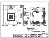
Phase I: AS<strong>IC</strong> Design<br />
When customers have received design<br />
rules, cell libraries, etc., they<br />
can start the AS<strong>IC</strong> design. AS<strong>IC</strong> design<br />
can be split up into front-end<br />
design and back-end design. Frontend<br />
design covers AS<strong>IC</strong> specification<br />
feasibility study and design including<br />
tasks such as schematic<br />
entry, VHDL description, scan insertion,<br />
simulation and synthesis. The<br />
front-end design can be carried out<br />
by the customer himself or can be<br />
subcontracted to a design house.<br />
During this design phase, <strong>Europractice</strong><br />
offers technical support on<br />
technology, test, type of package,<br />
etc. Important know-how and feedback<br />
from the test house will be<br />
used to improve the DFT (Design<br />
For Testability). ”State-of-the-art”<br />
CAD tools are used during the AS<strong>IC</strong><br />
design phase.<br />
Design House know-how<br />
Design for testability (DFT)<br />
Foundry, IP provider<br />
Design rules, IP & cell libraries<br />
models<br />
Foundry, IP provider<br />
IP cell libraries layout<br />
Foundry<br />
Golden rules file<br />
for DRC, LPE, LVS<br />
Critical design review<br />
Tape out<br />
Correct GDS-II database for manufacturing<br />
4 europractice | a total solution<br />
><br />
><br />
><br />
><br />
><br />
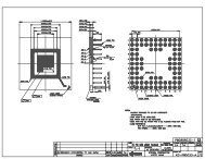
When the netlist is ready the backend<br />
design activity starts including<br />
layout generation using state-ofthe<br />
art layout tools. Deep submicron<br />
digital place & route tasks<br />
are in most cases not performed<br />
by the customers. For those customers<br />
that have not their own<br />
layout tools, EUROPRACT<strong>IC</strong>E is offering<br />
such deep submicron layout<br />
service (see deep submicron layout<br />
service on page 7). After initial<br />
layout, timing verification is carried<br />
out by the customer using<br />
parasitic layout information and<br />
layout is iterated until timing is<br />
met. Verification of the design<br />
needs to be done in all technology<br />
corners.<br />
When layout is finished, a final<br />
DRC (Design Rule Check) and LVS<br />
AS<strong>IC</strong> specifications<br />
Initial design review<br />
Preliminary design review<br />
Digital, analog<br />
front-end design<br />
Physical layout<br />
generation<br />
Design verification<br />
EUROPRACT<strong>IC</strong>E<br />
(Layout versus Schematic) is performed<br />
on the GDS-II database in<br />
order to deliver a correct GDS-II to<br />
the foundry for manufacturing.<br />
customer<br />
design<br />
foundry, IP provider<br />
assembly<br />
test<br />
By courtesy of IMEC
Phase II: Prototyping and test development<br />
After all the checks have been performed<br />
and the GDS-II database is<br />
correct for manufacturing, <strong>Europractice</strong><br />
sends the database to the<br />
foundry for prototyping. Masks will<br />
be generated by the foundry and<br />
first silicon will be produced. Prototyping<br />
can be done on MPW<br />
(Multi Project Wafer) runs or SPW<br />
(Single Project Wafer) pilot runs<br />
(see Low Cost <strong>IC</strong> prototyping on<br />
page 8).<br />
In parallel with prototype fabrication<br />
and prototype packaging the<br />
test solution including test hardware<br />
and software is developed.<br />
EUROPRACT<strong>IC</strong>E will generate<br />
bonding diagram and assembly instructions.<br />
For prototyping ceramic<br />
packages as well as the produc-<br />
When packaged prototypes are<br />
available, they will be shipped to<br />
the test house for debugging. Debugging<br />
includes continuity and<br />
leakage tests, ATPG test and test<br />
of the different analog blocks<br />
(when available on the AS<strong>IC</strong>) at<br />
room (RT) temperature. When prototypes<br />
are working correctly according<br />
to the AS<strong>IC</strong> specification,<br />
low (LT) and high (HT) temperature<br />
are performed. The next stage<br />
is a full characterization of the<br />
AS<strong>IC</strong> at the corners of the voltage<br />
supply and frequency at LT, RT and<br />
HT.<br />
tion plastic packages can be<br />
used. Prototype packaging is<br />
done through one of the assembly<br />
partners in Europe or<br />
the Far-East.<br />
Mask generation<br />
Wafer fabrication<br />
(MPW or engineering lot)<br />
Packaging prototypes<br />
Correct GDS-II database for manufacturing<br />
Prototypes and test solution available<br />
Phase III: First test & Characterization of prototype<br />
During each test a datalog is generated<br />
of the measured values and<br />
histograms and cpk <strong>report</strong>s are<br />
sent to the customer. In case of<br />
specific problems, failure analysis<br />
can be done to determine the reason<br />
of the failing.<br />
By courtesy of Microtest<br />
Test hardware development<br />
Probe card / test board<br />
Test software<br />
development<br />
Debugging hardware<br />
Prototypes and test solution available<br />
Test and debug<br />
prototypes<br />
Test at<br />
RT, LT, HT<br />
Characterization<br />
prototypes<br />
Datalog, histograms, drift<br />
analysis, CPK, CP<br />
europractice | a total solution<br />
5
Phase IV: Qualification of the AS<strong>IC</strong><br />
When customers only need prototypes<br />
of their AS<strong>IC</strong>, qualification is not needed.<br />
However when prototypes are working<br />
correctly and the customer would like to<br />
have volume production it is the right<br />
time to think about the “product qualification”.<br />
Qualification requirements:<br />
Medical<br />
Industrial<br />
Space<br />
Consumer<br />
<strong>Europractice</strong> offers within their test solution<br />
service a full qualification through<br />
one of the test house partners. The<br />
qualification procedure can range from<br />
Consumer, Industry and Medical till Space qualification according to the Military,<br />
JEDEC standards...<br />
The qualification procedure will be discussed<br />
between <strong>Europractice</strong>, customer<br />
and test house and a full qualification<br />
flow will be prepared. To speed<br />
up the procedure, most of the tests<br />
are running in parallel. Special burn-in<br />
boards will be developed for reliability<br />
tests.<br />
By courtesy of MASER Engineering<br />
Phase V: Volume production & test activities<br />
Once the AS<strong>IC</strong> has been qualified, the AS<strong>IC</strong> is ready for volume production. During<br />
the ramp-up phase, yield and process will be monitored. Once the AS<strong>IC</strong> runs into<br />
higher volume, the test solution can be transferred to test houses in the Far East. In<br />
that case the test boards are copied, the original test board will remain in our European<br />
test houses so that yield and process monitoring is still possible.<br />
6 europractice | a total solution<br />
By courtesy of Microtest<br />
><br />
Start new batch of wafers<br />
Packaging<br />
Development of<br />
qualification procedure<br />
Qualification hardware<br />
development<br />
Qualification software<br />
development<br />
Datalog, histograms,<br />
CPK, CP<br />
Wafer production<br />
Probe test<br />
Packaging<br />
Final test<br />
Yield & process<br />
monitoring<br />
Delivery tested<br />
components
EUROPRACT<strong>IC</strong>E<br />
offers deep submicron design support service<br />
Synthesis and layout of deep submicron chips is not<br />
straightforward. You need a highly trained team of engineers<br />
equipped with expensive state-of-the art software<br />
tools. The chips are growing in size whereas the<br />
technology dimensions are getting smaller. Because of<br />
this, designers have to understand how to tackle issues<br />
like: clock-skew, latencies of interacting clock domains,<br />
IR-drop on the power distribution, electro-migration<br />
and signal integrity issues, handling up to 8<br />
layers of metal in the back-end, incorporating IP blocks<br />
in the design, on-chip variation, design for packaging,<br />
etc.<br />
Supporting high-level designers, EUROPRACT<strong>IC</strong>E <strong>IC</strong> Service<br />
provides a design support service starting from<br />
RTL code or synthesized netlist. The service includes<br />
the whole back-end design flow: virtual prototyping,<br />
physical synthesis, deep-submicron layout, timing<br />
analysis, simulation, ATPG, tape-out preparation, etc.<br />
The service is equipped with state-of-the art tools from<br />
the major vendors: the Synopsys Galaxy and Cadence<br />
Encounter Platforms.<br />
In the past many circuits were taped out successfully<br />
both for in-house developed Systems-On-a-Chip as for<br />
AS<strong>IC</strong>s developed by third party design houses, research<br />
institutes and universities. Many of these circuits<br />
included IP blocks like analog full custom blocks,<br />
memory macro’s (even from different vendors), special<br />
I/O and RTL level (soft or firm) IP.<br />
Procedures are in place to offer standard and staggered<br />
I/O configurations and configurations with bonding<br />
pads equally spread over the standard-cell core, for<br />
flip-chip application.<br />
Some circuit complexities handled are: up to 71 million<br />
transistors, several hundred interrelated gated clock<br />
domains and technologies from many different vendors<br />
down to 90nm.<br />
Layout of a 40 million transistor circuit featuring RAMS and other<br />
IP in Chartered Semiconductor 0.13µ CMOS – 46.5 mm 2<br />
(By courtesy of IMEC)<br />
Layout of a 3.7 million-transistor circuit featuring several memory<br />
blocks and PLL in UMC 0.18µ CMOS (6 metal layers) – 20 mm 2<br />
(By courtesy of IMEC)<br />
europractice | a total solution<br />
7
Low cost <strong>IC</strong> prototyping<br />
The cost of producing a new AS<strong>IC</strong><br />
for a dedicated application within<br />
a small market can be high, if directly<br />
produced by a commercial<br />
foundry. This is largely due to the<br />
NRE (Non-Recurring Engineering)<br />
overheads associated with design,<br />
manufacturing and test.<br />
EUROPRACT<strong>IC</strong>E has reduced the<br />
NRE, especially for AS<strong>IC</strong> prototyping,<br />
by two techniques:<br />
(i) Multi Project Wafer Runs or<br />
(ii) Multi Level Masks.<br />
Multi Project Wafer Runs<br />
By combining several designs from<br />
different customers onto one mask<br />
set and prototype run, known as<br />
Multi Project Wafer (MPW) runs,<br />
the high NRE costs of a mask set<br />
is shared among the participating<br />
customers.<br />
8 europractice | a total solution<br />
Fabrication of prototypes can thus<br />
be as low as 5% to 10% of the<br />
cost of a full prototyping wafer<br />
run. A limited number of tested or<br />
untested AS<strong>IC</strong> prototypes, typically<br />
20-50, are delivered to the customer<br />
for evaluation, either as<br />
naked dies or as encapsulated devices.<br />
Only prototypes from fully<br />
qualified wafers are taken to ensure<br />
that the chips delivered will<br />
function “right first time”.<br />
In order to achieve this, extensive<br />
Design Rule and Electrical Rule<br />
Checkings are performed on all<br />
designs submitted to the Service.<br />
EUROPRACT<strong>IC</strong>E is organising about<br />
130 MPW runs per year in various<br />
technologies.<br />
Multi Level Mask<br />
Single User Runs<br />
Another technique to reduce the<br />
high mask costs is called Multi<br />
Level Mask (MLM). With<br />
By courtesy of IMEC<br />
this technique the available mask<br />
area (20 mm x 20 mm field) is typically<br />
divided in four quadrants<br />
(4L/R: four layer per reticle) whereby<br />
each quadrant is filled with one<br />
design layer. As an example : one<br />
mask can contain four layers such<br />
as nwell, poly, ndiff and active.<br />
The total number of masks is thus<br />
reduced by a factor of four. By<br />
adapting the lithographical procedure<br />
it is possible to use one<br />
mask four times for the different<br />
layers by using the appropriate<br />
quadrants. Using this technique<br />
the mask costs can be reduced by<br />
about 60%.<br />
The advantages of using MLM single<br />
user runs are : (i) lower mask<br />
costs, (ii) can be started any date<br />
and not restricted to scheduled<br />
MPW runs, (iii) single user and (iv)<br />
customer receives minimal a few<br />
wafers, so a few hundreds of prototypes.<br />
This technique is preferred over<br />
MPW runs when the chip area becomes<br />
large and when the customer<br />
wants to get a higher number<br />
of prototypes or preserie.<br />
When the prototypes are successful,<br />
this mask set can be used<br />
under certain conditions for low<br />
volume production.<br />
This technique is only<br />
available for technologies<br />
from AMI Semiconductor<br />
and IHP.
Technologies<br />
For 2006, EUROPRACT<strong>IC</strong>E has extended its technology<br />
portfolio. Currently customers can have access to prototype<br />
and production fabrication in the following<br />
technologies :<br />
• AMIS 0.35µ C035M-A 5M/2P/HR<br />
• AMIS 0.35µ C035M-D 5M/1P<br />
• AMIS 0.35µ C035M-I3T80U 80 V - 3M & 4M<br />
• AMIS 0.5µ C05M-A 3M/2P/HR<br />
• AMIS 0.5µ C05M-D 3M/1P<br />
• AMIS 0.5µ CMOS EEPROM C5F & C5N<br />
• AMIS 0.7µ C07M-A 2M/1P/PdiffC/HR<br />
• AMIS 0.7µ C07M-D 2M/1P<br />
• AMIS 0.7µ C07M-I2T100 100V 2M & 3M option<br />
• AMIS 0.7µ C07M-I2T30 30 V - 2M<br />
• AMIS 0.7µ C07M-I2T30E 30 V - 2M<br />
• UMC L90N Logic/Mixed-Mode/RFCMOS 1P9M lowK<br />
• UMC L130E FSG 1P8M Cu Logic/Mixed-Mode (HS/SP/LL)<br />
• UMC L130E FSG 1P8M Cu Mixed-Mode/RFCMOS (HS/SP/LL)<br />
• UMC L180 CIS 2P5M + MMC (Color filter + µlens sup.) -<br />
OPTO process<br />
• UMC L180 Logic GII 1P6M 1.8V/3.3V + MMC<br />
• UMC L180 Mixed-Mode/RFCMOS 1.8V/3.3V<br />
• UMC L250 Mixed-Mode/RFCMOS 1P5M 2.5V/3.3V<br />
• austriamicrosystems 0.35µ SiGe-BiCMOS S35 4M/4P<br />
• austriamicrosystems 0.35µ CMOS C35B3C1 3M/2P/5V IO<br />
• austriamicrosystems 0.35µ CMOS C35B4C3<br />
4M/2P/HR/5V IO<br />
• austriamicrosystems 0.35µ CMOS CSI 3M/2P/5V IO<br />
• austriamicrosystems 0.35µ CMOS C35OPTO 4M/2P/5V IO<br />
• austriamicrosystems 0.35µ CMOS w/EEPROM C35 4M/2P<br />
• austriamicrosystems 0.35µ HV CMOS H35 50V 3M & 4M<br />
• austriamicrosystems 0.8µ CMOS CXQ 2M/2P/HR<br />
• austriamicrosystems 0.8µ CXZ 2M/2P/HR 50V<br />
• IHP SG25H1 0.25µ SiGe:C Ft/Fmax=180GHz/220GHz<br />
4M/MIM<br />
• IHP SG25H1/H2/H3/VD with 5th thick metal option<br />
• IHP SG25H2 0.25µ comp. SiGe:C 4M/MIM<br />
• IHP SG25H3 0.25µ SiGe:C Ft/Fmax= 120/140GHz 4M/MIM<br />
• IHP SGB25VD 0.25µ SiGe:C Ft=30GHz@BVCEO>7V+RF<br />
HV-LDMOS<br />
• IHP SGC25B 0.25µ SiGe:C Ft=120GHz/4M/MIM<br />
Supply Partners<br />
IMEC is working together with several partners to<br />
get access to wafer fabrication, assembly and test.<br />
Foundry partners<br />
AMI Semiconductor (AMIS)<br />
austriamicrosystems<br />
IHP<br />
UMC<br />
Assembly partners<br />
ASAT<br />
ASE<br />
Edgetek<br />
HCM<br />
Selmic<br />
Library partner<br />
Virtual Silicon<br />
Test partners<br />
ASE<br />
DELTA<br />
MASER Engineering<br />
Microtec<br />
Microtest<br />
Rood Technology<br />
mini@sic prototyping conditions<br />
for universities and research<br />
laboratories<br />
In order to stimulate universities and research laboratories<br />
to prototype their AS<strong>IC</strong> designs, <strong>Europractice</strong><br />
has introduced in 2003 the concept of mini@sic.<br />
That means that <strong>Europractice</strong> has selected several<br />
MPW runs in different technologies on which universities<br />
and research labs can prototype very small AS<strong>IC</strong><br />
designs with reduced minimum prototype fee as follows<br />
:<br />
• All MPW runs in AMIS technologies are open to the<br />
mini@sic conditions with minimum prototyping fee<br />
of equivalent of 1 mm2 • Selected MPW runs in selected austriamicrosystems<br />
technologies are open to the mini@sic conditions<br />
with minimum prototyping fee of equivalent of 4 or<br />
5 mm2 • All MPW runs in IHP technologies are open to the<br />
mini@sic conditions with zero minimum prototyping<br />
fee<br />
• Selected MPW runs in UMC 0.18µ and 0.13µ CMOS<br />
mixed/RF technology are open to the mini@sic conditions<br />
with minimum prototyping fee of equivalent<br />
of ~ 2.3 mm2 europractice | a total solution<br />
9
<strong>Europractice</strong> offers full test solution<br />
Electrical Test<br />
• Electrical test of Analog, Digital, Mixed AS<strong>IC</strong>’s<br />
• Single and Multi-site test<br />
• Wafer test under cleanroom class 1000 up to 8” wafers<br />
• Yield and process monitoring<br />
• Final test on each type of package<br />
Reliability and qualification test<br />
The product can be qualified according to the military standards for:<br />
• Space qualification<br />
• Medical qualification<br />
• Industrial qualification<br />
• Consumer qualification<br />
1. Qualification<br />
• Visual Inspection<br />
• High Temperature Operating Life test (HTOL)<br />
• Low Temperature Operating Life test (LTOL)<br />
• High Temperature Bias (HTB)<br />
• Latch-up test<br />
• ESD HBM, CDM<br />
Burn-in and life test<br />
• Static and dynamic burn-in<br />
• Max clockfreq up to 40 MHz<br />
• HTOL<br />
Additional services<br />
• Laser marking<br />
• Dry pack and Vacuum seal<br />
• Barcode labelling<br />
Failure analysis<br />
• Decapsulation of plastic packages<br />
• SEM, SAM, X-ray, EMI imaging<br />
• Optical Microscopy<br />
• Plasma Etching<br />
• Probe Bench & Curve Tracer<br />
10 europractice | a total solution<br />
• Multilayer boards (up to 12 layers)<br />
• Stud probing, V-probes<br />
• Characterisation: Cp and Cpk datalog<br />
2. Package Reliability<br />
• Temperature Cycle Test (TCT)<br />
• Temperature Humidity Bias (THB)<br />
• High Accelerated Stress Testing (HAST)<br />
• Pressure Cooker Test (PCT)<br />
• Gross/Fine Leakage Test<br />
• PIND<br />
• Vibration, centrifuge, solderability<br />
• Moisture level qualification<br />
• Bondpull and die shear<br />
Design kits<br />
Designers need the necessary information<br />
(design rules, electrical parameters,<br />
cell library, etc.) of the chosen technology<br />
before they can start the design phase.<br />
All this information is put together by the foundry in the<br />
so-called ‘design kit’. EUROPRACT<strong>IC</strong>E distributes more<br />
than 55 different design kits and cell libraries of the supported<br />
technologies for most popular CAD tools (Cadence,<br />
Mentor Graphics, Synopsys, Tanner, etc.) on CD-ROM.<br />
Customers can have a copy of the CD-ROM with the cell libraries<br />
& design kits by signing a Non-Disclosure or Design<br />
Kit License Agreement with EUROPRACT<strong>IC</strong>E.
WEB site<br />
http://www.europractice.imec.be<br />
The <strong>Europractice</strong> <strong>IC</strong> Service web site provides full information<br />
such as:<br />
• Technologies<br />
• Specification sheets<br />
• Available and supported cell libraries and design kits<br />
• MPW runs<br />
• MPW prices<br />
• Small volume possibilities<br />
• Deep submicron netlist-to-layout service<br />
• Procedures for registration of designs for prototyping<br />
• Etc.<br />
<strong>Europractice</strong>-online<br />
http://www.europractice-online.be<br />
In 2003 <strong>Europractice</strong> introduced “<strong>Europractice</strong>-online”,<br />
a platform for information exchange. This platform is<br />
hosted by IMEC’s Microelectronics Training Center.<br />
Users can register to access information available on<br />
<strong>Europractice</strong>-online. The information that is available is<br />
grouped per technology and contains:<br />
• Public information<br />
• Confidential information in ‘closed’ domains, accessible<br />
after signature of Non-Disclosure Agreement or<br />
Design Kit License Agreement<br />
• News flashes<br />
• Frequently Asked Questions<br />
• Mailing lists<br />
The user can personalize the mailing lists in such a way that he is automatically informed by e-mail whenever a<br />
new document is posted, news is posted, FAQ is posted, etc. The user can choose for which technologies he will<br />
be notified. As such managers can select to be informed on latest news, whereas designers can ask to be notified<br />
on all new items for a specific technology.<br />
europractice | a total solution<br />
11
Results<br />
MPW prototyping<br />
service<br />
AS<strong>IC</strong>s prototyped on MPW runs<br />
In <strong>2005</strong>, a total of 450 AS<strong>IC</strong>s have<br />
been prototyped. Whereas the number<br />
of designs on MPW runs have<br />
been decreased over the last years,<br />
we are very much pleased to see an<br />
increase again in 2004 and <strong>2005</strong>,<br />
as well as for designs from European<br />
universities, research institutes<br />
as from industry.<br />
69% of the designs are sent in by<br />
European universities and research<br />
laboratories while the remaining<br />
31% of the designs is being sent in<br />
by non-European universities and<br />
companies world-wide.<br />
Geometry mix<br />
Year over year we see a shift towards<br />
newest technologies. Also in<br />
600<br />
500<br />
400<br />
300<br />
200<br />
100<br />
0<br />
<strong>Europractice</strong> Research<br />
15%<br />
Industry + non- European univ/research<br />
2000 2001 2002 2003 2004 <strong>2005</strong><br />
Industry + non-European univ/research 140 159 155 115 128 138<br />
<strong>Europractice</strong> Research 27 46 13 48 52 69<br />
<strong>Europractice</strong> Academic 313 281 237 200 234 243<br />
12 europractice | results<br />
31%<br />
<strong>2005</strong> the same trend is shown. The<br />
majority of the designs is now<br />
being done in 0.35µ and below<br />
(77%) while a few years ago the<br />
majority of the designs was still<br />
done in 0.7/0.8µ.<br />
mini@sic<br />
Very encouraging is the fact that the<br />
mini@sic concept was accepted<br />
very well by universities in <strong>2005</strong><br />
with 139 designs prototyped (90 in<br />
MWP designs in <strong>2005</strong><br />
<strong>Europractice</strong> Academic<br />
54%<br />
2004, 54 in 2003). This is a big increase<br />
and confirms that reducing<br />
the prototyping cost for education<br />
helps to stimulate universities to be<br />
more active in AS<strong>IC</strong> design.<br />
Interesting to see is that under the<br />
mini@sic conditions, the more advanced<br />
technologies are even more<br />
used (due to the drastic price reduction).
160<br />
140<br />
120<br />
100<br />
80<br />
60<br />
40<br />
20<br />
0.25 6%<br />
0<br />
0.25 6%<br />
0.13<br />
0.18<br />
0.25<br />
0.35<br />
0.5 & 0.6<br />
0.7 & 0.8<br />
0.18 21%<br />
MWP designs: technology used: 2004<br />
0.18 20%<br />
MWP designs: technology used: <strong>2005</strong><br />
2004 <strong>2005</strong><br />
0.13 2%<br />
0.13 3%<br />
0.35 45%<br />
0.35 48%<br />
0.18 33%<br />
0.25 3%<br />
0.7/0.8 21%<br />
0.7/0.8 20%<br />
0.13 7%<br />
mini@sic designs per gatelength<br />
0.5/0.6 5%<br />
0.5/0.6 3%<br />
0.7/0.8 9%<br />
By courtesy of IMEC<br />
0.5/0.6 2%<br />
0.35 46%<br />
europractice | results<br />
13
14 europractice | results<br />
0<br />
EUROPRACT<strong>IC</strong>E is offering its services world-wide<br />
EUROPRACT<strong>IC</strong>E has offered since 1996 its low cost AS<strong>IC</strong> MPW<br />
prototyping services to customers from 48 countries worldwide.<br />
As the service is based in Europe, the majority of the<br />
designs come from European customers. But the interest<br />
from non-European countries is growing fast.<br />
100 200 300 400 500 600 700
Small volume projects<br />
More and more customers are using<br />
the COT (Customer Own Tooling)<br />
model when they need volume production.<br />
Through this COT model<br />
they have full control about every<br />
aspect of the total design and production<br />
flow. Large customers with<br />
sufficient AS<strong>IC</strong> starts and volume<br />
production can invest in the COT<br />
model as it requires a considerable<br />
knowledge and experience about all<br />
aspects such as libraries, design<br />
kits, transistor models, testing,<br />
packaging, yield, etc. For smaller<br />
customers the COT model is very attractive<br />
but very difficult due to the<br />
lack of experience. For those customers<br />
EUROPRACT<strong>IC</strong>E offers the solution<br />
by guiding the customers<br />
through the full production flow applying<br />
the COT model. EUROPRAC-<br />
T<strong>IC</strong>E helps you with technical assistance<br />
in the selection of the right<br />
package, setting up the test solution,<br />
yield analysis, qualification, etc.<br />
Netherlands<br />
16<br />
United Kingdom 3<br />
Spain 1<br />
Norway 1<br />
Korea<br />
2<br />
Number of small volume projects per country<br />
Through EUROPRACT<strong>IC</strong>E you can<br />
also experience the benefits of the<br />
COT model.<br />
68 small volume projects in <strong>2005</strong><br />
EUROPRACT<strong>IC</strong>E offers a great benefit<br />
to the foundries by taking care<br />
about the smaller customers, not<br />
being able to commit high volumes.<br />
Although the number of small volume<br />
projects has decreased, the<br />
total wafer volume sold has increased.<br />
This mainly due to the<br />
fact that die size of AS<strong>IC</strong>S is larger<br />
than in previous years.<br />
EUROPRACT<strong>IC</strong>E takes care about<br />
the volume projects requiring annual<br />
volumes up to 1000 wafers and<br />
more. For foundries this is small<br />
business but for many customers<br />
this can be millions of pieces.<br />
In <strong>2005</strong> EUROPRACT<strong>IC</strong>E sold 68<br />
small volume projects in 13 countries<br />
and delivered about 7.5 mil-<br />
USA 1<br />
Australia 3<br />
Germany 21<br />
lion components. The average projects<br />
represents about 35,000<br />
pieces, but we deliver projects with<br />
less than 500 pieces and other projects<br />
with up to millions of pieces.<br />
These projects range from pure<br />
wafer delivery up to fully tested<br />
and qualified components.<br />
Request for quotation<br />
Customers can fill in a simple 2-page<br />
form with the main specifications.<br />
With this information EUROPRAC-<br />
T<strong>IC</strong>E can answer in a few days and<br />
give a first rough price estimation<br />
so that customers can make a first<br />
evaluation. When the full details of<br />
the AS<strong>IC</strong> are known (area, testing,<br />
etc.) a final more accurate price<br />
quotation can be given.<br />
The request form can be accessed<br />
through our WEB site<br />
(www.europractice.imec.be).<br />
Austria 2 Belgium 9<br />
Denmark 4<br />
France 5<br />
europractice | results<br />
15
Examples of AS<strong>IC</strong> projects<br />
AMCHIP3 processor<br />
INFN Ferrara & INFN Pisa, Italy<br />
Contacts:<br />
R. Tripiccione, INFN, Ferrara<br />
(tripiccione@fe.infn.it)<br />
P. Giannetti, INFN Pisa<br />
(paola.giannetti@pi.infn.it)<br />
Technology :<br />
UMC 0.18µ CMOS 1P6M logic<br />
Die size : 99 mm 2<br />
Description<br />
Particle physics experiment are usu-<br />
ally built around high-energy parti-<br />
cle accelerators where primary par-<br />
ticles (such as protons) are made to<br />
collide heads-on, producing large<br />
numbers (hundreds) of secondary<br />
particles. Physicists study the be-<br />
haviour and eventual decay of these<br />
particles, in order to understand in<br />
details their behaviour and confirm<br />
or disprove theoretical models.<br />
In a typical large experiment, such<br />
as the CDF experiment at Fermilab,<br />
near Chicago in the US, shown in<br />
Figure 1, several layers of detectors<br />
produce signals associated to the<br />
passage of each particle, for each<br />
16 europractice | examples<br />
primary interaction. One of the first<br />
task to perform is to associate inde-<br />
pendent signals to tracks, that is to<br />
the paths followed by each particle<br />
within the detector, and then to se-<br />
lect only those events or particles<br />
that the physicists want to study.<br />
Figure 2 shows an event as seen af-<br />
ter the detectors response has been<br />
digitized and plotted. The task is<br />
to identify all the tracks that follow<br />
some specified criteria. This has to<br />
be down for all events, each arriv-<br />
ing at a rate of the order of the mi-<br />
crosecond. There is an obvious way<br />
to perform the job, suggested by the<br />
artist impression of Figure 3. All po-<br />
tentially interesting tracks are enumer-<br />
ated and then compared with the data<br />
arriving from the detector: every time<br />
a match is found, the track is detected,<br />
and recorded for further analysis.<br />
Figure 1. Figure 2.<br />
After digitization, data coming from<br />
the detector is associated to appro-<br />
priately formatted strings of bits,<br />
so, in the micro-electronics world,<br />
we need to match a given bit se-<br />
quence to a string contained in a<br />
large data-base of “legal” strings.<br />
The data-base contains of the order<br />
of one million strings.<br />
This formidable task is performed<br />
by a collection of AMCHIP3 proc-<br />
essor chips, whose basic structure<br />
is that of a content addressable<br />
memory. Memory locations are ini-<br />
tially loaded with a set of “legal”<br />
strings. As the experiment starts<br />
acquiring data, each event is fed<br />
to the AMCHIP. The processor com-<br />
pares in parallel incoming data with<br />
all its stored patterns and - in just<br />
one clock cycle - outputs pointers<br />
to all matching strings contained in<br />
its bank. Many AMCHIP3 processors<br />
are used in parallel: each of them<br />
receives the same input data and<br />
performs its comparison with a par-<br />
tial set of the complete data-base.<br />
A further important function of the<br />
processor is to sort out and format<br />
the output and to provide all func-<br />
tionalities needed to allow a parallel<br />
effort of hundreds of such proces-<br />
sors. Each AMCHIP3 processor han-
dles approximately 5000 database<br />
elements (each of about 100 bits).<br />
The SVT processing system of the<br />
CDF experiment uses about 2000<br />
AMCHIP3 processors.<br />
The processor has been designed<br />
at Instituto Nazionale di Fisica Nu-<br />
cleare, Ferrara using the UMC 0.18<br />
micron technology available through<br />
<strong>Europractice</strong>. The design uses a de-<br />
sign style based on standard cells.<br />
This approach has been shown as<br />
the best compromise between an<br />
FPGA based approach, much faster<br />
in design but poor in performance,<br />
and a full custom design that would<br />
allow packing many more elements<br />
in the content-addressable memory<br />
but would make it hard to migrate<br />
to more advanced technologies, as<br />
they become eventually available<br />
Figure 3.<br />
and economically viable. The design<br />
is very regular in structure: a regular<br />
placement of the standard cells has<br />
been performed and a very highly<br />
packed structure has been realized.<br />
Figure 5.<br />
The AMCHIP3 has been prototyped as<br />
a multi-chip project and, after succes-<br />
ful tests, a dedicated mask set has<br />
been prepared and production has<br />
been started. A photograph of the<br />
AMCHIP3 die is shown in figure 4,<br />
while a processing board containing<br />
several AMCHIP3 processors is shown<br />
in Figure 5.<br />
Why EUROPRACT<strong>IC</strong>E ?<br />
The development and production of the AMCHIP has been performed in<br />
close collaboration with IMEC, that provided several <strong>Europractice</strong> related<br />
services. Very important to us are the possibility to develop a complex proc-<br />
essor at reasonable costs with a multi-project approach, complemented by<br />
the availability to perform small dedicated production runs with the same<br />
technology.<br />
Extremely helpful has also been the support given by IMEC during some<br />
critical phases of the design and the access to a test facility, where proto-<br />
types and production parts have been screened.<br />
europractice | examples<br />
17<br />
Figure 4.
18<br />
AS<strong>IC</strong> of charge sensitive amplifier (CSA) for micro-strip detectors<br />
Moscow Engineering Physics Institute, Moscow, Russia<br />
Contact :<br />
MEPhI, Electronics Department<br />
Kashirskoe shosse 31<br />
Moscow 115409, Russia<br />
Telephone: +7 495 323 9235<br />
Fax: +7 495 324 2111<br />
Eduard Atkin atkin@eldep.mephi.ru<br />
Technology :<br />
AMIS 0.35µ CMOS 2P5M analog<br />
The chip consists of 16 CSAs plus<br />
2 additional rail-to-rail op-amps. Its<br />
design area is 4 x 2 mm 2 .<br />
The basic unit of the chip is being a<br />
folded cascode CSA, optimized for<br />
80Gb/s CML-topology 2:1 multiplexer<br />
Fraunhofer IIS, Erlangen, Germany<br />
Contact :<br />
Jan Sundermeyer<br />
E-mail :<br />
jan.sundermeyer@iis.fraunhofer.de<br />
Technology :<br />
IHP 0.25µ SGC25C<br />
Die size : 0.74 mm 2<br />
A standard 2:1 multiplexer chip in<br />
CML-topology was developed in<br />
the commercially available 200 GHz<br />
SiGe HBT technology by IHP for data<br />
rates of over 80 Gb/s. The data in-<br />
puts are retimed on chip by two flip-<br />
flops. The supply voltage was set to<br />
4~V to give the transistors enough<br />
head room for proper functionality.<br />
For this reason measures to avoid<br />
voltage breakdown on transistors<br />
had to be taken. The multiplexer<br />
was provided with a cascode output<br />
stage to reduce the voltage stress<br />
on the transistors. The architecture<br />
europractice | examples<br />
detector capacitances up to 100 pF. Its input PMOS<br />
transistor has a high equivalent channel width (50<br />
mm !) to fit tight specification demands on noise<br />
(2000e ENC), dynamic range (1V), power consump-<br />
tion (1 mW), etc. Two additional op amps can be<br />
used for signal shaping and fast buffering.<br />
Main research goals for CSA chip design were:<br />
• Design and manufacture (via MPW) of a test pur-<br />
pose chip for micro-strip detectors prototyping;<br />
• The study of possibilities and merits of AMIS 0.35<br />
µm C035M-A process;<br />
• Optimization of the structure and biasing of CSA.<br />
For that purpose some CSAs are made different<br />
from each other in the grounding and supply-<br />
ing circuits.<br />
delivers wide bandwidth and gener-<br />
ates little jitter.<br />
A 40~Gb/s sequence is generated<br />
by multiplexing four 10~Gb/s-se-<br />
quences. The positive and negative<br />
output of the 4:1-multiplexer are<br />
delayed with different delay con-<br />
stants to generate two sequences<br />
with little correlation to each other.<br />
The delays are adjusted by phase<br />
adjusters to have synchronous data<br />
at the mux which is tested.<br />
supply voltage: -4.3 V<br />
current consumption: 237 mA<br />
clock power (single ended, begin of<br />
cable): 2 dBm<br />
data level: approx 200 mV<br />
eye opening (vertical): 70 mV<br />
eye amplitude: 231 mV<br />
eye opening (horizontal): 8.97 ps<br />
jitter RMS : 688 fs<br />
jitter p-p : 3.78 ps<br />
Measurements confirmed the chip’s<br />
functionality at 80~Gb/s though the<br />
stimuli signals were not optimal.
HACDAC : very high-resolution (>20 bits) data converter<br />
for space application<br />
SRON, Netherlands Institute for Space Research, Utrecht, The Netherlands<br />
Contact :<br />
Johan Haanstra<br />
E-mail: j.h.haanstra@sron.nl<br />
Technology : AMIS 0.35µ CMOS 2P3M analog<br />
Die size : 12.35 mm 2<br />
Description<br />
SRON Netherlands Institute for Space Research is the center of expertise for<br />
the development and exploitation of satellite instruments for astrophysical<br />
and earth-oriented sciences. The sensitivity of scientific space instruments<br />
made by SRON is continuously increasing and is on the way to reach fun-<br />
damental physical limits. To retrieve the data from the sensors in these<br />
instruments, very sophisticated front-end electronics (FEE) is needed. The<br />
technical requirements of the FEE and the demand for low-power and low-<br />
mass electronics asks the use of full custom radiation hardened AS<strong>IC</strong>s. For<br />
several future space missions, very high resolution (>20 bits), low frequency<br />
analog to digital and digital to analog conversion is needed and the qual-<br />
ity of this conversion is critical to the total instrument system. These data<br />
converters are needed in missions like LISA, which will use a laser inter-<br />
ferometric measurement between three formation-flying satellites to detect<br />
gravitational waves. The satellites are at 5 million km distance from each<br />
other and distance variations as small as 3nm need to be detected.<br />
The ExoMars mission, of which the rover with a seismometer will land on the<br />
planet Mars, is another example of a future ESA mission that needs high-<br />
resolution data conversion.<br />
To prepare for these future ESA missions, a feasibility study addressing the<br />
typical problems of high-resolution data conversion in space applications<br />
was started. Most systems use AC biased sensors, which enable bandpass<br />
sigma delta conversion. However, most bandpass converters are designed<br />
for telecom applications and the resonators used in these converters do<br />
not fit the requirements for instrumentation applications. SRON did design<br />
a new discrete time resonator suitable for high-resolution bandpass sigma<br />
delta conversion and put it on a test chip together with a sample & hold<br />
circuit and a digital block to generate the clock signals and the test op-<br />
tions. The chip was developed in cooperation with Xensor Integration, a<br />
small enterprise focussing on integrated sensors located in Delfgauw, the<br />
Netherlands. The chip was processed in the AMIS 0.35u CMOS process via<br />
the <strong>Europractice</strong> MPW service.<br />
europractice | examples<br />
19
20<br />
20/24 GHz VCO for Ka-band satellite or<br />
ISM-band application<br />
IMST GmbH, Kamp-Lintfort, Germany<br />
Contact :<br />
Olaf Kersten<br />
E-mail : kersten@imst.de<br />
Technology : IHP 0.25µ SG25H1<br />
Die size : 0.36 mm 2<br />
Description<br />
IMST GmbH, Kamp-Lintfort, has de-<br />
signed a 20/24 GHz VCO (Voltage<br />
Controlled Oscillator) for Ka-band<br />
satellite or ISM-band applications.<br />
This development is funded and<br />
supported by the German Space<br />
Agency DLR/BMBF in the framework<br />
of the project KERAMIS “Ceramic<br />
Microwave Circuits for Satellite<br />
Communications” (Project ID = 50-<br />
YB-0317). Development and investi-<br />
gation of multilayer LTCC technology<br />
europractice | examples<br />
and other components like solid<br />
state power amplifier, synthesizer<br />
and re-configurable switch matrix<br />
are further tasks of the KERAMIS<br />
project.<br />
The presented VCO on SiGe is the<br />
first oscillator design aiming to<br />
achieve the following specifications<br />
in the given frequency bands:<br />
Tuning range: ftune = 500 MHz<br />
Tuning voltage: Vtune = 2 … 2.8 V<br />
Output power: Pout = 5 … 10 dBm<br />
Phase noise: Lf < –80 dBc/Hz @<br />
100KHz offset<br />
While not all specifications have been<br />
met in the first cycle a re-design has<br />
already been initiated to fulfil the<br />
requirements. Re-<br />
sults are expected to<br />
be available in early<br />
2006. The SiGe-chip<br />
is intended to be uti-<br />
lized in future satel-<br />
lite multimedia appli-<br />
cations in Ka-band,<br />
while the 20 GHz<br />
range is reserved for<br />
satellites’ down-link<br />
(up-link: 30 GHz). Fi-<br />
nally the VCO will be<br />
encapsulated into a<br />
hermetically sealed<br />
LTCC package to fulfil<br />
space requirements.<br />
This technology will<br />
also be made evalu-<br />
ated for applications<br />
in the 24 GHz ISM-<br />
band.<br />
MARC : Muon Arm<br />
Readout Chip<br />
INFN and Cagliari University<br />
Strada prov.le per Sestu km 1.0<br />
09042 Monserrato (CA), Italy<br />
Contact :<br />
Gianluca Usai, Davide Marras<br />
E-mail : gianluca.usai@ca.infn.it,<br />
davide.marras@ca.infn.it<br />
web address: www.ca.infn.it and<br />
gruppo3.ca.infn.it<br />
Technology : austriamicrosystems<br />
0.6µ CUP<br />
Die size : 10.68 mm 2<br />
Application<br />
The AL<strong>IC</strong>E experiment at CERN is an<br />
experiment devoted to the study of<br />
new states of matter which can be<br />
possibly created in ultra relativistic<br />
heavy ion collisions. The experiment<br />
is one of the main 4 projects installed<br />
at the LHC accelerator at CERN which<br />
will start running in 2007.<br />
The Muon Arm is one of the AL<strong>IC</strong>E<br />
sub-projects devoted to the de-<br />
tection of muon pair produced by<br />
heavy quark resonances as the J/psi<br />
and Y family. The detailed study of<br />
particle production will give evi-<br />
dence to transition to a new state of<br />
matter where the quarks and gluons<br />
(the constituents of protons and<br />
neutrons) will be deconfined (the so<br />
called quark-gluon plasma).<br />
The main part of the Muon Arm is<br />
a set of tracking stations made by<br />
multi-wire proportinal chambers<br />
which measure particle track points<br />
and momentum (with the help of a<br />
magnetic field).
Each chamber has segmented cath-<br />
ode planes (strips or pads) which<br />
produce a charge signal on the pas-<br />
sage of a particle. The charge is col-<br />
lected and converted to a digital<br />
number by the front-end electronics.<br />
AS<strong>IC</strong> description<br />
The front-end electronics of the<br />
Muon Arm tracking chambers is<br />
based on readout modules (called<br />
MANU) located onto the chamber<br />
surface (the first stations) or on its<br />
borders (in the slat topology) and<br />
performs local digitization and nu-<br />
merical compression.<br />
Each MANU module contains four<br />
MANAS chips which are directly con-<br />
nected to the pads and integrate<br />
the charge signal.<br />
The readout chip MARC (Muon Arm<br />
Readout Chip) controls the four<br />
MANAS chip and two serial ADC<br />
AD7476, and performs zero sup-<br />
pression on the data and communi-<br />
cates with a DSP ADSP2106 through<br />
a 4 bit bus developed by Analog<br />
Devices (Link Port). The Threshold<br />
value are stored in a 64 words x 12<br />
bit RAM. The 12 bit ADC words are<br />
latched in a temporary input shift<br />
register and compared with the<br />
RAM words. Data above threshold<br />
are then stored in a 64 words x 18<br />
bit FIFO together with 6 bit channel<br />
address. The data extracted from<br />
the FIFO are merged with the 11 bit<br />
module address word, a parity bit,<br />
and two control bit. The resulting<br />
32 bit word is sent through the Link<br />
Port as 8 nibbles of 4 bit each.<br />
The clock for MARC is generated<br />
using a 16 MHz quartz. The quartz<br />
is connected to an AMS oscilla-<br />
tor standard cell that works in the<br />
range 1-20 MHz. The chip internal<br />
logic must go at 40 MHz and the<br />
logic controlling the Link Port runs<br />
at 80 MHz. A PLL was designed to<br />
multiply the frequency to the de-<br />
sired value. The PLL is based on a<br />
pulse frequency detector and VCO<br />
(voltage controlled oscillator).<br />
The local bus connecting the MANU<br />
modules uses LVTTL logic. The MARC<br />
Link Port output drivers can source/<br />
sink 32 mA. They are realized inter-<br />
nally with 4 - 8 mA tristate drivers.<br />
Externally each output driver has<br />
two pins in the package which must<br />
be tied together in the PCB.<br />
Several modules are connected in<br />
daisy chain and share the same Link<br />
Port bus. In fig. 1 a diagram of the<br />
chip is shown along with the inputs/<br />
outputs. The chip is designed in the<br />
austriamocrosystems 0.6µ CMOS<br />
3.3V technology.<br />
Why <strong>Europractice</strong> ?<br />
Prototypes were made for design<br />
verification through <strong>Europractice</strong>. A<br />
pre-series using MPW production<br />
and plastic packaging was used for<br />
verifying functionality with radia-<br />
tion to be expected in the applica-<br />
tion. The final production of 28,000<br />
parts was done using a single tool-<br />
ing maskset in austriamicrosystems<br />
0.6µ CMOS technology with a cus-<br />
tom asynchronous test solution us-<br />
ing an Agilent 93000 tester.<br />
europractice | examples<br />
21
22<br />
Polymeric chemoresistive<br />
gas sensors<br />
School of Engineering,<br />
University of Warwick,<br />
Coventry CV4 7AL,<br />
United Kingdom<br />
Contacts :<br />
Marina Cole, Jesús García-Guzmán<br />
and Julian W. Gardner<br />
E-mail : Marina.Cole@warwick.ac.uk<br />
Technology :<br />
AMIS 0.7µ CMOS 1P2M analog<br />
Die size : 3300 x 3750 µm 2<br />
Description<br />
The chip is a second generation chip<br />
fabricated through <strong>Europractice</strong> AMIS<br />
0.7µm C07M-A process as a part of<br />
a PhD research project (García-Guz-<br />
mán) conducted at Warwick Univer-<br />
sity for the monitoring of volatile or-<br />
ganic compounds (VOCs) or gases.<br />
The design integrates two polymeric<br />
chemoresistive gas sensors in a nov-<br />
el ratiometric configuration, togeth-<br />
er with smart circuitry, into a single<br />
chip. The circuit provides automatic<br />
compensation of signal from vari-<br />
ations in both supply voltage and<br />
ambient temperature. On-chip con-<br />
trol of the operating temperature of<br />
the sensors is also an option. As<br />
part of the research programme,<br />
the response of the ratiometric set<br />
of polymeric chemoresistors to dif-<br />
ferent concentrations of gases at<br />
different temperatures and humidi-<br />
ties was simulated with the aid of<br />
a novel parametric Cadence model<br />
(also developed at Warwick) prior to<br />
fabrication. Simulations confirmed<br />
that the ratiometric configuration is<br />
less sensitive to temperature vari-<br />
europractice | examples<br />
ations and that it also has a better<br />
performance in terms of humidity<br />
dependence when compared to in-<br />
dividual chemoresistors.<br />
Figure1 shows the overall structure<br />
of the new smart gas sensor sys-<br />
tem. The main component is the<br />
AS<strong>IC</strong> chip, which performs two ba-<br />
sic functions: (a) sensing the gas<br />
presence and concentration, and<br />
(b) controlling the operating tem-<br />
perature of the gas sensor. Within<br />
the AS<strong>IC</strong> chip, the top section cor-<br />
responds to the gas sensor circuit,<br />
whereas the bottom sections corre-<br />
spond to temperature control and<br />
monitoring. A micro-controller unit<br />
is used for processing the inputs<br />
and outputs of the AS<strong>IC</strong> chip. Ad-<br />
ditionally, three digitally controlled<br />
potentiometers (available in the Xi-<br />
cor’s X9258 integrated circuit) are<br />
used in order to accomplish some<br />
specific trimming functions. The<br />
performance of the first generation<br />
chip agreed with simulations and<br />
the detailed design description and<br />
test results have been published in<br />
the following references:<br />
1. Garcia-Guzman J., Ulivieri N., Cole<br />
M., and Gardner J.W., Design and<br />
simulation of a smart ratiometric<br />
AS<strong>IC</strong> chip for VOC monitoring, Sen-<br />
sors and Actuators B, 95 (2003),<br />
pp. 232-243.<br />
2. Gardner, J.W., Garcia-Guzman, J. and<br />
Cole, M., Smart AS<strong>IC</strong> chip for va-<br />
pour detection based upon carbon<br />
black/polymer composite nanoma-<br />
terials, Proc. of SPIE Conference<br />
on Smart Electronics, MEMS, Bi-<br />
oMEMS, and Nanotechnology, Vol.<br />
5389, 14-18 March 2004, San Di-<br />
ego, California, USA, pp. 344-354.<br />
Figure 1 : Block diagram<br />
representation of the ra-<br />
tiometric sensor system
PhD designs at KULeuven<br />
Katholieke Universiteit Leuven – KULeuven<br />
ESAT-M<strong>IC</strong>AS department, Leuven, Belgium<br />
Contact :<br />
Michiel Steyaert<br />
E-mail : michiel.steyaert@esat.kuleuven.be<br />
Technology : UMC 0.18µ CMOS 1P6M mixed-mode RF<br />
Die size : 5 x 5 mm 2<br />
The <strong>Europractice</strong> facilities enabled designers of ESAT-M<strong>IC</strong>AS to design circuits dealing with important issues in CMOS<br />
design. The first circuit is related to high-speed sigma delta converters. A new implementation of discrete-time sec-<br />
ond-order Sigma-Delta Converters has been investigated. The novel architecture developped enables the converter<br />
to operate at a higher sampling frequency. This allows the use of a simple filter topology while maintaining a good<br />
accuracy. The second circuit is a CMOS power amplifier for the GHz range. The chosen functionality is class E and<br />
the design makes use of power combining. The third circuit is a 8KByte low-power embedded SRAM with improved<br />
robustness against variability and a built-in delay measurement circuit. Finally, the fourth design consists of an<br />
opto-electrical interface circuit for gigabit optical communication. The circuits contains an integrated photodiode<br />
which captures the light, followed by a transimpedance amplifier to convert the small diode current into a voltage.<br />
A post-amplifier boosts the signal to an on-chip voltage swing of 1.2V and an output buffer drives the 50 Ohm load<br />
of the measurement equipment. All these circuits have been designed in UMC 0.18u within the Cadence environment<br />
and are being tested within our facilities at M<strong>IC</strong>AS Leuven. The obtained results will be published in international<br />
and european microelectronics conferences.<br />
MIMO-OFDM Transceiver Chip<br />
Integrated Systems Laboratory, ETH Zurich, Gloriastrasse 35, CH-8092 Zurich, Switzerland<br />
Contact :<br />
Andreas Burg<br />
E-Mail : apburg@iis.ee.ethz.ch<br />
Technology :<br />
UMC 0.25µ CMOS<br />
Die size : 12.8 mm 2<br />
Description<br />
Multiple-input multiple-output (MIMO) systems employ multiple antennas at both transmitter and receiver to significantly<br />
improve link reliability and throughput of wireless communication systems. These gains come at no additional trans-<br />
mit power or bandwidth expenditure. MIMO is considered the key enabling technology for future wireless local area<br />
networks (WLANs) and wireless local loop systems targeting peak data rates of up to 1 Gbps. While AS<strong>IC</strong>s for the IEEE<br />
802.11a standard have been presented, little is known about suitable VLSI architectures for MIMO-OFDM systems and<br />
the corresponding silicon complexity. Goal of this project was to realize an AS<strong>IC</strong> implementation of a MIMO-OFDM WLAN<br />
transceiver with up to four transmit and receive antennas. The design supports datarates of up to 192 Mbps and consti-<br />
tutes one of the fastest WLAN AS<strong>IC</strong> realizations to date. Its architecture is based on the MIMO-OFDM testbed developed<br />
at ETH and comprises the complete baseband processing part including de/modulation, frequency offset estimation and<br />
compensation, frame start detection, and the MIMO detector. The AS<strong>IC</strong> with a die area of 25 mm 2 was manufactured in a<br />
250nm 1P/5M CMOS technology. The AS<strong>IC</strong> running at a system clock frequency of 80 MHz was sucessfully tested.<br />
europractice | examples<br />
23
24<br />
A zero-IF receiver for WCDMA and WLAN 802.11b<br />
Royal Institute of Technology – KTH, Kista, Sweden<br />
Contact :<br />
Wim Michielsen<br />
E-mail : wmich@imit.kth.se<br />
Technology :<br />
UMC 0.18µ CMOS 1P6M mixed-<br />
mode RF<br />
Die size : 1525 x 1525 µm 2<br />
The following description pertains<br />
to a chip that we, at the Radio and<br />
Mixed Signal Circuit and System De-<br />
sign (RaMSiS) Group from KTH in<br />
Sweden, have designed and fabri-<br />
cated through the EUROPRACT<strong>IC</strong>E<br />
service in February <strong>2005</strong>.<br />
Application<br />
The chipset is a reconfigurable<br />
zero/low-IF analog down-converter<br />
for WCDMA and WLAN 802.11b sig-<br />
nals. It is our first integrated chip<br />
for study of future fourth generation<br />
(4G) wireless multiband reconfig-<br />
urable radio receivers. The aim is to<br />
demonstrate the performance and<br />
europractice | examples<br />
the suitability of a reconfigurable<br />
zero/low-IF architecture.<br />
AS<strong>IC</strong> description<br />
The RF front-end blocks are opti-<br />
mized to cover the 1.7 – 2.5 GHz fre-<br />
quency working range. A multiband<br />
VCO with digital switch for switch-<br />
ing the working frequency band is<br />
placed off-chip. The on-chip compo-<br />
nents comprise a single-ended LNA,<br />
a single-to-differential converter,<br />
mixers, a polyphase filter for the<br />
quadrature signal generation and<br />
output drivers after the mixers.<br />
Implementation<br />
The chip is manufactured in the 0.18<br />
µm MM/RF technology of UMC. We<br />
wanted to see the effect of package<br />
parasitics. So the dies are packaged<br />
into refurbished MLF-24 packages<br />
and mounted on a test PCB board.<br />
Why EUROPRACT<strong>IC</strong>E ?<br />
The UMC MM/RF 0.18µm designkit<br />
conveys the basic needs for our<br />
RF CMOS designs. For university<br />
research purposes it is crucial that<br />
we have access to the cheaper MPW<br />
runs from EUROPRACT<strong>IC</strong>E. We could<br />
also benefit from the packaging serv-<br />
ices from EURPRACT<strong>IC</strong>E. In our case<br />
we obtained the most cost effective<br />
solution by packaging our chips in<br />
refurbished MLF-24 packages with-<br />
out compromising the quality.<br />
Project information<br />
www.imit.kth.se/info/FOFU/ramsis/
Designs at Aalborg<br />
University<br />
Aalborg University<br />
Risc Division, Aalborg, Denmark<br />
Contact :<br />
Jan Mikkelsen<br />
E-mail : jhm@kom.aau.dk<br />
Technology :<br />
UMC 0.25µ CMOS 1P5M mixed-mode RF<br />
Die size : 5 x 5 mm 2<br />
Description<br />
The design contains a number of<br />
different test circuits for different<br />
applications. A few circuits are de-<br />
signed for UWB operation in the<br />
3-5GHz band. Specifically, a very<br />
linear and very low-power multiplier<br />
has been designed for this applica-<br />
tion. Further, the design contains a<br />
number of different power amplifier<br />
implementations. Some of the de-<br />
signs aim for UMTS applications and<br />
both single-stage and two-stage<br />
implementations are implemented.<br />
In addition a number of structures<br />
have been included to evaluate the<br />
cross-coupling between planar in-<br />
ductor structures and specifically<br />
how to measure this correctly.<br />
Samira : 8-way SIMD-Vector floating point<br />
processor<br />
University of Dresden, Germany<br />
Institut Nachrichtentechnik<br />
Contact :<br />
Hendrik Seidel<br />
E-mail : seidel@ifn.tu-dresden.de<br />
Technology :<br />
UMC 0.13µ CMOS 1P8M<br />
Die size : 5 x 5 mm 2<br />
Description<br />
The Samira DSP is an 8-way SIMD-Vector<br />
floating point processor based on a novel<br />
microarchitecture concept. It can be re-<br />
garded as a programmable accelerator for<br />
a number crunching tasks in signal process-<br />
ing applications. The processor consumes<br />
1.8mW/MHz running a single precision float-<br />
ing-point FFT in 1890 cycles. The pure core<br />
power is less than 0.57mW/MHz for clock<br />
rates up to 212MHz. So far a moving jpeg<br />
decoder (15fps, 640x480) has been imple-<br />
mented on the DSP and was attached to a<br />
FPGA to enable connectivity through differ-<br />
ent interfaces like an ethernet interface and<br />
a VGA controller. With 100% responsibility<br />
for the overall design process the Vodafone Chair, TU-Dresden was able to<br />
land a first time right design with <strong>Europractice</strong> <strong>IC</strong> Services.<br />
The SAMIRA design features:<br />
• 17 single-precision floating<br />
point units<br />
• ~ 480k NAND gates (UMC<br />
0.13µm)<br />
• 2.9 Mbit on-chip SRAM<br />
• Multiple memory banks for<br />
synchronous access<br />
• Compressed VLIW decoder<br />
• 120-PQFP package<br />
europractice | examples<br />
25
26<br />
The CASTLE emulated digital array processor<br />
Hungarian Academy of Science<br />
Computer and Automotion Institute<br />
Analogic and Neural Computing Systems Laboratory<br />
Budapest, Hungary<br />
Contacts :<br />
T. Hidvégi, P. Keresztes and P.<br />
Szolgay<br />
E-mail : szolgay@sztaki.hu<br />
Technology :<br />
austriamicrosystems 0.35µ CMOS<br />
Die size : 68 mm 2<br />
Description<br />
Emulated digital CNN approaches fo-<br />
cus on the solution of some problems<br />
occurred in the analog VLSI imple-<br />
mentation of a Cellular Neural Network<br />
Universal Machine (CNN-UM). The ac-<br />
High Performance ADC<br />
VTT, Finland<br />
Contact :<br />
Markku Aberg<br />
E-mail : markku.aberg@vtt.fi<br />
Technology :<br />
austriamicrosystems 0.35µ<br />
(SiGe/HBT BiCMOS - S35)<br />
Die size : 39.96 mm 2<br />
europractice | examples<br />
curacy, the usage of nonlinear tem-<br />
plate operations and the implemen-<br />
tation of multilayer structures are<br />
some of the problems to be solved by<br />
an emulated digital CNN-UM proces-<br />
sor array. The speed of the emulated<br />
digital CNN-UM solution should not<br />
be smaller by 2 order of magnitude<br />
than that of an analog CNN-UM.<br />
A 2 x 3 emulated digital CNN proces-<br />
sor array (CASTLE ARRAY processor<br />
array) was designed and implement-<br />
ed by using a 0.35µ CMOS technolo-<br />
gy with variable accuracy and with a<br />
A high performance analog-to-digital<br />
converter (ADC) has been designed<br />
and implemented. The 10-bit ADC op-<br />
erates at the sampling rate of 2GS/s.<br />
A time-interleaved pipeline topology<br />
is utilized to achieve the required<br />
specifications. The ADC samples over<br />
500 MHz (>1GHz ERBW) input band<br />
and uses digital background calibra-<br />
tion to overcome errors arised from<br />
parallelism. The ADC is optimized in<br />
terms of power consumption which<br />
quanrantees maximum efficiency<br />
in operation. Thus, “low” power<br />
(< 5W@3.0VDD) operation should<br />
be achieved. Low-jitter clock delay-<br />
locked loop (DLL) based generator<br />
was implemented to provide re-<br />
quired high accuracy phases for ADC<br />
fingers. A total timing accuracy of<br />
around 1 ps is required to maintain<br />
1 ns/ virtual CNN cell/iteration speed<br />
supposing 12-bit-accuracy.<br />
The processor array was interfaced to<br />
Aladdin Pro where this hardware-soft-<br />
ware environment provides the same<br />
high-level support to develop ana-<br />
logic CNN algorithms that we have by<br />
using the analog VLSI CNN-UMs.<br />
ENOB value. The DLL was designed in<br />
such manner that jitter is minimised<br />
and a 8 bit skew calibrator was inte-<br />
grated into each clock phase output.<br />
The maximum range and resolution<br />
of the skew calibrator are 128 ps and<br />
0.5 ps, respectively.<br />
The ADC chip was laid out using an<br />
0.35 µm SiGe technology by Austria<br />
Microsystems. The chip measures 6.9<br />
x 5.8 mm and consists totally around<br />
200 000 components. The ADC has al-<br />
ready processed and the measurement<br />
results will be available Q2/2006.<br />
Project participants: Helsinki University<br />
of Technology, VTT and Nokia<br />
Acknowledgements: This work has been<br />
supported by European Space Agency,<br />
contract nr. AO/1-3939/01/NL/JSC.
Thrane&Thrane’s Explorer500 :<br />
broadband satellite terminal<br />
Thrane&Thrane, Denmark<br />
Contact :<br />
Allan Sørensen<br />
E-mail : ATS@thrane.com<br />
Technology :<br />
UMC 0.18µ CMOS<br />
Introduction<br />
Inmarsat, specialist in Satellite communication, has<br />
launched its first satellite for Broadband Global Area<br />
Network (BGAN) services. This service is accessible via<br />
a small lightweight, satellite terminal, which is easy to<br />
carry, quick to set up, simple to use, and the same device<br />
can be used worldwide. One of such terminals is the<br />
Explorer 500 from Thrane&Thrane (Denmark), the world’s<br />
leading manufacturer of terminals and land earth stations<br />
for global mobile satellite and radio communications.<br />
Applications<br />
Explorer500<br />
The Explorer500 combines exceptional per-<br />
formance with portability. It meets the<br />
needs of the most demanding business<br />
traveler for remote, high-speed access<br />
to corporate networks. With the same<br />
device you get access worldwide. The<br />
Explorer500 is very small, less than 22<br />
x 22 x 5.5 cm and weighs only 1.5 kg.<br />
The Explorer500 is able to offer remote access, high speed<br />
internet access (up to 464 kbps), email, telephony, streaming<br />
and file transfer. The key benefits are simultaneous voice<br />
and broadband data, global coverage, easy to use, highly<br />
flexible (supports circuit-switched and IP packet data via<br />
standard LAN, USB, Bluetooth and phone/fax interfaces).<br />
The baseband AS<strong>IC</strong><br />
Thrane&Thrane performed the front-end VHDL design and<br />
test vector generation while IMEC provided RTL-to-layout<br />
service, prototyping and volume production logistics, includ-<br />
ing wafer forecast, production and packaging. The selected<br />
technology is the well-proven UMC 0.18µ logic CMOS tech-<br />
nology. The package is a BGA452 Ball-Grid Array. The devel-<br />
opment was quite successful and resulted in first-time-right<br />
prototypes (although the die was larger than 200 mm 2 ).<br />
Production ramp-up<br />
After successful prototyping, IMEC and Thrane&Thrane care-<br />
fully planned the forecast for ramp-up with UMC in order<br />
to get delivery of first Explorer500 terminals to the market<br />
on time when Inmarsat’s BGAN service became operational<br />
by the end of <strong>2005</strong>. Currently IMEC is delivering several<br />
thousands of AS<strong>IC</strong>s per month to Thrane&Thrane.<br />
Why <strong>Europractice</strong> ?<br />
The satellite communication service is still a very niche<br />
market where the terminal providers sell less than 100k<br />
units per year. On the other hand the required AS<strong>IC</strong>s are<br />
quite complex and need the most advanced technolo-<br />
gies such as the UMC 0.18µ CMOS technology. Getting<br />
access to the larger foundries such as UMC for small vol-<br />
umes is very difficult. <strong>Europractice</strong> provided the service<br />
needed and the access to the foundry.<br />
europractice | examples<br />
27
UMC<strong>IC</strong>2 : new design structures for chip-to-chip communication,<br />
power optimization and fault-tolerant design<br />
Ecole Polytechnique Fédérale de Lausanne (EPFL)<br />
Microelectronic Systems Laboratory (LSM)<br />
CH - 1015 Lausanne<br />
Switzerland<br />
http://lsm.epfl.ch<br />
Contact :<br />
Prof. Yusuf Leblebici<br />
E-mail : yusuf.leblebici@epfl.ch<br />
Technology :<br />
UMC 0.18µ CMOS 1P6M mixed-mode<br />
Die size : 5x5 mm 2<br />
The Microelectronic Systems Labo-<br />
ratory of the Ecole Polytechnique<br />
Fédérale de Lausanne (EPFL) has<br />
a research focus on next-genera-<br />
tion digital and mixed-signal VLSI<br />
circuits, covering topics from high-<br />
performance digital logic styles over<br />
chip-to-chip communications and<br />
power optimization to fault-tolerant<br />
design styles for nanometer-scale<br />
technologies.<br />
Why <strong>Europractice</strong>?<br />
Such a vast coverage of research<br />
topics requires access to flexible<br />
and affordable technologies. The<br />
moderate cost of integration, com-<br />
bined with first-class customer sup-<br />
port and a large number of runs per<br />
year in state-of-the-art technologies<br />
minimizes the manufacturing risks<br />
and guarantees short design cycles.<br />
AS<strong>IC</strong> Description<br />
The main parts of the presented cir-<br />
cuit are a novel multi-channel clock<br />
recovery system, limiting amplifiers<br />
for multi-channel fiber-optic commu-<br />
nication links and a power manage-<br />
28 europractice | examples<br />
ment controller for advanced power<br />
management of digital cores. Fur-<br />
ther more, it includes several test<br />
blocks for high-performance A/D<br />
conversion, ultra low-power stand-<br />
ard cell design and opto-electronic<br />
conversion. The extremely low area<br />
and low-power multi-channel clock<br />
and data recovery (CDR) circuit fully<br />
benefits of the small feature size<br />
and the speed offered by this digital<br />
technology to achieve<br />
2.5-Gbps/channel data retiming<br />
with a power consumption of only<br />
3.5mW/Gbps. The power manage-<br />
ment controller implements a novel<br />
on-line energy optimization algo-<br />
rithm, which is capable of dynami-<br />
cally adjusting power supply volt-<br />
ages and operating frequencies of<br />
multiple processing elements as<br />
a function of their instantaneous<br />
workload conditions.
List of Customers per country and number of<br />
designs they have sent in for MPW fabrication<br />
CUSTOMER TOWN Number<br />
of AS<strong>IC</strong>s<br />
Australia<br />
Edith Cowan University Joondalup 11<br />
Motorola Australian Ressearch Centre Botany 1<br />
University of South Wales Sydney 1<br />
Austria<br />
ARC Seibersdorf Research Vienna 1<br />
austriamicrosystems Unterpremstaetten 53<br />
Austrian Aerospace Wien 1<br />
Carinthia Tech Institute Villach-St.Magdalen 1<br />
IEG Stockerau 1<br />
Johannes Keppler University Linz 3<br />
MED-el 2<br />
Securiton Wien 1<br />
TU Wien Vienna 4<br />
Belgium<br />
Alcatel Space Hoboken 4<br />
AnSem Heverlee 2<br />
Browning International SA Herstal 1<br />
Cochlear Technology Centre Europe Mechelen 9<br />
ED&A Kapellen 3<br />
Faculte Polytechnique de Mons Mons 7<br />
FillFactory Mechelen 2<br />
<strong>IC</strong>I - Security Systems Everberg 6<br />
IMEC Leuven 114<br />
K.U. Leuven Heverlee 80<br />
Katholieke Hogeschool Brugge-Oostende Oostende 23<br />
KHLim Diepenbeek 6<br />
KHK Geel 4<br />
KIHA Hoboken 2<br />
Macq Electronique Brussel 1<br />
Neurotech Louvain-la-Neuve 1<br />
Q-Star Test nv Brugge 2<br />
SDT International Bruxelles 1<br />
SEBA Service N.V. Grimbergen 1<br />
SIEMENS ATEA Herentals 2<br />
SIPEX Zaventem 4<br />
Societe de Microelectronique Charleroi 1<br />
Universite catholique de Louvain Louvain-la-Neuve 14<br />
Universiteit Gent Gent 52<br />
University of Antwerp Wilrijk 3<br />
Vrije Universiteit Brussel Brussels 62<br />
CUSTOMER TOWN Number<br />
of AS<strong>IC</strong>s<br />
Brazil<br />
CenPRA Campinas 2<br />
CPqD - Telebras Campinas 7<br />
UFPE Recife-PE 1<br />
UNESP/FE-G Guaratingueta - SP 3<br />
UN<strong>IC</strong>AMP- University of Campinas Campinas, SP 17<br />
Universidade de Sao Paulo Sao Paulo-SP 31<br />
Bulgaria<br />
Technical University of Sofia Sofia 2<br />
Canada<br />
Canadian Microelectronics Corporation Kingston, Ontario 9<br />
Epic Biosonics Victoria 4<br />
University of Alberta Edmonton 1<br />
University of Toronto Toronto 1<br />
University of Waterloo Waterloo 1<br />
China<br />
Dept.Computer Science and Technology BeiJing 1<br />
Fudan University Shanghai 2<br />
Microelectronics Center Harbin 1<br />
The University of Hong Kong Hong Kong 4<br />
Hong Kong Univ. of Science & Technology Hong Kong 1<br />
Zhejiang University Yuquan 1<br />
Croatia<br />
University of Zagreb Zagreb 1<br />
Czech Republic<br />
AS<strong>IC</strong>entrum s.r.o. Praha 4 5<br />
Brno University of Technology Brno 2<br />
Czech Technical University-FEE Prague 5<br />
Denmark<br />
Aalborg University Aalborg 22<br />
Algo Nordic A/S Cph 1<br />
Bang & Olufsen Struer 4<br />
DELTA Hoersholm 11<br />
GN-Danavox A/S Taastrup 4<br />
Microtronic A/S Roskilde 10<br />
Oticon A/S Hellerup 9<br />
PGS Electronic Systems Frb. 1<br />
europractice | list of costumers<br />
29
CUSTOMER TOWN Number<br />
of AS<strong>IC</strong>s<br />
Techtronic A/S Roskilde 1<br />
Tecnical University of Denmark Lyngby 38<br />
Thrane&Thrane Lyngby 1<br />
Egypt<br />
Bahgat Group - IEP Cairo 4<br />
Estonia<br />
Tallinn Technical University Tallinn 1<br />
Finland<br />
Detection Technology Inc. Li 1<br />
Fincitec Oy Oulu 4<br />
Helsinki University of Technology Espoo 39<br />
Nokia Networks Espoo 2<br />
Tampere University of Technology Tampere 8<br />
University of Oulu Oulu 12<br />
VTI Technologies Vantaa 2<br />
VTT Electronics Espoo 81<br />
France<br />
Atmel Nantes, Cedex 3 3<br />
C4i Archamps 13<br />
CCESMAA -IXL Talence 2<br />
CEA Grenoble 20<br />
CMP-TIMA Grenoble 7<br />
CNES Toulouse Cedex 01 4<br />
CPPM Marseille 2<br />
Dibcom Palaiseau 1<br />
Dolphin Integration Meylan 4<br />
EADS Defense&security 1<br />
ELA Recherche Meylan 4<br />
ENSEA Cergy Pontoise 2<br />
ENST Paris Paris 2<br />
ESIEE Noisy Le Grand 3<br />
IN2P3 - LPNHE Paris Cedex 5 6<br />
Institut des Sciences Nucleaires Grenoble 5<br />
Institut de Physique Nucleaire Villeurbanne 7<br />
Institut Sup. d Electronique de Bretagne Brest 2<br />
ISEN Recherche Lille cedex 3<br />
LAAS/CNRS Toulouse 4<br />
Labo PCC CNRS/IN2P3 Paris cedex05 2<br />
Laboratoire de l Accelerateur Lineaire Orsay 6<br />
LAPP Annecy-le-Vieux 7<br />
LEA Cesson Sevigne 1<br />
LEPSI Strasbourg 15<br />
LETI-CEA Grenoble 4<br />
LIRMM Montpellier 2<br />
Midi Ingenierie Labege 1<br />
MXM Laboratories Vallauris 3<br />
30 europractice | list of costumers<br />
CUSTOMER TOWN Number<br />
of AS<strong>IC</strong>s<br />
NeoVision France Bagneux 3<br />
PMIPS - IEF Orsay 2<br />
SODERN Limeil-Brevannes 2<br />
SUPAERO Toulouse Cedex 28<br />
Supelec Gif-sur-Yvette 3<br />
TTPCOM Sophia Antipolis 1<br />
Universite Pierre et Marie Curie Paris 4<br />
Vision Integree Nogent sur Marne 3<br />
Germany<br />
AEG infrarot-module 1<br />
ALV-Laser Vertriebsgesellschaft mbH Langen 1<br />
austriamicrosystems Dresden 2<br />
Balluff 1<br />
Bergische Universitaet Wuppertal Wuppertal 1<br />
Biotronik GmbH & Co Erlangen 9<br />
Bruker AXS 1<br />
Bruker Biospin 2<br />
Cairos Technologies Karlsbad 8<br />
Comtech GmbH St. Georgen 3<br />
Daimler-Benz AG Ulm 3<br />
Darmstadt University of Technology Darmstadt 3<br />
Dr. Johannes Haidenhain 1<br />
ESM Eberline Erlangen 1<br />
ETA Erlangen 1<br />
Fachhochschule Aalen Aalen 3<br />
Fachhochschule Augsburg Augsburg 1<br />
Fachhochschule Bremen Bremen 2<br />
Fachhochschule Darmstadt Darmstadt 8<br />
Fachhochschule Dortmund Dortmund 2<br />
Fachhochschule Esslingen Goeppingen 2<br />
Fachhochschule Furtwangen Furtwangen 6<br />
Fachhochschule Giessen-Friedberg Giessen 11<br />
Fachhochschule Koeln Gummersbach 3<br />
Fachhochschule Mannheim Mannheim 1<br />
Fachhochschule Nuernberg Nuernberg 1<br />
Fachhochschule Offenburg Offenburg 16<br />
Fachhochschule Osnabrueck Osnabrueck 4<br />
Fachhochschule Pforzheim Pforzheim 1<br />
Fachhochschule Ulm Ulm 10<br />
Fachhochschule Wilhelmshaven Wilhelmshaven 1<br />
Fachhochschule Wuerzburg Wuerzburg 1<br />
FAG-Kugelfischer Schweinfurt 3<br />
FH Hannover Hannover 3<br />
FH Karlsruhe Karlsruhe 1<br />
FH Niederrhein Krefeld 5<br />
FhG-IIS Erlangen 124<br />
FH-Münster Steinfurt 1<br />
FORMIKROSYS Erlangen 2<br />
Fraunhofer ISC 1
CUSTOMER TOWN Number<br />
of AS<strong>IC</strong>s<br />
Fraunhofer institute silicontechnology Itzehoe 17<br />
Friedrich-Schiller-University Jena 1<br />
GEMAC Chemnitz 7<br />
Geyer Nuernberg 6<br />
GMD St. Augustin 1<br />
GSI Darmstadt 9<br />
iAd GmbH Grosshabersdorf 1<br />
IHP Frankfurt(Oder) 1<br />
IIP-Technologies GmbH Bonn 4<br />
IMKO Micromodultechnik GmbH Ettlingen 3<br />
IMST GmbH Kamp-Lintfort 3<br />
INOVA Semiconductor Munich 1<br />
Institute for Integrated Systemes Aachen 1<br />
Institute of Microsystem Techology Freiburg 2<br />
Jakob Maul GmbH Bad Koenig 1<br />
Johannes Gutenberg-Universitaet Mainz 9<br />
KVG Quatrz Crystal Neckarbisch 1<br />
Hella 1<br />
Lenze GmbH Aerzen 2<br />
LHR Comtech St. Georgen 1<br />
MAN Nüremberg 1<br />
Max Planck Institute Munchen 1<br />
MAZ Brandenburg Brandenburg 2<br />
MEODAT Ilmenau 2<br />
Metzeler Automotive 3<br />
MPI-Halbleiterlabor Munich 2<br />
NeuroConnex Meckenheim 1<br />
Optek Systems Innovations 1<br />
OPTRON<strong>IC</strong>S 1<br />
Phisikalisches Institut Bonn 20<br />
Preh Werke NA 2<br />
Rechner Industrieelektronik GmbH 1<br />
Ruhr-University Bochum Bochum 4<br />
RWTH Aachen Aachen 8<br />
Scanditronix Wellhöfer NA 3<br />
Schleicher GmbH & Co Relais-Werke KG 1<br />
Schleifring und Apparatebau GmbH 1<br />
Sican Braunschweig GmbH Braunschweig 1<br />
Siemens 4<br />
Seuffer Calw-Hirsau 5<br />
Technical University Ilmenau Ilmenau 14<br />
Technical University of Berlin Berlin 11<br />
Trias Krefeld 1<br />
Trinamic Hamburg 1<br />
TU Berlin Berlin 5<br />
TU Chemnitz Chemnitz 11<br />
TU Darmstadt Darmstadt 11<br />
TU Dresden Dresden 17<br />
TU Hamburg-Harburg Hamburg 22<br />
Universitaet Dortmund Dortmund 2<br />
CUSTOMER TOWN Number<br />
of AS<strong>IC</strong>s<br />
Universitaet Hannover Hannover 11<br />
Universitaet Kaiserslautern Kaiserslautern 9<br />
Universitaet Paderborn Paderborn 11<br />
Universität Rostock Rostock 7<br />
University of Bonn Bonn 29<br />
University of Bremen Bremen 26<br />
University of Freiburg Freiburg 3<br />
University of Heidelberg Heidelberg 31<br />
University of Kassel Kassel 5<br />
University of Magdeburg Magdeburg 11<br />
University of Mannheim Mannheim 8<br />
University of Munich Munich 1<br />
University of Oldenburg Oldenburg 1<br />
University of Saarland Saarbruecken 4<br />
University of Siegen Siegen 13<br />
University of Stuttgart Stuttgart 1<br />
University of Ulm Ulm 3<br />
Vishay semiconductor Heilbronn 2<br />
Wellhoeffer Schwarzenbruck 2<br />
Work Microwave GmbH Holzkirchen 1<br />
Greece<br />
ACE Power Electronics LTD AG Dimitrios 1<br />
Aristotle Univ. of Thessaloniki Thessaloniki 4<br />
Athena Semiconductors SA Alimos - Athens 2<br />
Crypto SA Marousi 1<br />
Datalabs Athens 1<br />
Democritus University of Thrace Xanthi 3<br />
Found. for Research and Techn.-Hellas Heraklion 1<br />
InAccess Athens 1<br />
HEL<strong>IC</strong> SA Athens 1<br />
Hellenic Semiconductor Applications Athens 2<br />
Intracom Paiania 1<br />
National Tech. Univ. of Athens Athens 14<br />
NCSR Athens 22<br />
NTNU n/a 2<br />
RETECO LTD. Athens 1<br />
Unibrain SA Athens 1<br />
University of IONNINA Ioannina 2<br />
University of Patras - VLSI Laboratory Rio - Patras 18<br />
Hungary<br />
Hungarian Academy and Science Budapest 1<br />
Peter Pazmany Catholic University Budapest 1<br />
Computer and Automation Inst. Budapest 6<br />
JATE University Szeged 1<br />
India<br />
College of Eng. Guindy Anna Univesity Chennai 1<br />
Indian Institute of Science Bangalore 3<br />
europractice | list of costumers<br />
31
CUSTOMER TOWN Number<br />
of AS<strong>IC</strong>s<br />
IIT Madras Chennai 5<br />
Indian Institute of Science New Dehli 1<br />
VECC Kolkata 3<br />
Ireland<br />
Cork Institute of Technology Cork 3<br />
National University of Ireland Kildare 1<br />
Farran Technology Ballincollig 1<br />
National Microelectronics Research Cent. Cork 15<br />
Parthus Technologies (SSL) Cork 7<br />
TELTEC Cork 1<br />
University College Cork Cork 2<br />
University of Limerick Limerick 9<br />
Waterford Institute of Technology Waterford 7<br />
Israel<br />
CoreQuest Petach Tikva 2<br />
DSP Semiconductors Givat Shmuel 1<br />
Technion - Israel Institute of Techn. Haifa 4<br />
Italy<br />
Alcatel Alenia L’Aquila 1<br />
Alimare SRL Favria Canavese<br />
(Torino) 1<br />
Aurelia Microelettronica S.p.A. Navacchio PISA 18<br />
BIOTRON<strong>IC</strong> SRL San Benedetto 1<br />
Cesvit Microelettronica s.r.l. Prato 2<br />
DEEI - University of Trieste Trieste 2<br />
INFN Bologna 1<br />
INFN Cagliari 1<br />
INFN Catania 4<br />
INFN Ferrara 1<br />
INFN Milano 1<br />
INFN Genova 2<br />
INFN Padova 2<br />
INFN Roma 10<br />
INFN S.Piero a Grado<br />
(PISA) 2<br />
INFN Torino 4<br />
INFN Trieste 7<br />
Instituto di Sanita Roma 1<br />
Instituto Trentino di Cultura Trento 21<br />
ISE Vecchiano 1<br />
LABEN S.p.A. Vimodrone (MI) 3<br />
Optoelettronica Italia Terlago 1<br />
Politecnico di Bari Bari 4<br />
Politecnico di Milano Milano 53<br />
Politecnico di Torino Torino 5<br />
Sincrotrone Trieste SCpA Trieste 3<br />
SITE Technology s.r.l. Oricola 1<br />
32 europractice | list of costumers<br />
CUSTOMER TOWN Number<br />
of AS<strong>IC</strong>s<br />
SYEL S.r.l. Pontadera 1<br />
Universita degli Studi Dell Aquila L Aquila 3<br />
Universita di Torino Torino 7<br />
Università degli Studi di Ancona Ancona 4<br />
Universita degli Studi di Firenze Firenze 2<br />
Universita di Cagliari Cagliari 6<br />
Universita di Catania Catania 38<br />
University of Bologna Bologna 20<br />
University of Brescia Brescia 6<br />
University of Cagliari Monserrato-Cagliari 8<br />
University of Genova Genova 13<br />
University of Modena Modena 1<br />
University of Naples Napoli 1<br />
University of Padova Padova 23<br />
University of Parma Parma 6<br />
University of Pavia Pavia 7<br />
University of Perugia Perugia 6<br />
University of Pisa Pisa 15<br />
University of Rome Tor Vergata Roma 5<br />
University of Siena Siena 2<br />
Japan<br />
Marubeni Solutions Osaka 8<br />
Hokkaido University Sapporo 6<br />
Yamatake Kanagawa 1<br />
Korea<br />
JOSUYA TECHNOLOGY Taejon 1<br />
KAIST Daejeon 1<br />
Korean Elektrotechnology Research Inst. Changwon 1<br />
Macam Co., Ltd Seoul 2<br />
Nurobiosys Seoul 7<br />
Samsung Electro-Mechanics Suwon 1<br />
Seoul National University Seoul 1<br />
Seloco Seoul 10<br />
Malaysia<br />
SunSem Sdn. Bhd. Kuala Lumpur 1<br />
University of Technology Skudai 1<br />
Malta<br />
University Of Malta Msida 14<br />
Mexico<br />
INAOE Puebla 23<br />
Netherlands<br />
Aemics Hengolo 8<br />
Catena Microelectronics BV Delft 1<br />
Cavendish Kinetics s Hertogenbosch 1
CUSTOMER TOWN Number<br />
of AS<strong>IC</strong>s<br />
Delft University of Technology Delft 17<br />
ESA AG Noordwijk ZH 3<br />
Hogeschool Heerlen Heerlen 1<br />
Lucent Technologies Nederland BV Huizen 1<br />
Mesa Research Institute Twente 1<br />
NFRA Dwingeloo 1<br />
Sonion Amsterdam 3<br />
Smart Telecom Solutions 1<br />
SRON Utrecht 4<br />
Technische Universiteit Eindhoven Eindhoven 44<br />
TNO Industrie Eindhoven 1<br />
TNO -FEL The Hague 2<br />
TU Delft Delft 40<br />
University of Amsterdam Amsterdam 1<br />
University of Twente Enschede 5<br />
Xanadu Wireless Utrecht 1<br />
Xensor Integration Delfgauw 3<br />
New Zealand<br />
Industrial Research Ltd Lower Hutt 4<br />
Norway<br />
AME As Horten 1<br />
Nygon Asker 1<br />
IDE AS Oslo 2<br />
Interon Asker 1<br />
Nordic VLSI Trondheim 38<br />
Norwegian Institute of Technology Trondheim 18<br />
SINTEF Trondheim 6<br />
University of Bergen Bergen 6<br />
University of Oslo Oslo 62<br />
Poland<br />
AGH Univ. of Science and Technology Krakow 3<br />
Institute of Electron Technology Warsaw 34<br />
Technical University of Gdansk Gdansk 3<br />
Technical University of Lodz Lodz 4<br />
University of Mining and Metallurgy Krakow 24<br />
University of Technology & Agriculture Bydgoszcz 1<br />
University of Technology - Poznan Poznan 1<br />
Warsaw University of Technology Warsaw 14<br />
Portugal<br />
Acacia Semiconductor Lisboa 6<br />
Chipidea Oeiras 22<br />
INESC Lisboa 16<br />
INETI Lisboa 1<br />
Instituto de Telecomunicacoes Lisboa 28<br />
Instituto Superior Tecnico Lisboa 6<br />
Universidade de Aveiro Aveiro 18<br />
CUSTOMER TOWN Number<br />
of AS<strong>IC</strong>s<br />
University of Minho Guimaraes 4<br />
University of Porto Porto 2<br />
ISEL-IPL LIsboa 1<br />
University of Tras-os-Montes e Alto Vila Real 2<br />
Uninova Caparica 5<br />
Romania<br />
Polytechnic inst. Bucharest Bucharest 1<br />
Russia<br />
MIET-TU Moscow 2<br />
Moscow Engineering Physics Institute Moscow 1<br />
University St Petersburg St Petersburg 3<br />
Serbia and Montenegro<br />
University of Nis Nis 1<br />
Singapore<br />
Agilent Singapore 2<br />
DSO National Laboratories Singapore 6<br />
Slovakia<br />
Inst. of Computer Systems Bratislava 1<br />
Slovak University of Technology Bratislava 3<br />
Slovenia<br />
Iskraemeco d.d. Kranj 19<br />
NOVOPAS Maribor 1<br />
University of Ljubljana Ljubljana 8<br />
South Africa<br />
Solid State Technology Pretoria 4<br />
University of Pretoria Pretoria 16<br />
South America<br />
CNM/Iberchip 74<br />
Spain<br />
Anafocus Sevilla 1<br />
CNM Bellaterra 27<br />
Design of Systems on Silicon Paterna 7<br />
EUSS Barcelona 1<br />
Facultad de Informática UPV/EHU San Sebastián 2<br />
Technical University of Madrid Madrid 3<br />
Univ. Las Palmas Gran Canaria Las Palmas/Gran Canaria 7<br />
Universidad Cartagena 2<br />
Universidad de Cantabria Santander 9<br />
Universidad de Extremadura Badajoz 17<br />
Universidad de Navarra San Sebastian 31<br />
Universidad del Pais Vasco Bilbao 3<br />
europractice | list of costumers<br />
33
CUSTOMER TOWN Number<br />
of AS<strong>IC</strong>s<br />
Universidad Politecnica de Madrid Madrid 1<br />
Universidad Publica de Navarra Pamplona 12<br />
Universitat autonoma de Barcelona Barcelona 10<br />
Universitat de Barcelona Barcelona 24<br />
Universitat Illes Balears Palma Mallorca 3<br />
Universitat Politecnica de Catalunya Barcelona 20<br />
Universitat Rovira i Virgili Tarragona 2<br />
University of Malaga Malaga 2<br />
University of Sevilla - CNM - Sevilla 60<br />
University of Seville Sevilla 17<br />
University of Vigo Vigo 3<br />
University of Zaragoza Zaragoza 16<br />
Sweden<br />
Bofors Defence AB 2<br />
Chalmers University Goteborg 6<br />
Chalmers University of Technology Gothenburg 66<br />
Defence Researh Establishment Linkoping 5<br />
Ericsson Molndal 2<br />
Ericsson Microelectronics Kista 2<br />
Institutet for Rymdfysik Kiruna 1<br />
Imego AB Goteborg 1<br />
Lulea University of Technology Lulea 8<br />
Lund University Lund 164<br />
Malardalens University Vasteras 2<br />
Mid Sweden University Sundsvall 12<br />
Royal Institute of Technology Kista 21<br />
Saab Ericsson Space AB Goteborg 1<br />
SiCon AB Linkoping 4<br />
Svenska Grindmatriser AB Linkoping 3<br />
University of Trollhattan Trollhattan 3<br />
University of Linköping Linköping 151<br />
Uppsala University Uppsala 11<br />
Switzerland<br />
Asulab SA Marin 22<br />
austriamicrosystems 2<br />
Bernafon Bern 1<br />
Biel School of Engineering Biel 8<br />
CERN Geneva 40<br />
CSEM Zurich 2<br />
CT-Concept 7<br />
EPFL Lausanne 147<br />
ETH Zurich Zurich 77<br />
Hochschule Rapperswill Rapperswill 1<br />
HTA Luzern Horw 2<br />
HTL Brugg-Windisch Windisch 2<br />
id Quantique Carouge 6<br />
Landis + Gyr AG 1<br />
Leica Geosystems Heerbrugg 1<br />
34 europractice | list of costumers<br />
CUSTOMER TOWN Number<br />
of AS<strong>IC</strong>s<br />
LEM Plan-les-Ouates 3<br />
MEAD Microelectronics S.A. St-Sulpice 2<br />
M<strong>IC</strong>ROSWISS Rapperswil 2<br />
Paul-Scherrer-Institute Villigen 14<br />
Photonfocus Lachen 3<br />
Sentron AG Lausanne 7<br />
siemens Zug 2<br />
Smart Silicon Systems SA Lausanne 2<br />
Suter <strong>IC</strong>-Design AG Waldenburg 2<br />
University of Neuchatel Neuchatel 8<br />
University of Zurich Zurich 32<br />
Xemics SA - CSEM Neuchatel 33<br />
Taiwan<br />
Feng Chia University Taichung 1<br />
National Cheng Kung University 1<br />
National Tsing Hua University Hsinchu 4<br />
Thailand<br />
Microelectronic Technologies Bangkok 2<br />
NECTEC Bangkok 28<br />
Turkey<br />
ASELSAN Ankara 1<br />
Bilkent University Ankara 5<br />
Bogazici University Istanbul 5<br />
Istanbul Technical University Istanbul 12<br />
Kardiosis Ankara 1<br />
Middle East Technical Univ. Ankara 8<br />
Sabanci University Istanbul 6<br />
Tubitak Bilten Ankara 4<br />
United Kingdom<br />
Aberdeen University Aberdeen 1<br />
Barnard Microsystems Limited London 2<br />
Bournemouth University Poole 3<br />
Bradford University Bradford 7<br />
Brunel university Uxbridge 1<br />
Cadence Design Systems Ltd Bracknell 1<br />
Cambridge Consultants Ltd. Cambridge 3<br />
Cardiff University Cardiff 5<br />
CML Microcircuits Ltd. Maldon 12<br />
Control Technique Newtown 4<br />
Data Design & Developmentsq Stone 1<br />
Dukosi Edinburgh 1<br />
Edinburgh University Edinburgh 38<br />
Epson Cambridge research lab Cambridge 2<br />
ELBIT Systems Ltd. 1<br />
Heriot-Watt University Edinburgh 2<br />
Imperial College London 9
CUSTOMER TOWN Number<br />
of AS<strong>IC</strong>s<br />
Jennic Ltd Sheffield 1<br />
K.J. Analogue Consulting Malmesbury 1<br />
King’s College London London 1<br />
Lancaster University Lancaster 7<br />
Leicester University Leicester 1<br />
Middlesex University London 6<br />
Napier University Edinburgh 4<br />
Nortel Harlow 1<br />
Plextek Ltd Essex 4<br />
Positek Limited Glos 1<br />
CCLRC - RAL Oxon 33<br />
Saul Research Towcester 22<br />
Sheffield Hallam University Sheffield 1<br />
Swindon Silicon Systems Ltd Swindon 3<br />
Tality Livingston 1<br />
The Queens University of Belfast Belfast 3<br />
The University of Hull Hull 1<br />
The University of Liverpool Liverpool 9<br />
UMIST Manchester 43<br />
University College London-UCL London 2<br />
University of Bath 3<br />
University of Birmingham Birmingham 6<br />
University of Brighton Brighton 1<br />
University of Cambridge Cambridge 20<br />
University of Dundee Dundee 1<br />
University of East London London 1<br />
University of Glasgow Glasgow 21<br />
University of Hertfordshire Hatfield 1<br />
University of Kent Canterbury 13<br />
University of London London 38<br />
University of Newcastle upon Tyne Newcastle u/o Tyne 3<br />
University of Nottingham Nottingham 15<br />
University Of Oxford Oxford 17<br />
University of Plymouth Plymouth 2<br />
University of Reading Reading 1<br />
University of Sheffield Sheffield 4<br />
University of Southampton Southampton 18<br />
University of Stirling Stirling 1<br />
University of Surrey Guildford 1<br />
University of the West of England Bristol 2<br />
University of Wales, Aberystwyth Aberystwyth 4<br />
University of Warwick Coventry 4<br />
University of Westminster London 5<br />
Walmsley (microelectronics) Ltd. Edinburgh 1<br />
CUSTOMER TOWN Number<br />
of AS<strong>IC</strong>s<br />
USA<br />
Analog Phoenix 1<br />
austriamicrosystems USA 1<br />
Boston university Boston 1<br />
Brookhaven National Laboratory Upton, NY 1<br />
Columbia University Irvington, NY 15<br />
Discera 1<br />
Duke Universtity Durham 1<br />
Exelys Ilc Los Angeles 2<br />
Flextronics Sunnyvale 1<br />
Fox Electronics Fort Myers 4<br />
General Electric 2<br />
Goddard Space Flight Center, NASA Greenbelt 1<br />
Iwatsu Irving 2<br />
Linear Dimensions, Inc. Chicago 1<br />
Micrel Semiconductor San Jose 3<br />
Microchip Technology 1<br />
MIT - Lincoln Lab Cambridge 4<br />
MOSIS Marina del Rey, CA 18<br />
Nova R&D 1<br />
Parallax Inc. Rocklin 2<br />
Philips Medical Systems Andover 1<br />
Princeton University Princeton, NJ 4<br />
Rockwell Scientific Thousand Oaks, CA 13<br />
Stanford Linear Accelerator Meno Park 11<br />
Symphonix San Jose 5<br />
Tachyon Semiconductor Naperville, IL 2<br />
Tekwiss USA Inc. Costa Mesa 2<br />
Triad Semiconductor 1<br />
University of Chicago Illinois 2<br />
University of Colorado Boulder 1<br />
University of Delaware Newark 3<br />
University of Florida Gainesville 3<br />
University of Pennsylvania Philadelphia, Pa. 2<br />
USRA Washington 1<br />
Vectron International Inc. Hudson, NH 5<br />
Xerox El Segundo 1<br />
Yanntek San Jose, CA 5<br />
europractice | list of costumers<br />
35
All information for MPW runs schedule, prices, etc. is available on-line on our WEB site<br />
www.europractice.imec.be<br />
For more information, please contact one of the EUROPRACT<strong>IC</strong>E service centers.<br />
IMEC<br />
General EUROPRACT<strong>IC</strong>E <strong>IC</strong> office &<br />
<strong>IC</strong> Manufacturing Center<br />
C. Das<br />
Kapeldreef 75<br />
B-3001 Leuven, Belgium<br />
Tel : + 32 16 281 248<br />
Fax : + 32 16 281 584<br />
mpc@imec.be<br />
http://www.europractice.imec.be/<br />
Fraunhofer Institute for Integrated Circuits (Fraunhofer IIS)<br />
Integrierte Schaltungen<br />
<strong>IC</strong> Manufacturing Center<br />
W. McKinley, J. Sauerer<br />
Am Wolfsmantel 33<br />
D-91058 Erlangen, Germany<br />
Tel : + 49 9131 776 401<br />
Fax : + 49 9131 776 499<br />
europrac@iis.fraunhofer.de<br />
http://www.iis.fraunhofer.de/asic/svasic<br />
DESIGN: SHAKKEI.COM