Annual report 2008 - Europractice-IC
Annual report 2008 - Europractice-IC
Annual report 2008 - Europractice-IC

Create successful ePaper yourself
Turn your PDF publications into a flip-book with our unique Google optimized e-Paper software.
Table of contentsForeword ...........................................................................................................................................1 1Your Total and Turn-Key AS<strong>IC</strong> SolutionYour Total and Turn-Key AS<strong>IC</strong> Solution............................................................................................ 33Easy access 3Easy access .............................................................................................................................. 3Phase I: AS<strong>IC</strong> Design 4Phase I: AS<strong>IC</strong> Design ............................................................................................................... 4Phase II: Prototyping and test development 5Phase II: Prototyping and test development .......................................................................... 5Phase III: First test & Characterization of prototype 5Phase III: First test & Characterization of prototype .............................................................. 5Phase IV: Qualification of the AS<strong>IC</strong> 6Phase IV: Qualification of the AS<strong>IC</strong> ......................................................................................... 6Phase V: Volume production & test activities 6Phase V: Volume production & test activities ........................................................................ 6EUROPRACT<strong>IC</strong>E offers deep submicron design support service 7EUROPRACT<strong>IC</strong>E offers deep submicron design support service .............................................. 7Low cost <strong>IC</strong>-prototyping 8Low cost <strong>IC</strong>-prototyping........................................................................................................... 8Technologies / Supply partners / mini@sic 9Technologies / Supply partners / mini@sic.............................................................................. 9EUROPRACT<strong>IC</strong>E offers full test solutions for production 10EUROPRACT<strong>IC</strong>E offers full test solutions for production.........................................................10Web site / EUROPRACT<strong>IC</strong>E-online 11Web site / EUROPRACT<strong>IC</strong>E-online............................................................................................ 11Results 12Results.............................................................................................................................................12MPW prototyping service 12MPW Small prototyping volume projects service........................................................................................................12 15Small volume projects.............................................................................................................13Examples of AS<strong>IC</strong> projects 16Examples List of customers of AS<strong>IC</strong> projects...............................................................................................................16 29AMIS (On Semi).......................................................................................................................16austriamicrosystems................................................................................................................18IHP.......................................................................................................................................... 29UMC........................................................................................................................................ 30List of customers ............................................................................................................................ 332 europractice | table of contents
EUROPRACT<strong>IC</strong>E: :Your Total and Turn-Key AS<strong>IC</strong> SolutionEUROPRACT<strong>IC</strong>E provides provides semiconductor semiconductorand systemNew fablescompaniesstartupwithcompaniesa totalas well as small companies or companiesand turn-key system AS<strong>IC</strong> companies solution with including a total :andhaving small AS<strong>IC</strong> volume products in niche markets experience• and easy turn-key access AS<strong>IC</strong> to foundry solution design including rules, : cell librarieshuge problemsand designtokitsget access to foundriesThrough itssinceagreementtheir volumewith foundriesis too• deep easy access submicron to foundry RTL-to-layout design service rules, small.and library partners, EUROPRACT<strong>IC</strong>E• low cell cost libraries prototype and design fabrication kits serviceis allowed to distribute foundry technology• volume deep submicron fabrication RTL-to-layout service including ser-wafevice fabrication,EUROPRACT<strong>IC</strong>Epackaginghas waferandfoundry agreementsinformationwith differentand cell librariesleadingtest• AS<strong>IC</strong> low cost qualification prototype fabrication service• logistics• technical volume fabrication customer support service includingwafer fabrication, packaging andsuppliers, allowing to offer the mostuponadvancedsimpleassignaturewell asofspecifica standardtechnologiesto those customers. OurNon-Disclosurefoundry partnersAgreementsacknowledgeor a DesigntheEUROPRACT<strong>IC</strong>E Service as the optimal solutionKit Licenseto provideAgreement.wafer capacityto smaller customers. SuppliersThoseagreementssee EUROPRACT<strong>IC</strong>Ecan be downloadedas one bigfromcustomerrepresenting about 600 universitiesthe EUROPRACT<strong>IC</strong>Eand 300 companieswebsite. Inworldwide.thisNew test fables startup companies as well as small companiesThrough agreementsor companieswith foundryway youpartners,have accessEUROPRACT<strong>IC</strong>Ein a few daysishaving • AS<strong>IC</strong> small qualification AS<strong>IC</strong> volume products in niche marketsable to offerexperienceAS<strong>IC</strong> solutionshuge problemsrangingwithoutfrom ahavingfew wafersto gotothroughthousandsa painfulof• logistics to get access to foundries since their volumewafersispertooyear.small.• technical customer supportcustomer qualification procedureat the foundry. Foundry informationEUROPRACT<strong>IC</strong>E has wafer foundry agreements with different leading sup-includes design rules, spice param-pliers, allowing to offer the most advanced as well as specific technologiesEasy accessto those customers. Our foundry partners acknowledge the EUROPRACT<strong>IC</strong>EService as the optimal solution to provide wafer capacity to smaller customers.Suppliers see EUROPRACT<strong>IC</strong>E as one big customer representing aboutThrough its agreement with foundries600 universities and 300 companies world-wide. Through agreements withand library partners, EUROPRACT<strong>IC</strong>E isfoundry partners, EUROPRACT<strong>IC</strong>E is able to offer AS<strong>IC</strong> solutions ranging fromallowed to distribute foundry technologyinformation and cell libraries upona few wafers to thousands of wafers per year.simple signature of a standard Non-Disclosure Agreements or a Design KitLicense Agreement. Those agreementscan be downloaded from the EURO-PRACT<strong>IC</strong>E website. In this way youhave access in a few days withouthaving to go through a painful customerqualification procedure at thefoundry. Foundry information includes most of the popular CAD tools (Cadence,Synopsys, Mentor Graphics,design rules, spice parameters, design& layout manuals and DRC/ERC/LVS Tanner, etc.). This foundry and librarydecks. Cell library information includes information is distributed on the EUlibrarymanuals and design kits for ROPRACT<strong>IC</strong>E CD-ROM or via FTP.Easy accesseters, design & layout manuals andDRC/ERC/LVS decks. Cell library informationincludes library manuals anddesign kits for most of the popularCAD tools (Cadence, Synopsys, MentorGraphics, Tanner, etc.). This foundryand library information is distributedon the EUROPRACT<strong>IC</strong>E CD-ROMor via FTP.europractice | a total solution3
Phase I: AS<strong>IC</strong> DesignWhen When customers have received designrules, cell cell libraries, etc., theycan can start start the the AS<strong>IC</strong> design. AS<strong>IC</strong> desigsigncan can be be split up into front-enddesign and and back-end design. Frontenenddesign design covers covers AS<strong>IC</strong> AS<strong>IC</strong> specification specificasignfeasibility tion feasibility study study and design and design includincludingtasks tasks such as such schematic as schematic entry,in-VHDL entry, description, VHDL description, scan scan insertion, insertion,simulation and synthesis. and synthesis. The front-Thesimulationend front-end design design can be can carried be carried out by the outcustomer by the customer himself or himself can be or subcon-can besubcontracted to a design to a house. design During house.this During design this phase, design <strong>Europractice</strong> phase, <strong>Europractice</strong>technical offers support technical on technology, support onofferstest, technology, type of package, test, type etc. of Important package,know-how etc. Important and know-how feedback and from feedbackhouse from will the be test used house to improve will bethetestthe used DFT to improve (Design the For DFT Testability). (Design”State-of-the-art” For Testability). CAD ”State-of-the-art”tools are usedduring CAD tools the AS<strong>IC</strong> are used design during phase. the AS<strong>IC</strong>When design the phase. netlist is ready the backenddesign activity starts includinglayout generation using state-of-theWhen the netlist is ready the backenddesign activity starts includinglayout generation using state-oftheart layout tools. Deep submicrondigital place & route tasksare in most cases not performedby the customers. For those customersthat have not their ownlayout tools, EUROPRACT<strong>IC</strong>E is offeringsuch deep submicron layoutservice (see deep submicron layoutservice on page 7). After initiallayout, timing verification is carriedlayout by tools. the customer Deep submicron usingartdigital parasitic place layout & route information tasks are andinmost layout cases is iterated not performed until timing by the iscustomers. met. Verification For those of customers the design thathave needs not to their be done own in layout all technology tools, EU-ROPRACT<strong>IC</strong>E corners. is offering such deepsubmicron layout service (see deepsubmicron When layout layout is service finished, on page a final 7).After DRC initial (Design layout, Rule timing Check) verification and LVSis carried out by the customer usingparasitic layout information and(Layout versus Schematic) is performedon the GDS-II database inorder to deliver a correct GDS-II tothe foundry for manufacturing.layout is iterated until timing is met.Verification of the design needs tobe done in all technology corners. By courtesy of IMECWhen layout is finished, a final DRC(Design Rule Check) and LVS (Layoutversus Schematic) is performedon the GDS-II database in order todeliver a correct GDS-II to the foundryfor manufacturing.Design House know-howDesign House know-howDesign for testability (DFT)Design for testability (DFT)Foundry, IP providerDesign Foundry, rules, IP IP& provider cell librariesDesign rules, models IP & cell librariesmodelsFoundry, IP providerIPFoundry, cell libraries IP provider layoutIP cell libraries layoutFoundryGolden Foundry rules filefor Golden DRC, rules LPE, file LVSfor DRC, LPE, LVSCritical design reviewCritical design review>>>>>AS<strong>IC</strong> specificationsAS<strong>IC</strong> specificationsInitial design reviewInitial design reviewPreliminary design reviewPreliminary design reviewDigital, analogfront-end Digital, analog designfront-end designPhysical layoutPhysical generation layoutgenerationDesign verificationDesign verificationcustomercustomerdesigndesignfoundry, IP providerfoundry, IP providerassemblyassemblytesttestTape outTape outEUROPRACT<strong>IC</strong>ECorrect GDS-II database for manufacturingCorrect GDS-II database for manufacturing4 europractice | a total solution
Phase II: Prototyping and test developmentAfter all the checks have been per-performedand the GDS-II database is iscorrect for for manufacturing, Europrac-<strong>Europractice</strong>sends sends the database the database to the to foun-thefoundry for prototyping. for Masks Masks will will begenerated be generated by the by the foundry foundry and and firstsilicon first silicon will be will produced. be produced. Prototyping Prototypingbe done can on be MPW done (Multi on Project MPWcanWafer) (Multi Project runs or Wafer) SPW (Single runs or Project SPWWafer) (Single pilot Project runs Wafer) (see Low pilot Cost runs<strong>IC</strong>prototyping (see Low Cost on page <strong>IC</strong> prototyping 8). onpage 8).In parallel with prototype fabricationand In parallel prototype with packaging prototype fabrica-the testsolution and including prototype test packaging hardware the andsoftware test solution is developed. including EUROPRAC- test hardwarewill and generate software bonding is developed. diagramT<strong>IC</strong>Eand EUROPRACT<strong>IC</strong>E assembly instructions. will generate For prototypingbonding diagram ceramic and packages assembly well instructions.the production For prototyping plastic packages ceramicaspackages as well as the productioncan be plastic used. packages Prototype can packaging beused. is done Prototype through packaging one of the is assemblythrough partners one in of Europe the as-osemblythe Far-East. partners in Europe ordonethe Far-East.Correct GDS-II database for manufacturingCorrect Correct GDS-II GDS-II database database for for manufacturingmanufacturingTest hardware developmentMask generationTest hardware developmentMask Mask generation generationTestProbehardwarecard /developmenttest boardProbe Probe card card / / test test board boardWafer fabricationTest software(MPWWafer Wafer or engineeringfabrication fabrication lot)TestdevelopmentTest software software(MPW (MPW or or engineering engineering lot) lot)developmentdevelopmentPackaging prototypesDebugging hardwarePackaging Packaging prototypes prototypesDebugging Debugging hardware hardwarePrototypes and test solution availablePrototypes Prototypes and and test test solution solution available availablePhase III: First test & Characterization of prototypeWhen packaged prototypes areWhen packaged prototypes areavailable, they will be shipped toavailable, they will be shipped tothe test house for debugging. Debuggingincludes continuity andthe test house for debugging. Debuggingincludes continuity andleakage tests, ATPG test and test ofleakage tests, ATPG test and testthe different analog blocks (whenof the different analog blocksavailable on the AS<strong>IC</strong>) at(when available on the AS<strong>IC</strong>) atroom (RT) temperature.room (RT) temperature. When prototypesare working correctly ac-When prototypes are workingcorrectly according tocording to the AS<strong>IC</strong> specification,the AS<strong>IC</strong> specification, lowlow (LT) and high (HT) temperatureare performed. The next stage(LT) and high (HT) temperatureare performed. Theis a full characterization of thenext stage is a full characterizationof the AS<strong>IC</strong> atAS<strong>IC</strong> at the corners of the voltagesupply and frequency at LT, RT andthe corners of the voltageHT.supply and frequency at LT,RT and HT.During each test a datalog is generatedof the measured values andDuring each test a datalog is generatedof the measured values andhistograms and cpk <strong>report</strong>s are senthistograms and cpk <strong>report</strong>s areto the customer. In case of specificsent to the customer. In case ofproblems, failure analysis can bespecific problems, failure analysisdone to determine the reason of thecan be done to determine the reasonof the failing.failing.By courtesy of MicrotestPrototypes and test solution availablePrototypes Prototypes and and test test solution solution available availableTest and debugTest Test prototypesand and debug debugprototypes prototypesTest atRT,Test Test LT,at at HTRT, RT, LT, LT, HT HTCharacterizationCharacterizationCharacterizationprototypesprototypes prototypesDatalog, histograms, driftDatalog, Datalog, analysis,histograms, histograms, CPK, CPdrift driftanalysis, analysis, CPK, CPK, CP CPeuropractice | a total solution5
ments:>Start new batch of wafersPhase PackagingIV: Qualification of of the AS<strong>IC</strong>When customers customers only only need need prototypesof prototypes theirDevelopmentAS<strong>IC</strong>, of qualification their AS<strong>IC</strong>, of qualificationqualification is not needed. procedureis not needed.Qualification requirements:However when prototypes are workingcorrectly However Qualification and when the prototypes customer hardware would areMedicallike to Qualification requirements:have working volumedevelopmentcorrectly production and the it customerto would think about like to the have “product vol-qualifi-Industrialis the rightMedicaltimeSpace Industrial >cation”. ume Qualification production it software is the rightConsumer Spacetime to think development about the “productqualification”. offers within their test so-Consumer<strong>Europractice</strong>lution Datalog, service a histograms, full qualification through <strong>Europractice</strong> offers within their test solutionone of theCPK,testCPhouse partners. service The a full qualification through one of thequalification procedure can range from test house partners. The qualification proceduretill can Space range qualification from Consumer, according Industry to the Mil-andConsumer, Industry and MedicalMedical itary, till Space JEDEC qualification standards... according to theMilitary, The JEDEC qualification standards... procedure will be discussedbetween procedure <strong>Europractice</strong>, will be discussed cus-The qualificationbetween tomer <strong>Europractice</strong>, and test house customer and and a full test qualificationfull qualification flow will be flow prepared. will be To prepared. speedhouseand aTo speed up up the the procedure, most of of the testsare running are running parallel. in parallel. Special Special burn-in burn-in boardswill be boards developed will for be reliability developed tests. for reliabilitytests.By courtesy of MASER Engineering>Phase V: Volume production & test activitiesPhase V: Volume production & test activitiesOnce the AS<strong>IC</strong> has beenWafer production qualified, the AS<strong>IC</strong> isOnce the AS<strong>IC</strong> has been qualified, the ready AS<strong>IC</strong> for is volume ready for production.will During be monitored. the ramp-up Once the AS<strong>IC</strong> runs intovolume production. Duringthe ramp-up phase, yield and processProbe testhigher volume, the test solution can be phase, transferred yield and to test process houses in the Far East. Inthat case the test boards are copied, will the original be monitored. test board Once will remain in our Europeantest houses so that yield and process the AS<strong>IC</strong> monitoring runs into is higherPackagingstill possible.volume, the test solutioncan be transferredFinal testto test houses in the FarEast. In that case thetest boards are copied,Yield & processthe original test boardmonitoringwill remain in our Europeantest houses so thatDelivery testedyield and process monitoringis stillcomponentsBy courtesy of Microtestpossible.Start new batch of wafersStart new batch of wafersPackagingPackagingDevelopment ofqualification procedureDevelopment ofqualification procedureQualification hardwareQualification development hardwaredevelopmentQualification softwareQualification softwaredevelopmentdevelopmentDatalog, Datalog, histograms, histograms,CPK, CPK, CPWafer productionWafer productionProbe testPackaging Probe testFinal testPackagingYield & processmonitoringFinal testDelivery testedcomponents Yield & processmonitoring6 europractice | a total solutionDelivery testedcomponents
EUROPRACT<strong>IC</strong>Eoffers deep submicron design support serviceSynthesis and layout of deep submicron chips is notstraightforward. You need a highly trained team of engineersequipped with expensive state-of-the art softwaretools. The chips are growing in size whereas thetechnology dimensions are getting smaller. Because ofthis, designers have to to understand how how to tackle to tackle issues issuesclock-skew, like: clock-skew, latencies latencies of interacting of interacting clock clock domains, do-like:IR-drop mains, IR-drop on the on power the power distribution, distribution, electro-migration electro-migrationsignal and integrity signal integrity issues, handling issues, handling up to 8 layers up to of 8andmetal layers in of metal the back-end, in the back-end, incorporating incorporating IP blocks IP blocks in thedesign, in the design, on-chip on-chip variation, variation, design design for packaging, for packaging, etc.etc.Supporting high-level designers, EUROPRACT<strong>IC</strong>E <strong>IC</strong>Service Supporting provides high-level a design designers, support EUROPRACT<strong>IC</strong>E service starting <strong>IC</strong> from Servicecode provides or synthesized a design support netlist. service The service starting includes fromRTLthe RTL whole code or back-end synthesized design netlist. flow: The virtual service prototyping, includesphysical the whole synthesis, back-end deep-submicron design flow: virtual layout, prototyping, timing analysis,physical simulation, synthesis, ATPG, deep-submicron tape-out preparation, layout, etc. timinganalysis, simulation, ATPG, tape-out preparation, etc.The service is equipped with state-of-the art tools fromthe The major service vendors: is equipped the Synopsys with state-of-the Galaxy art and tools Cadence fromEncounter the major Platforms. vendors: the Synopsys Galaxy and CadenceEncounter Platforms.In the past many circuits were taped out successfullyIn the both past for many in-house circuits developed were taped Systems-On-a-Chipout successfullyas both for for AS<strong>IC</strong>s in-house developed developed by third Systems-On-a-Chip party design houses, as forresearch AS<strong>IC</strong>s developed institutes by and third universities. party design Many of houses, these circuitsearchincluded institutes IP blocks and universities. like analog Many full custom of these blocks, cir-re-memory cuits included macro’s IP (even blocks from like analog different full vendors), custom blocks, specialI/O memory and RTL macro’s level (even (soft or from firm) different IP. vendors), specialI/O and RTL level (soft or firm) IP.Procedures are in place to offer standard and staggeredProcedures I/O configurations are in place and to configurations offer standard with and bondingeredpads I/O equally configurations spread over and configurations the standard-cell with core, bond-forstag-flip-chip ing pads application. equally spread over the standard-cell core, forflip-chip application.Some circuit complexities handled are: up to 71 milliontransistors, Some circuit several complexities hundred handled interrelated are: up to gated 71 million clockdomains transistors, and several technologies hundred from interrelated many different gated vendors clockdown domains to 90nm. and technologies from many different vendorsdown to 90nm.IMEC’s flexible-air-interface baseband plaform (TSMC 90nm CMOS)Layout of a 40 million transistor circuit featuring RAMS and other(By courtesy of IMEC)IP in Chartered Semiconductor 0.13µ CMOS – 46.5 mm 2(By courtesy of IMEC)A mixed signal control AS<strong>IC</strong> designed in IMEC’s radiation-hardened-by-DesignLayout of a 3.7 DARE180 million-transistor (UMC 0.18) circuit library featuring for the digital several part memory plusanalog blocks blocks and PLL using UMC layout-based 0.18µ CMOS radiation (6 metal countermeasures.layers) – 20 mm 2(By courtesy of of IMEC)europractice | a total solution7
Low cost <strong>IC</strong> prototypingThe The cost cost of of producing producing a new new AS<strong>IC</strong>for for a a dedicated dedicated application application within within asmall a small market market can can be high, be high, if directly if directlyproduced by a commercial by a commercial foundry.producedThis foundry. is largely This due is largely to the due NRE to (Non- theRecurring NRE (Non-Recurring Engineering) Engineering) overheadsassociated overheads with associated design, with manufacturingmanufacturing and test. anddesign,test.EUROPRACT<strong>IC</strong>E EUROPRACT<strong>IC</strong>E has has reduced reduced the theNRE, NRE, especially especially for for AS<strong>IC</strong> AS<strong>IC</strong> prototyping,by by two two techniques: techniques:ing,(i) (i) Multi Multi Project Project Wafer Wafer Runs Runs or or(ii) (ii) Multi Multi Level Level Masks. Masks.Multi Multi Project Project Wafer Wafer Runs RunsBy By combining combining several several designs designs fromdifferent different customers customers onto onto one one maskset set and and prototype prototype run, run, known known as asMulti Multi Project Project Wafer Wafer (MPW) (MPW) runs,the the high high NRE NRE costs costs of of a mask mask set setis shared among the participatingcustomers.is Fabrication shared among of prototypes the participating can thuscustomers. be as low as 5% to 10% of theFabrication cost of a of full prototypes prototyping can wafer thusbe run. as Alow limited as 5% number to 10% of of tested the cost orof untested a full prototyping AS<strong>IC</strong> prototypes, wafer run. typically A limited20-50, number are delivered of tested to or the untested customerprototypes, for evaluation, typically either 20-50, are asAS<strong>IC</strong>delivered naked dies to or the as customer encapsulated for evaluationvices.either Only as prototypes naked dies from or as fully en-decapsulatedqualified wafers devices. are Only taken prototypesensurefully that qualified the chips wafers delivered are taken willfromto function ensure “right that first the time”. chips deliveredwill function “right first time”.In order to achieve this, extensiveIn Design order Rule to achieve and Electrical this, extensive RuleDesign Checkings Rule are and performed Electrical on Rule allCheckings designs submitted are performed to the on Service. all designsEUROPRACT<strong>IC</strong>E submitted is to organising the Service. aboutEUROPRACT<strong>IC</strong>E 130 MPW runs is per organising year in various about200 technologies. MPW runs per year in varioustechnologies.Multi Level MaskSingle User RunsAnother technique to reduce thehigh mask costs is called MultiLevel Mask (MLM). Withthis Multi technique Level Mask the available maskarea Single (20 User mm x Runs 20 mm field) is typicallyAnother divided technique in four to quadrants reduce the(4L/R: high mask four layer costs per is called reticle) Multi wherebelMask each quadrant (MLM). With is filled this with technique oneLev-design the available layer. As mask an example area (20: mm one xmask 20 mm can field) contain is typically four layers divided suchinas four nwell, quadrants poly, (4L/R ndiff : four and layer active. perThe reticle) total whereby number of each masks quadrant is thusisreduced filled with by one a factor design of layer. four. As Byanadapting example : the one lithographical mask can contain procedurelayers it such is possible as nwell, poly, to use ndiff one andfourmask active. four The times total number for the of different masks islayers thus reduced by using by a the factor appropriate of four. Byquadrants. adapting the Using lithographical this technique proceduremask it is costs possible can to be use reduced one mask bytheabout four times 60%. for the different layers byusing the appropriate quadrants.The Using advantages this technique of using the mask MLM singlecan user be reduced runs are by : about (i) lower 60%. maskcostscosts, (ii) can be started any dateand The advantages not restricted of using to scheduled MLM singleMPW user runs runs, are (iii): single (i) lower user mask and costs, (iv)customer (ii) can be receives started any minimal date and a fewnotwafers, restricted so to a few scheduled hundreds MPW of prototypes.(iii) single user and (iv) customerruns,receives minimal a few wafers, so aThis few hundreds technique of is prototypes. preferred overMPW runs when the chip area becomesThis technique large and is when preferred the customerMPW runs wants when to get the a higher chip area num-be-overber comes of large prototypes and when or the preserie. customerWhen wants the to prototypes get a higher are number success-oful,this mask or preserie. set can be When used theprototypesprototypes under certain are successful, conditions this for mask lowset can volume be used production. under certain conditionsfor low volume production.This technique is onlyThis technique available is for only technologies available fortechnologiesfrom AMIfromSemiconductorAMI Semiconductorand IHP.(now On Semiconductor)and IHP.By courtesy of IMEC8 europractice | a total solution
<strong>Europractice</strong> offers full full test test solution solutionElectrical TestAdditional services• Electrical Electrical test Testof Analog, Digital, Mixed AS<strong>IC</strong>’s• Laser marking• Electrical test of Analog, Digital, Mixed AS<strong>IC</strong>’s• Multilayer boards (up to 12 layers)• Single and Multi-site test• Dry pack and Vacuum seal• Single and Multi-site test• Stud probing, V-probes• Wafer test under cleanroom class 1000 up to 8” wafers• Barcode labelling• Wafer test under cleanroom class 1000 up to 8” wafers • Characterisation: Cp and Cpk datalog• Yield and process monitoring••FinalYieldtestandonprocesseach typemonitoringof packageFailure analysis••MultilayerFinal testboardson each(uptypetoof12packagelayers)• Decapsulation of plastic packages• Stud probing, V-probesReliability and qualification test• Characterisation: Cp and Cpk datalogThe product can be qualified according to the military standards for:• Space qualificationReliability and qualification test• Medical qualificationThe product can be qualified according to• Industrial qualificationthe military standards for:• Consumer qualification• Space qualification• Medical1. Qualificationqualification• Industrial• Visual Inspectionqualification• Consumer• High TemperaturequalificationOperating Life test (HTOL)• Low Temperature Operating Life test (LTOL)• High1. QualificationTemperature Bias (HTB)• Latch-up• Visual Inspectiontest• ESD• HighHBM,TemperatureCDMOperating Life test (HTOL)• Low Temperature Operating Life test (LTOL)• High Temperature Bias (HTB)• Latch-up testBurn-in • ESD and HBM, life CDM test• Static and dynamic burn-in• Probe Bench & Curve Tracer2. Package Reliability• Temperature Cycle Test (TCT)• Temperature Humidity Bias (THB)• High Accelerated Stress Testing (HAST)• Pressure Cooker Test (PCT)• Gross/Fine Leakage Test• PIND• Vibration, centrifuge, solderability• Moisture level qualification• Bondpull and die shear• SEM, SAM, X-ray, EMI imaging• Optical Microscopy• Plasma EtchingDesign kits• Max2. PackageclockfreqReliabilityup to 40 MHzDesigners need the necessary information• HTOL• Temperature Cycle Test (TCT)(design rules, electrical parameters, cellDesign kits• Temperature Humidity Bias (THB)library, etc.) of the chosen technology beforenecessary they can infor-start the design phase.Additional services• High Accelerated Stress Testing (HAST)Designers need the• Laser marking• Pressure Cooker Test (PCT)mation (design rules, All this electrical information parameters,cell library, etc.) foundry of the in the chosen so-called tech-‘design kit’.is put together by the• Dry pack and Vacuum seal• Gross/Fine Leakage Test• Barcode labelling• PINDnology before they EUROPRACT<strong>IC</strong>E can start the design distributes phase. more than 55• Vibration, centrifuge, solderabilityAll this information different is put together design kits by the and foundry cell libraries in the ofFailure analysis• Moisture level qualificationso-called ‘design the kit’. supported EUROPRACT<strong>IC</strong>E technologies distributes for most more popularCAD kits tools and (Cadence, cell libraries Mentor of the Graphics, sup-• Decapsulation of plastic packages• Bondpull and die shearthan 55 different design• SEM, SAM, X-ray, EMI imagingported technologies Synopsys, for most Tanner, popular etc.) CAD on tools CD-ROM. (Cadence,• Optical MicroscopyBurn-in and life testMentor Graphics, Synopsys, Customers Tanner, can have etc.) a on copy CD-ROM. of the CD-ROM• Plasma Etching• Static and dynamic burn-inCustomers can have with a copy the cell of the libraries CD-ROM & design with the kits cell by libraries& design kits ing by a Non-Disclosure signing a Non-Disclosure or Design Kit or License De-sign-• Probe Bench & Curve Tracer• Max clockfreq up to 40 MHz• HTOLsign Kit License Agreement Agreement with with EUROPRACT<strong>IC</strong>E.EUROPRACT<strong>IC</strong>E.10 europractice | a total solution
WEB sitehttp://www.europractice-ic.comhttp://www.europractice.imec.beThe <strong>Europractice</strong> <strong>IC</strong> web Service site web for <strong>IC</strong> site prototyping provides full informationbeen such totally as: renewed and provides full in-hasformation • Technologies such as:• TechnologiesSpecification sheets• Specification Available and sheets supported cell libraries and design kits• Available MPW runsand supported cell libraries and• design MPW prices kits• MPW Small runs volume possibilities• MPW Deep prices submicron netlist-to-layout service• Small Procedures volume for possibilities registration of designs for prototyping• Deep Etc. submicron netlist-to-layout service• Procedures for registration of designs forprototyping• Etc.<strong>Europractice</strong>-online<strong>Europractice</strong>-onlinehttp://www.europractice-online.beIn 2003 <strong>Europractice</strong> http://www.europractice-online.beintroduced “<strong>Europractice</strong>online”,a platform for information exchange.ThisIn 2003platform<strong>Europractice</strong>is hostedintroducedby IMEC’s“<strong>Europractice</strong>-online”,Microelectronicsa platformTrainingfor informationCenter.exchange. This platform ishosted by IMEC’s Microelectronics Training Center.Users can register to access information availableonUsers<strong>Europractice</strong>-online.can register to accessThe informationinformationthatavailableisonavailable<strong>Europractice</strong>-online.is grouped perThetechnologyinformationandthatcontains:is available is•groupedPublic informationper technology and contains:• ConfidentialPublic informationinformation in ‘closed’ domains,•accessibleConfidentialafterinformationsignatureinof‘closed’Non-Disclosuredomains, accessibleafter signatureAgreement or DesignofKitNon-DisclosureLicense AgreementAgreement or• NewsDesignflashesKit License Agreement• FrequentlyNews flashesAsked Questions• MailingFrequentlylistsAsked Questions• Mailing listsThe user can personalize the mailing lists in such a way that he is automatically informed by e-mail whenever anewThe userdocumentcan personalizeis posted,thenewsmailingis posted,lists inFAQsuchis posted,a way thatetc.heTheisuserautomaticallycan chooseinformedfor whichbytechnologiese-mail wheneverhe willabenewnotified.documentAs suchis posted,managersnewscanis posted,select toFAQbeisinformedposted,onetc.latestThe usernews,canwhereaschoosedesignersfor whichcantechnologiesask to behenotifiedwillonbeallnotified.new itemsAs suchformanagersa specificcantechnology.select to be informed on latest news, whereas designers can ask to be notifiedon all new items for a specific technology.europractice | a total solution11
<strong>Europractice</strong> Research<strong>Europractice</strong> Academic273134628113237482005223469243842158729885285ResultsResultsMPW prototypingserviceIndustry + non- European univ/research31%AS<strong>IC</strong>s prototyped on MPW runsAS<strong>IC</strong>s In <strong>2008</strong>, prototyped a total of 534 on MPW AS<strong>IC</strong>s runs haveIn been 2005, prototyped. a total of 450 Whereas AS<strong>IC</strong>s have thebeen number prototyped. of designs Whereas on MPW the numberhave of been designs decreased on MPW over runs the have lastrunsbeen years, decreased we are very over much the pleased last years, towe see are a consolidation very much pleased in <strong>2008</strong>. to see anincrease 69% of the again designs in 2004 are and sent 2005, in byas European well as universities for designs and from research Europeanlaboratories universities, while research the remaining institutes31% of as the from designs industry. is being sent in69% by non-European of the designs universities are sent in and byEuropean companies universities world-wide. and researchlaboratories while the remaining31% Geometry of the mix designs is being sent inby Year non-European over year we universities see a shift and towardsnewest world-wide. technologies. Also incompanies<strong>2008</strong> the same trend is shown. TheGeometry majority of mix the designs is still beingYear done over in 0.35μ year and we see below a shift while towardsnewest technologies. Alsoain600Industry + non-European univ/research 31%<strong>Europractice</strong> Research15%MWP designs in 2005<strong>Europractice</strong> Academic54%<strong>Europractice</strong> Research 16% <strong>Europractice</strong> Academic 53%2005 the same trend is shown. The 2004, 54 in 2003). This is a big increasein <strong>2008</strong>and confirms that reducingmajority of the designs MPW is now designsbeing done in 0.35µ and below the prototyping cost for education(77%) while a few years ago the helps to stimulate universities to bemajority of the designs was still more active in AS<strong>IC</strong> design.done few years in 0.7/0.8µ. ago the majority of the mini@sic Interesting to see is that under thedesigns was still done in 0.7/0.8μ. Very mini@sic encouraging conditions, is the the fact more that the advancedtechnologies concept was are accepted even more verymini@sic The number of designs in 0.35μ is mini@sicVery stable encouraging while the number is the fact of that designs the well used by (due universities to the in drastic <strong>2008</strong> with price 257 reduction).prototyped (207 in 2007).mini@sic 0.25μ technologies concept was and accepted beyond designsGeometry mixvery is increasing. well by 250 universities in 2005with 139 designs prototyped (90 in2002003 2004 20052006 2007 <strong>2008</strong>5004006005001504001003003002005020010001000.8…0.5µ 0.35µ 0.25µ 0.18µ 0.13µ 90nm02000 0 2001 2002 2003 2004 2005 2006 2007 <strong>2008</strong>2000 2001 2002 2003 2004 2005Industry + non-Europeanuniv/research 140 159 155 115 128 138univ/research140 159 155 115 128 138 134 154 164<strong>Europractice</strong> Research 27 46 13 48 52 69<strong>Europractice</strong> Research274613485269848785<strong>Europractice</strong> Academic 313 281 237 200 234 243<strong>Europractice</strong> Academic 313 281 237 200 234 243 215 298 28512 europractice | results
0.18µ 29%0.25µ 15%MPW designs in <strong>2008</strong>technology node and number of designs0.13 2%<strong>Europractice</strong> Research 16% <strong>Europractice</strong> Academic 53%0.18 21%0.13µ 54 90nm 20 0.8...0.5µ 590.18µ 1590.7/0.8 21%Small volume projectsMore and 0.5/0.6 more 5% customers are usingthe COT (Customer Own Tooling)0.25 6%model when they need vol-ume production. Through this COTmodel they have full control aboutevery aspect of the total designand production flow. Large customerswith sufficient AS<strong>IC</strong> starts0.35 45%0.35µ 2090.25µ 43and volume production can investMPW designs in <strong>2008</strong>: technology node and number of designsMWP designs: technology used: 2004in the COT model as it requires aGeometry mixconsiderable knowledge and experience250about all aspects such as0.13 20033%2004 20052006 2007 <strong>2008</strong> libraries, design kits, transistor0.7/0.8 20%0.18 20%models, testing, packaging, yield,200etc. For smaller customers the COT0.5/0.6 3%model is very attractive but very150difficult due to the lack of experience.0.25 6%For those customers EURO-100PRACT<strong>IC</strong>E offers the solution byguiding the customers through thefull production flow applying the50COT model. EUROPRACT<strong>IC</strong>E helps0.35 48%MWP designs: technology used: 2005you with technical assistance inthe selection of the right package,0600setting up the test solution, yield0.8…0.5µ5000.35µ 0.25µ 0.18µ 0.13µ 90nmanalysis, qualification, etc.Geometry mix40030020030010090nm1600 0.132000 2001 0.13µ 2002 2003 2004 2005 2006 2007 <strong>2008</strong>250 0.18Industry + non-Europeanuniv/research140 159 0.18µ 155 115 128 138 134 154 1641400.25<strong>Europractice</strong> Research274613485269848785<strong>Europractice</strong> Academic 313 0.35 281 0.25µ 237 200 234 243 215 298 2852001200.5 & 0.6 0.35µ0.7 & 0.8 0.8…0.5µ100150Through EUROPRACT<strong>IC</strong>E you canalso experience the benefits of theCOT model.0.13 7% 0.7/0.8 9%0.5/0.6 2%0.18 33%mini@sic designs per gatelength0.8…0.5µ 3%800.13µ 11% 90nm 5%0.35µ 37%100600.18µ 159By courtesy of IMEC30090nm0.13µ2500.18µ0.25µ2000.35µ0.8…0.5150100504020 00Industry + non-European univ/research 31%0.25 3%2004 2005 2006 2007 <strong>2008</strong>0.18µ 29%mini@sic designs per gatelengthmini@sic designs per gatelength in <strong>2008</strong>2004 20050.25µ 15%0.35 46%5002004<strong>Europractice</strong> Research 16% <strong>Europractice</strong> Academic 53%MPW designs in <strong>2008</strong>technology node and number of designs0.13µ 54 90nm 20europractice | | results0.8...0.5µ 5913250Geometry mix2003 2004 20052006 2007 <strong>2008</strong>0.18µ 159
AustraliaAustriaBelgiumBrazilCanadaChinaCzech RepublicDenmarkEgyptFinlandFranceGermanyGreeceHungaryIndiaIrelandItalyJapanKorea, RepublicMexicoNetherlandsNorwayPolandPortugalRomaniaRussian FederationSouth AfricaSpainSwedenSwitzerlandThailandTurkeyUnited KingdomUSAAustraliaAustriaBelarusBelgiumBrazilEUROPRACT<strong>IC</strong>E is offering its services world-wideBulgariaEUROPRACT<strong>IC</strong>E has offered since 1996 its low cost AS<strong>IC</strong> MPW CanadaChinaprototyping services to customers from 48 countries worldwide.As the service is based in Europe, the majority of theCroatiaCyprusdesigns come from European customers. But the interest Czech Republicfrom non-European countries is growing fast.DenmarkEgyptEstoniaFinlandFranceGermanyGreeceHungary<strong>Europractice</strong> MPW prototypes in <strong>2008</strong>534 designs being submitted from customers from 34countries. Traditionally a strong activity in all Europeancountries. We notice an increase interest in the<strong>Europractice</strong> service from customers from countrieslike USA and India.IndiaIrelandIsraelItalyJapanKoreaLebanonMalaysiaMaltaMexicoNetherlandsNew ZealandNorwayPolandPortugalRomaniaRussiaSerbia and MontenegroSingaporeSlovakiaSloveniaSouth AfricaSouth AmericaSpainSwedenSwitzerlandTaiwanThailandTurkeyUnited KingdomUSA0 10 20 30 40 50 60 70 80 9000100 200 300 400 500 600 70014 europractice | results
AustraliaAustriaBelarusBelgiumBrazilBulgariaCanadaChinaCroatiaCyprusCzech RepublicDenmarkEgyptEstoniaFinlandFranceGermanyGreeceHungaryIndiaIrelandIsraelItalyJapanKoreaLebanonMalaysiaMaltaMexicoNetherlandsNew ZealandNorwayPolandPortugalRomaniaRussiaSerbia and MontenegroSingaporeSlovakiaSloveniaSouth AfricaSouth AmericaSpainSwedenSwitzerlandTaiwanThailandTurkeyUnited KingdomUSAEUROPRACT<strong>IC</strong>E is offering its services world-wideEUROPRACT<strong>IC</strong>E has offered since 1996 its low cost AS<strong>IC</strong> MPWprototyping services to customers from 48 countries worldwide.As the service is based in Europe, the majority of thedesigns come from European customers. But the interestfrom non-European countries is growing fast.Total designsEUROPRACT<strong>IC</strong>E has offered since 1996 its low cost AS<strong>IC</strong> MPW prototypingservices to customers from 50 countries worldwide. As the service isbased in Europe, the majority of the designs come from European customers.But the interest from non-European countries is growing fast.80 900 100 200 300 400 500 600 700 800 900 10000100 200 300 400 500 600 700europractice | | results15
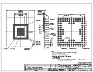
Examples of AS<strong>IC</strong> projectsAMIS(On Semi)P<strong>IC</strong>AM - Planetary Ion CAMeraIMEC, Kapeldreef 75, Leuven, BelgiumContact:Patrick Merken, Ybe CretenTechnology: 0.35µ CMOSDie size: 3200 x 3200 µm 2DescriptionThe P<strong>IC</strong>AM (Planetary Ion CAMera) is an ion mass spectrometer on board ofthe Planetary Orbiter in the ESA/JAXA BepiColombo space mission to Mercury.The mass spectrometry is based on the measurements of ions’ time-offlightto reach an array of micro-channel plate (MCP) detectors.The TIMPO32 detector chip, developed at IMEC, provides front-end amplificationand time-of-flight measurement for 32 MCP detectors. The low powerCharge Pulse Discriminator (CPD) amplifies the charge coming from the detectorand provides the trigger signal in correspondence of which the Timeto-DigitalConverter (TDC) stores the time information with a fine resolution.The CPD has been taped on a 0.35µm CMOS process by ON Semiconductor(AMI Semiconductor). Its dimensions are 3200µm*3200µm.16 europractice | examples
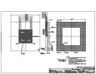
A Low-Power and Accurate CMOS Temperature SensorDelft University of Technology, Electronic Instrumentation Laboratory / DIMES,Mekelweg 4, 2628CD Delft, The NetherlandsContacts:Andre Aita, a.aita@tudelft.nlKofi Makinwa, k.a.a.makinwa@tudelft.nlTechnology: AMIS 0.7µ C07M-A 2M/1P/PdiffC/HRDie size: 4.5 mm 2DescriptionThis AS<strong>IC</strong> was developed as part ofa research project whose aim wasthe realization of low-power CMOStemperature sensors. Such sensorsare based on the well-defined temperaturedependence of the baseemittervoltages of parasitic bipolartransistors. By properly processingthese voltages, a digital representationof temperature can be derived.The AS<strong>IC</strong> consists of a precision biascircuit, which biases two substratePNP transistors in a well-definedmanner, and a 16-bit Delta-Sigma() modulator, which uses theresulting base-emitter voltages togenerate a digital representation oftemperature.The sensor was fabricated through<strong>Europractice</strong> in the AMIS 0.7µ C07M-A process. It draws only 25uA froma 2.5V supply and is fully functionalover a 200˚C temperature range:from -70˚C to 130˚C. Over this range,the sensor’s inaccuracy was lessthan 0.25˚C (3) after a low-costbatch calibration. By trimming individualdevices, the sensor’s inaccuracycould be reduced to less than0.1˚C over the military temperaturerange: -55˚C to 125˚C.More details about the sensor canbe found in a paper published atthe International Solid-State CircuitsConference (ISSCC), A. Aita et al.,“A CMOS Smart Temperature Sensorwith a Batch-Calibrated Inaccuracyof 0.25˚C (3) from -70˚C to130˚C,” Digest of Technical papers,ISSCC, Feb. 2009.Why <strong>Europractice</strong>?Through <strong>Europractice</strong> we gained affordableaccess to a stable CMOSprocess whose options, e.g. linearcapacitors and high ohmic resistors,are especially suited to mixed-signaldesign.europractice | examples17
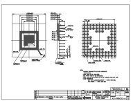
austriamicrosystemsVersatile Endoscopic Capsule for GastrointestinalTumor Recognition and TherapyUniversitat de Barcelona, Atila Herms, Departament d’electronica,Marti Franques 1 - Planta 2, 08028 Barcelona, SpainContact:Oscar AlonsoE-mail: oalonso@el.ub.esTechnology: AMS 0.35 HV-CMOSDie Size: 3.0 x2.7 mm 2DescriptionThe AS<strong>IC</strong> described herewas designed within theframework of the ECproject VECTOR “VersatileEndoscopic Capsulefor Gastrointestinal TumorRecognition andTherapy”. The projectpursues the goal of realizingsmart pill technologiesand applicationsfor gastrointestinal (GI)diagnosis and therapy. The main characteristics of the capsule are that itwill be provided with vision capabilities (as the previous pills) and it will beprovided with locomotion capabilities as well.The AS<strong>IC</strong> contains a complete lens driver composed of one boost converter,several level-shifters and an H-Bridge. This driver is the main part of the visionsystem of the capsule, that it is also composed by some LEDs, a liquidlens and the control electronics. Furthermore, the AS<strong>IC</strong> also contains twocomplete BLDC motor drivers, composed by one charge pump, six levelshiftersand a three-phase inverter. The motor drivers, together with itscontrol electronics, are in charge of the locomotion of the capsule.The technology chosen for the AS<strong>IC</strong> was AMS 0.35 HV-CMOS because it is a reliableand well known technology, and because it is needed to work at 50 V.Why <strong>Europractice</strong>?For the AS<strong>IC</strong> project on small volume the EUROPRACT<strong>IC</strong>E offers design kitservices, frequent MPW runs, it provides valuable help at the last stage ofproject and the affordable mini@sic program.18europractice | examples
A Neural Implant AS<strong>IC</strong> for the Restoration of Balance in Individualswith Vestibular DysfunctionHolistic Electronics Research Laboratory, University of Cyprus 1Institute of Biomedical Engineering, Imperial College London 2Contact:T G Constandinou 1,2 , J. Georgiou 1 , and C. Toumazou 2E-mail: t.constandinou@imperial.ac.ukTechnology: AMS 0.35µm 2P4M CMOS (C35B4C3)Die Size: 3.00 x 3.00 mm 2ApplicationThe vestibular system senses the head’s motion and orientationusing the ampullary (within semicircular canals) and otolith (utricleand saccule) end-organs which help stabilise vision via the vestibulo-ocularreflex (VOR). Vestibular dysfunction often manifests itselfas dizziness, imbalance, blurred vision and instability in locomotion,due to abnormal signalling to the VIII’th cranial (vestibulocochlear)nerve. It is therefore possible, that damage to this system can beovercome by applying similar methodologies to those used in modernneural implants. Specifically, it has been shown that restorationof balance can be achieved by bypassing a dysfunctional element inthe vestibular pathway using artificial stimulation.Circuit DescriptionThis work presents the development of a neural implant AS<strong>IC</strong> forthe restoration of balance in individuals with vestibular dysfunction.The circuit has been fabricated in AMS 0.35µm CMOS and is partof a hybrid CMOS/MEMS realisation to also include the inertia sensorswithin a System-In-Package (SiP) solution. The system senseslinear and radial acceleration in 3-axis (6 degrees of freedom) andimplements multi-stage analogue signal processing to replicate thebiomechanics and neuronal response of the physiological vestibularend-organ within the inner ear. The post-processed signals arethen converted to current-mode representation to drive the multichannelstimulator implementing a Continuous-Interleave-Sampling(CIS) strategy. Additionally, we have implemented an asymmetric,charge-balanced, partial-current-steering scheme to achieve goodstimulation efficiency and to reduce stimulation artefacts whilstmaintaining an acceptable power consumption level. Finally, wehave included appropriate hardware for the calibration, personalisedpatient tuning and related data transfer to ensure robust andfailsafe operation.Why <strong>Europractice</strong>?Both Imperial College London and the Universityof Cyprus are academic members of<strong>Europractice</strong>. Through this, we have accessto a comprehensive MPW fabrication servicein addition to providing us access toindustry-strength EDA tools. The MPW fabricationservice provides highly competitivepricing to a comprehensive range of modernprocess technologies in CMOS, BiCMOS andmore recently MEMS. Without exception,on every occasion, we have found boththe MPW and software services to provideexcellent support, whether it be technical,sales or after-sales.References[1] T. G. Constandinou, J. Georgiou and C. Toumazou, “A Partial-Current-SteeringBiphasic Stimulation Driver for Vestibular Prostheses”, IEEE Transactionson Biomedical Circuits & Systems, Vol. 2, No. 2, pp. 106-113, <strong>2008</strong>.[2] T. G. Constandinou, J. Georgiou and C. Toumazou, “Towards an Integrated,Fully-Implantable Vestibular Prosthesis for Balance Restoration”, TTPAdvances in Science and Technology, pp. 210-215, <strong>2008</strong>.europractice | examples19
High-Frequency Integrated Power Supply on ChipDepartment of Electrical Engineering, University College Cork, IrelandContact:Jason Hannon, Raymond Foley, Kevin McCarthy, Michael EganEmail: raymond.foley@ucc.ieTechnology: AMS 0.35 μm C35B4 CMOSDie size: 3.6 mm x 2.3 mmThe design was created using theCadence DFWII framework and implementedon the AMS 0.35 μmprocess. This was chosen primarilydue to the particular voltage requirementsof the design, thoughdemonstration the design on a bulkCMOS process such as this was alsoan important objective.DescriptionIn recent years, increased miniaturisationand integration in electronicdevices has resulted in expandedfunctionality within shrinking formfactors,particularly in the mobile andhand-held space. From the power deliverypoint of view this has drivena demand for higher power supplydensity and efficiency. Switchingregulators can enable very high efficiency(compared to linear regulators),however the external passivecomponents (inductor and capacitors)they require have an excessivearea and volume overhead at today’stypical operating frequencies (3-8MHz). The aim of this research is todevelop switching regulator technologyoperating at up to 50 MHz inorder to reduce the size of the externalpassives whilst mitigating theeffects of increased switching lossthrough multiple operation modesand on-the-fly optimisation. The particulardesign iteration shown herewas used to explore the benefits ofdynamic switch sizing, load-scheduledfrequency scaling and optimalgate-drive timing parameters. Thedie includes a buck converter powertrain (composed of two independentparallel PMOS top devices and a singleNMOS bottom device), on-chipcapacitive decoupling, low-loss gatedrivecircuitry, a frequency-programmabledigital pulse-width modulator(20 MHz to 50 MHz) and a communication/controlinterface. Results fromthis prototype will be presented atthe Applied Power Electronics Conferencein February 2009.Why <strong>Europractice</strong>?University College Cork is an activemember of EUROPRACT<strong>IC</strong>E, andfabricates a number of <strong>IC</strong>s throughthis route annually. The frequentMPW runs, access to design toolsincluding the AMS HitKit and designsupport/advice makes the processvery attractive to a university-basedresearch group. Furthermore, thequick turn-around time from designfileto chip delivery has enabled usto produce multiple design revisionsin a short time-scale.20europractice | examples
A Sub-μW Fully Tunable CMOS DPS for Uncooled Infrared Fast ImagingIntegrated Circuits and Systems Group, Instituto de Microelectrónica de Barcelona (IMB),Centro Nacional de Microelectrónica (CNM), Consejo Superior de Investigaciones Científicas (CS<strong>IC</strong>)SpainContact:Francesc Serra-GraellsE-mail: paco.serra@cnm.esTechnology: AMS 0.35μm CMOS C35B4C3Die size: 6.2 x 5.1 mm 2DescriptionThere is an increasing demand forinfrared (IR) fast digital imagers inkey application fields like automotive,medical, scientific and strategicequipments. In this sense, the pixelby-pixelcombination of PbSe detectors[1] and digital CMOS read-outcircuits, either by post-processing orbump-bonding, is a promising technologyfor low-cost, uncooled andvery fast (>100fps) IR imagers.This work presents a 32pixel x 32pixel focal plane array (FPA) of digitalactive pixel sensors (DPS) specificallydesigned for uncooled photoconductiveIR detectors. Each DPScell of 130μm x 130μm contains allthe CMOS circuits for input capacitanceand dark current compensation,A/D conversion, fixed patternnoise (FPN) cancellation, local biasgeneration and digital-only I/O communication.The inclusion of the A/D conversioninside each DPS eliminates the extracost of a high-speed serial A/D converter(ADC) at the output, and alsoit improves signal integrity by narrowingthe noise bandwidth throughthe massive A/D conversion of allthe pixels of the FPA working in parallel.The in-pixel predictive ADC involvesa pulse density modulator, incharge of quantifying in continuoustimethe amplitude of the sensorsignal at 1bit, and a digital counter,to cut off the high frequency componentsof the resulting quantificationnoise and to complete the timediscretization. This asynchronousspike-counting implementation exhibitslow switching activity duringacquisition, so less digital noise isinjected in the FPA. The self-bias capabilityof the DPS also minimizescross-talk between pixels comparedto the classical use of global analogbiasing schemes.The DPS can be operated in two differentmodes: acquisition or communication.In the first case, the inputblocks compensate for the sensorcapacitance and the DC dark currentI dark, so the effective signal I eff,ideally proportional to the incomingIR power, is codified by the spikecountingADC and stored in the digitalI/O block. During the communicationphase, the same digital blockis reconfigured to allow at the sametime both, the serial read-out of theIR sample, and the programminginof I darkand the gain of the ADCthrough V that alternate frames withoutextra speed costs. In fact, theindividual programmability of offsetand gain for each DPS allows notonly to fully cancel the pixel FPNdue to technology mismatching, butalso to apply both dynamic (i.e. ateach frame) and spatial (i.e. in differentregions of the FPA) automaticgain control (AGC) algorithms in orderto improve the dynamic range ofthe IR image.Thanks to the use of novel CMOScircuits [2] , which combine both subthrehsoldoperation and dynamicbiasing, a very low-power staticconsumption of 1000fps.The rest of features are: input compensationof capacitance up to 15pFand of dark current from 0.1μA to5μA; output signal dynamic rangeof 10bit from 1nA to 1μA; full digitaltuning capabilities against FPN, asshown in the experimental curvesof the figure; and built-in bias referencedeviations below 15%.europractice | examples21
Fully-IntegratedwirelessCMOS smart sensorIntegrated Circuits and SystemsGroupInstituto de Microelectrónica deBarcelona (IMB)Centro Nacional de Microelectrónica(CNM)Consejo Superior de InvestigacionesCientíficas (CS<strong>IC</strong>)SpainContacts:J. Sacristán, F. Segura-Quijano,J. García-Cantón, M. T. Osés, A. BaldiE-mail: Jordi.Sacristan@cnm.esTechnology:AMS 0.35μm HV CMOS (H35 50V 4M)Die size: 3.5 x 3.5 mm 2Why <strong>Europractice</strong>?From our experience in scientific and industrial R&D projects, the <strong>Europractice</strong><strong>IC</strong> service is a reliable, fast and low-cost access to a wide varietyof deep submicron technologies for AS<strong>IC</strong> prototyping and packaging.Furthermore, its CAD support in terms of a wide range of EDA tools,design kits, technology libraries and IPs has been proof as a valuablehelp.References[1] G. Vergara, L. J. Gómez, V. Villamayor, M. Álvarez, M. C. Torquemada, M. T. Rodrigo, M. Verdú, F. J. Sánchez, R. M. Almazán,J. Plaza, P. Rodriguez, I. Catalán, R. Gutierrez, M. T. Montojo, F. Serra-Graells, J. M. Margarit, and L. Terés, “Monolithic UncooledIR Detectors of Polycrystalline PbSe: a Real Alternative,” in Proceedings of the SPIE, ser. Infrared Technology and ApplicationsXXXIII, vol. 6542, Apr 2007.[2] J. M. Margarit, L. Terés, and F. Serra-Graells, “A Sub-μW Fully Programmable CMOS DPS for Uncooled Infrared Fast Imaging,”in Proceedings of the International Symposium on Circuits and Systems (ISCAS). IEEE, May <strong>2008</strong>, pp. 1424-1427. <strong>2008</strong> BestPaper Award by the Sensory Systems Technical Committee of the IEEE Circuits and Systems Society.DescriptionFour-electrode arrangements can beused as impedimetric sensors whenplaced in an appropriate medium.This kind of sensors can be used tomonitor transient food condition bymeasuring the impedance changes.Other applications can be found inthe biomedical field such as monitoringthe concentration of certain ionsas chloride.A typical configuration to measure impedanceof a media is the 4-electrodemethod, in which 2 electrodes injectthe current into the media and theother 2 measure the voltage drop. Aninstrumentation amplifier that registera differential signal (voltage drop)and an AC coupling to eliminate anyoffset from the sensor must be implementedto obtain the measure.Moreover, when the sensor is not accessible,it is important to consider22europractice | examples
the power supply mechanism. A remotepowering using an inductive link can bean alternative, nevertheless in this caseit is important to consider that the efficiencyin the energy transmission is lowand power consumption is the most importantparameter to be optimized in thedesign.This work <strong>report</strong>s on a fully-integratedwireless CMOS sensor. A general schema isshown in fig. 1 in which an external readerunit transmits energy and data to powerand program the smart sensor unit. All theinternal elements (the sensor, powering,communication and instrumentation circuits)are integrated in only one substrateand external components are not required.This allows reducing fabrication costs andto obtaining a fully integrated smart sensorin a standard CMOS technology.The smart sensor chip structure consistsof two main blocks shown in fig. 1: 1) thePowering and Data Reception/ Transmissioncircuits and 2) the Sensor and SignalProcessing circuits. The first refers to poweringand communications between theexternal and internal units and the secondrefers to the post–process sensor and theexcitation/measurement interface.The signal processing circuit can measurereal and imaginary impedance of the4 electrode sensor or IDE sensor in thefrequency range from 10-100 kHz. A sinewaveform with low distortion and 4 valuesof amplitude is generated to excite thesensor. The implementation is based in aDAC and a current amplifier. All the analogparts are controlled by the digital block. Asimple post-process step permits eliminateinterlevel oxides to access the sensors.The sensor chip has been fabricated with a0.35μm CMOS process. A microphotographof the circuit is shown in fig. 2. It has atotal area of 12.25 mm 2 , 0.91 mm 2 for theanalog blocks, 0.12 mm 2 for the digital partand 0.42 mm 2 for the sensor, andalso it includes the telemetry coil.In the table are shown the mainparameters for this circuit. The lowpower consumption makes possiblethe use of this configuration ina remote power application usingan inductive link.Fig 2. An optical microscope image of the AS<strong>IC</strong>Fig 1. General block diagram of Fully-Integrated wireless CMOS smart sensorParameter Experimental results UnitsPower consumption 375 @ 3.3V µAFrequency range 10 -100 kHzFour current sources 0.5, 1, 5 and 10 µAConductivity range 80 - 10000 µS/cmRange of R 3 - 1000 kCapacitance range 5.6 - 4700 pFWhy <strong>Europractice</strong>?From our experience in scientific projects, the <strong>Europractice</strong> <strong>IC</strong> service is areliable, fast and low-cost access to a wide variety of high voltage submicrontechnologies for AS<strong>IC</strong> prototyping and packaging. Furthermore, its CADsupport in terms of tools, design kits and technology libraries has been avaluable help.europractice | examples23
A Chip for the Electronic Pill (ePille ® )Institut für Angewandte Forschung, University of Applied Sciences,Offenburg, GermanyFigure 1: Digital placementContacts:Prof. Dr.-Ing. Dirk Jansen,MSc. Nidal FawazE-mail: d.jansen@fh-offenburg.deTechnology:AMS 0.35μm C35B4 CMOSDie size: 4.5 mm x 2.9 mmDescriptionA new AS<strong>IC</strong> chip with 32bit SIRIUScontroller and LF-telemetry unit withbidirectional communication is beingdeveloped for an electronic capsule.The ePille ® shall be a platform formedical therapy applications and diagnosisinside the body.The mixed signal chip contains a highperformance temperature sensor, PLLcircuitry and a complete digital controllersystem for controlling a miniaturizedactuator. It is part of a smallcapsule design, delivering pharmaceuticaldrugs inside the body followinga programmed profile or by remotecommands via a novel Low FrequencyDQSPK communication interface.The SIRIUS processor core, acronymfor Small Imprint RISC for UbiquitousSystems, is special designed for smallSystem on Chip Applications with aperformance similar to an ARM7th,compact code signature and supportfor signal processing applications. AC-compiler and IDE for comfortableprogramming is available. Most ofall instructions run in 1 cycle witha 3 phase pipeline structure. Thereis a 32bit infrastructure for internaldata handling and ALU processing;beside, the main architecture is stillJ.v. Neumann with a 16 bit data bus.The instruction set is very small with56 Instructions, strongly related tothe requirements of the C-compiler.Instructions for 32 bit and 16 bit areusing the same mnemonics. The fullysynthesizable core and related toolsare freely available from our websitewww.asic.fh-offenburg.de under ageneral public license.The ePille-Chip contains SRAM memoryfor development purposes, whichmay be later partly replaced by aROM, when the Firmware is fixed.Booting is done by a small boot-ROMsynthesized from gates, containing aloader that loads the actual softwarevia a SPI-Interface from an externalserial flash memory, which can storeadditional software and collect dataduring the usage process.Beside the processor core, the noveltelemetry unit, topic of a PHD Thesis(Nidal Fawaz) worked on in Offenburg,is a synchronous bidirectional communicationblock using continuousphase QPSK band-pass modulationtechnique. This is an enhancementof the QPSK modulation scheme forinductive data transmission applications.The modulation is based onGaussian filtering of the phase transitionfrom one state to the other, deliveringa continuous shift of the carrierphase. The carrier frequency of 115KHz is chosen perfect for human bodyenergy penetration, due to its largeskin-depth and low attenuation. Thedata rate is with 9600 baud sufficientfor this application and very high inFigure 2: Analog placementFigure 3: Die photo of “ePille“ chiprelation to the low carrier frequency.The complete signal processing isdone digitally; the antenna is formedby an external coil only.The digital part is designed usingVHDL and synthesized by Synopsystools while the analog part is designedin a full custom style. Figure1 shows the final layout of the digitalplacement of the cells using Encounter,Figure 2 shows the layout of analogcells using <strong>IC</strong> Station, and Figure 3shows the final AS<strong>IC</strong> chip with an arealess than 14 mm 2 . The complex Chipis fully working.Why <strong>Europractice</strong>?The design has been developed at theAS<strong>IC</strong> Design Center of UAS Offenburg.Most parts are designed by studentsin low funded projects. Thanks to theMPC – Group/Baden-Württembergfor financial support. europractice isthe perfect way to silicon, allowingto combine low budget educationalprojects with true research.24europractice | examples
X-band Monolithic RadiometerUniversity of Modena and Reggio Emilia,Department of Information Engineering, 43100 Modena, ItalyContact:Tel. +39 059 2056168E-mail: mattia.borgarino@unimore.itTechnology:AMS 0.35μm SiGe BiCMOSDie Size: 1.5 x 3.2 mm 2IntroductionMicrowave radiometers find applicationsnot only in space andavionics but also in several groundbasedapplications as medicine [1] ,environmental safeguard [2] , army [3] ,industry [4] , and automotive [5] . Costand size of the device can be minimizedif the microwave electronicsis monolithically implemented usingsilicon-based, low cost technologies.A monolithical X-band radiometerdesigned in a low-cost 0.35umSiGe BiCMOS technology is here described.DescriptionThe radiometer was designed arounda homodyne architecture for its betterintegrability. In order to keep lowthe phase noise of the local oscillator,the synthesizer was implementedas a Phase Locked Oscillator(PLO) feeding a frequency doubler.With the idea in mind of keeping aslow as possible the silicon area, thefrequency divider in the PLO loopwas designed fully digital withoutinvoking injection-locking or regenerativesolutions [6]. The design ofthis challenging building block tookadvantage by the use of a BiCMOStechnology. The higher frequencysection was designed in HBT EmitterCoupled Logic (ECL) while thefollowing lower frequency sectionwas designed in dynamic and staticCMOS logic.The radiometer front-end was characterizedat wafer level using mi-crowave co-planar probes on the8-10GHz frequency range. The frequencyrange was explored by tuningthe external quartz oscillatorproviding the reference frequency tothe PLO. The tested prototype demonstratedto be able to detected anRF input power as low as around-90dBm on the whole addressed frequencyrange. In particular, the highestgain was exhibited at 8.5GHz. Atthis frequency it was found that thenoise figure of the receiver is 8dB.The input matching was found betterthan -6dB on the whole investigatedfrequency range.These experimental findings demonstratedthat a suited low cost silicon-basedtechnology, as that usedin the present work, can be considereda promising alternative toother technologies higher in cost, asthe InP-based technology, or higherin size, as the Multi-Chip-Moduletechnology, for the fabrication ofradiometers for ground-based applications.Why <strong>Europractice</strong>?The chip was designed and fabricatedwithin the <strong>Europractice</strong> consortiumthrough the Mini@sic program.The presented prototype of radiom-europractice | examples25
eter front-end is the result of theco-integration of several buildingblocks. The Mini@sic program madepossible to design and test somecritical core building blocks as thePLO and the frequency divider beforetaping-out the whole system.That all with time scheduling andfabrication costs accessible for Universityresources.AcknowledgementsThe present work has been fundedby the Italian Ministry of Universityand Research (MIUR) under thePRIN 2005 Italian national projectentitled “Silicon Integrated Radiometerfor the Fire Prevention and Civiland Environmental Safeguard”.References[1] A.M. El-Sharkawy., P.P. Sotiriadis, P.A. Bottomley, and E.Atalar, “A new RF radiometer for absolute noninvasive temperaturesensing in biomedical applications,” IEEE InternationalSymposium on Circuits and Systems, pp. 329-332, 27-30 May2007.[2] F.Alimenti, D.Zito, A.Boni, M.Borgarino, A.Fonte, A.Carboni,S.Leone, M.Pifferi, L.Roselli, B.Neri, R.Menozzi, “System-on-Chip Microwave Radiometer for Thermal Remote Sensing andits Application to the Forest Fire Detection”, IEEE InternationalConference on Electronics, Circuits and Systems, <strong>2008</strong>, pp.1265-1268[3] P. Sharma, I.S. Hudiara, M.L. Singh, “Passive remote sensingof a buried object using a 29.9 GHz radiometer,” IEEEAsia-Pacific Microwave Conference, Vol. 1, pp. 2, 2005.[4] K.D.Stephan, J.A.Pearce, L.Wang, “Prospects for industrialremote temperature sensing using microwave radiometry,”IEEE International Microwave Symposium, pp. 651-654, 2004Programmable analog channel forSystem-in-Package biomedical applicationsHamburg University of Technology, Institute of Nanoelectronics,GermanyContacts:Nashwa Abo Elneel, Fabian Wagner, Dietmar Schroeder andWolfgang KrautschneiderE-mail: nashwa.elsayed@tu-harburg.deTechnology:austriamicrosystems 0.35µm CMOS C35B4C3Die size: 2.851 mm x 2.277 mmDescription - applicationSystems are moving to higher levels of complexity, integrating morecomplex functions under more stringent economical constraints. Withadvances in semiconductor technology, the SoC technology has appearedas a viable solution to reduce device cost through higher levelsof integration. However, the push toward more functionality in a singlebox requires the integration of heterogeneous devices that cannot be intrinsicallyachieved in single-technology SoC. In this context, SiP clearlyappears as the only viable solution to integrate more functions in anequal or smaller volume. The development of the SiP technology hasbenefited from the SoC one by reusing existing integrated circuits whichdecreases the design effort. However, it presents many challenges in thedies assembly, the substrate design and the wiring effort.In this context, the institute of Nanoelectronics at the Hamburg Universityof Technology, Germany, is developing new approaches for the transitionprocedure from SoC to SiP. The transition approach is emphasizedwith an application for biomedical applications, where the approach hasbeen applied on a reference SoC to separate it into functional modulesfor the SiP integration.The reference SoC consists of three channels and combines the acquisitionof multiple biomedical signals, such as EEG, ECG and EMG, withon-chip signal processing.[5] G.Macelloni, R.Ruisi, P.Pampaloni, S.Paloscia, “Microwaveradiometry for detecting road ice”, IEEE International Geoscienceand Remote Sensing Symposium, 1999, pp. 891-893F.Ducati, M.Pifferi, M.Borgarino, “Self-oscillation Free 0.35umSi/SiGe BiCMOS X-Band Digital Frequency Divider”, IEEE Microwaveand Wireless Components Letters, vol. 18, no. 7, <strong>2008</strong>,pp. 473-47526europractice | examples
A 64 PixelModulated Light CameraElectrical and Electronic Engineering,University of Nottingham, UKThe illustrated layout shows one of the separated functionalblocks for the SiP implementation. It representsone analog channel. As illustrated in the block diagram,the channel integrates an analog front end (AFE), a sigma-deltaADC and a DAC. The AFE is programmable aslow-power or low-noise by external bias current and canbe calibrated in terms of CMRR, gain and bandwidth.The grey blocks in the block diagram represent someadditional parts which have been added to the channel(not originally in the SoC). These parts are necessaryto allow the serial channel programmability in order toreduce the number of interconnects with the SoC-to-SiPseparation process.The hardware is currently available, and a test boardis in the design process to evaluate the fabricated chipfunctionality.PublicationsNashwa Abo Elneel, Fabian Wagner, Dietmar Schroederand Wolfgang H. Krautschneider, “An Approach for anEfficient Transition from System-on-Chip to System-in-Package”, SAFE<strong>2008</strong> Workshop, Nov. <strong>2008</strong>Why <strong>Europractice</strong>?<strong>Europractice</strong> has a variety of fabrication technologiesand offers the mini@sic program which allows to fabricatedies having relatively small sizes at affordableprices. In addition, it offers the opportunity for universitiesto manufacture designs that are based on academicresearch and not industry related. The <strong>Europractice</strong>staff, both at the Fraunhofer Institute and IMEC, provideexcellent service and supply us with all the necessaryinformation needed to implement such advanced mixedsignalcircuits in modern CMOS technologies.Contact:Roger LightE-mail: roger.light@nottingham.ac.ukTechnology:austriamicrosystems 0.35µm C35B4 CMOSDie size: 2.75 mm x 3.8 mmIntroductionThere are many examples of applications whereextracting a small optical signal from a large backgroundis required. These include pump-probe typeexperiments, differential polarisation imaging and avast array of biomedical imaging applications. By applyingmodulation to the optical input of the experimentit is possible to tag the signal of interest at thefrequency of the modulation. This makes it easier topick out the signal because it can be detected usinga lock-in technique and may also be shifted awayfrom low-frequency noise.Off the shelf cameras are unsuited for these kindof experiments. This can be due to a lack of speed,rendering them incapable of detecting the receivedmodulation frequencies desired and the well depthof the pixels being too small to provide sufficientdynamic range to measure the signals, which can beon the order of 106 smaller than the background.DescriptionWe have fabricated a linear array of 64 sensors thatcan be used to make these kind of measurements.The pixel is an active pixel sensor design, with fourshutters instead of the usual one. Each shutter allowsa very large (34 pF) integration capacitor madefrom a CMOS gate to be connected to the photodiode.This gives the pixel a very large well depthon the order of 600M electrons, meaning that thepotential shot noise limited sensitivity is 88 dBV fora single measurement.Using the four channels to take four measurementseuropractice | examples27
IHPwithin a single period of the modulation, the amplitude and phase of themodulation can be calculated and hence the level of our signal of interest.We have used the detector for material characterisation using picosecondlaser ultrasonics (PLU), where a short duration laser is used to “pump” asample, which causes rapid heating and expansion, leading to a propagatingultrasonic wave and corresponding stress wave. A second probe beam isused to measure the small changes in reflectivity caused by this stress wave.Further details are available in [1] . The ultrasonic signals have a bandwidth ofhundreds of GHz, so the pump beam is chopped at 2 kHz to provide a lowerfrequency modulation for detection. Current PLU systems use single pointdetection, so a factor of 64 increase in acquisition speed is significant andmay make the technique viable outside the laboratory.A silicon sample with two layers of chromium 55 nm and 75 nm thick wasmeasured, using the timing of the ultrasonic wave echoes to determine thethickness. Fig. 2 shows the results of this experiment at the transition regionbetween the two layers.AcknowledgementsThis work was funded by the Research Councils UK.References[1] Richard Smith, et al., “Parallel Detectionin Picosecond Ultrasonics withboth Commercial and CustomArray Detection”, 1st InternationalSymposium on Laser Ultrasonics:Science, Technologyand Applications, <strong>2008</strong>28europractice | examples
Universal chipset for Ultra-Wideband SensorsContacts: Martin Kmec, Jürgen Sachs, Marko HelbigE-mail: jürgen.sachs@tu-ilmenau.deTechnology: IHP 0.25 µm SiGe:C BiCMOS SG25H1/H3IntroductionUltra wideband (UWB) sensors use low power microwaves for sounding ofthe objects of interest. Since the interaction of electromagnetic waves withsubstances and geometrical structures are miscellaneous, these sensors mayprovide diversity on information. Specifically ultra-wideband devices are characterisedby their high resolution in space and time. Moreover, their soundingwaves may penetrate most of material.This opens up a great deal of various applications ranging from non-destructivetesting in civil engineering, subsoil surveillance, foodstuff monitoring, ambientassisted living via the assistance of security and rescue operations (detectionof unauthorised or buried people) to medical engineering (Figure 1 depicts anexample of cancer examination) as well as localisation and positioning issues.Ultra-wideband Sensor ChipsThe bandwidth of the ultra-wideband sensors is an important issue concerningtheir capability to characterise substances, to measure the propagation time ofthe sounding wave, to determine the range of targets or to capture microwaveimages. Depending on the intended application, a bandwidth from a few hundredMHz to ten or more GHz is of interest. Wave penetration into material,antenna size and radio regulation aspects can be controlled by the selection ofan appropriate carrier frequency of the sounding signals.If it is selected to zero, one speaks from baseband operation. Here the wavepenetration into substances is the best. If tiny and directive antennas are in theforeground of interest in order to gain small-sized sensors, the carrier frequencyshould be 20, 40, 60 GHz or somewhere between contingent upon the operatingconditions.In order to flexibly respond to that diversity of requirements, a universal sensorconcept was developed and implemented in SiGe-technology. Figure 2 illustratesthe simplified sensor topology.The principle of functioning is based on very wideband pseudo-random codeswhich already guarantee high sensor sensitivity even by low voltage of thesounding signals. Hence, a monolithic integration in SiGe is a promising way tobuild compact sensors.Figure 3 illustrates the sensor structure permitting to operate at any carrier frequencyfrom 1 to behind 60 GHz and any bandwidth from 500 MHz to 19 GHz.For operation below 20 GHz, only the baseband chip is needed. It is designedfor the 0.25 µm SiGe BiCMOS process with f Tup to 110 GHz (SG25H3). By addingan up-down-converter, the operational frequency band can be extended tomm-wave range. These circuits are based on SG25H1 process (f T= 180 GHz).Why <strong>Europractice</strong>?We are grateful to the <strong>Europractice</strong> <strong>IC</strong>service team for their support and helpfuldiscussions. The support providedby <strong>Europractice</strong> and IHP-Frankfurt givesus the opportunity to develop newand innovative RF-sensors. The mini@sic concept allows experimentationwith many small circuit examples. Wehave developed our own standard padring for these small circuits to expeditemeasurement and packaging.AcknowledgmentThis work has been granted by theGerman Research Foundation (DFG)under contract SA 1035/3-1 and theEU-project RADIOTECT.ReferencesM. Kmec, J. Müller, P. Rauschenbach, S. Rentsch, J. Sachs, B. Yang: Integratedcm - and mm-Wave UWB Transceiver for M-Sequence BasedSensors. EUROEM <strong>2008</strong>, 21-25 July, Lausanne, Switzerland. Will bepublished in Ultra-Wideband, Short-Pulse Electromagnetics 9J. Sachs, M. Kmec, R. Herrmann, K. Schilling, R. Zetik, P. Rauschenbach:Ultra-Wideband Pseudo-Noise Radar: Principle of function,state of the art, applications. NATO Specialist Meeting SET 120,27-28 October <strong>2008</strong>, Toulouse, FranceM. Helbig, J. Sachs, U. Schwarz, M.A. Hein, M. Schaefer: Ultrabreitband-Sensorikin der medizinischen Diagnostik. 41. Jahrestagungder Deutschen Gesellschaft für Biomedizinische Technik (DGBMT),Proceedings-CD-ROM, Aachen, Sept. 2007europractice | examples29
UMCHigh Resolution Flash Time-to-Digital Converterwith Sub-picosecond Measurement CapabilitiesNewcastle University, United KingdomSchool of Electrical Electronic and Computer EngineeringContacts:Nikolaos Minas, David Kinniment, Gordon Russell and Alex YakovlevE-mail: Nikolaos.Minas@ncl.ac.ukTechnology: UMC 0.13 µm -mini@asicDie Size: 1.5 mm x 1.5mmMotivationAs operating speeds and complexity of SoC increases, it is becoming moredifficult to accurately extract the timing characteristics of the Device underTest (DUT). This is mainly due to the remoteness of the external AutomaticTest Equipment (ATE) from the source of the problem. To overcome thelimitations imposed by external ATE, embedded measurement structurescould be employed instead. These circuits exhibit the advantages of higheroperating speeds, robustness, lower cost and ease of integration, with relativesmall increments in the area overhead and power consumption. In additiondue to the close proximity of the test structure from the signals beenmeasured, higher accuracies could be obtained than the ones possible withexternal ATEs. However, as operating timing margins of the DUT are gettingsmaller, the levels of accuracy required have increased significantly. In addition,with the reduction of transistor feature sizes and the introduction ofnew technology nodes, the effects of process variations could cause largemeasurement errors in the results obtained which would affect the operationof the TDC.DescriptionTo realise the need for a new time measurement methodology, a high resolutionflash Time-to-Digital Converter was designed and fabricated in a UMC130nm technology node. The micrograph of the fabricated chip is depictedin Fig.1. The proposed TDC has the capabilities of measuring the time differencebetween two events with accuracy levels in the order of 0.45ps. Thiswas achieved by altering the transistor dimensions of the sampling elementsused, in this case MUTEXes, to create an input offset that was progressivelyincreased at each stage. The TDC circuit consists of two identical groups of32 MUTEXes, with the inputs reversed on the second group so that bothpositive and negative time differences can be measured, which provides amaximum dynamic range of 16ps. At this level of accuracy, variations inthe sampling elements could have detrimental effects in the linearity of theTDC step obtained from each stage. This is due to fabrication imperfectionswhich could cause some of the elements to have a slower reaction time than30europractice | examples
figure 2: Results obtained from calibrationfigure 1: Micrograph of the fabricated TDC circuitthe one expected. In this case the thermometer code pattern would contain“bubbles” which could lead to the conversion of a different binary numberthan the one expected. To address this issue, a method was developed,whereby the number of high outputs presented in the thermometer codepattern is employed as a measure of time, rather than their relative location.This was realised in the TDC chip implementation by employing cascadingarrays of adder structures to perform the thermometer to binary conversion.The effectiveness of this method was assessed by comparing the resultsobtained from the adder structure (ordered) and the ones collected fromthe individual MUTEXes of each TDC stage before processing with the idealresponse of the TDC. This comparison is presented in fig.2 where it can beseen that the ordered MUTEXes offer improvements in the measurement accuracyof a factor of around 3. The calibration of the TDC was performed byutilising two methods. The first one relies on variable delay elements to providethe adjustments in the two input signals in steps of around 0.14ps anda dynamic range of around 58ps. The second is based on two external oscillatorswhich are used to generate two waveforms with a common referencepoint, so that the delay steps generated could be accurately controlled. Theresults obtained showed that the proposed TDC offers the possibilities ofaccurately measuring the internal timing parameters of the DuT with highlevels of accuracy. In addition the method is ideal for high speed applicationsince it was found to operate correctly at speeds over the 1GHz mark.Why <strong>Europractice</strong>?To prove the effectiveness of theproposed TDC circuit, it was of fundamentalimportance to be testedin an on-chip implementation. Thiswas made possible through the varietyof services offer to the academiccommunity by <strong>Europractice</strong>. In additionthe continuous guidance, fromthe conceptual stage to fabricationensured the success of this project.References1. Nikolaos Minas, David Kinniment, Keith Heron and GordonRussell, “A High Resolution Flash Time-to-Digital ConverterUtilizing Process Variability”, 13th IEEE International Symposiumon Asynchronous Circuits and Systems, San Francisco,March 2007.2. Nikolaos Minas, David kinniment, Gordon Russell, Alex Yakovlev,“ High Resolution Flash Time-to-Digital Converter withSub-picosecond Measurements Capabilities”, InternationalSymposium on System-on-Chip (SoC), Tampere, Finland, <strong>2008</strong>europractice | examples31
Reconfigurable andhigh-throughput low-densityparity-check (LDPC) decoder forquasi-cyclic (QC) codesIntegrated Systems Laboratory, ETH Zurich,8092 Zurich, SwitzerlandContacts:Dr. Hubert Kaeslin, C. Studer, A. BurgE-mails: kaeslin@ee.ethz.ch, studer@iis.ee.ethz.ch,apburg@iis.ee.ethz.chTechnology: UMC 0.18µm CMOSPurpose, applicationThis AS<strong>IC</strong> contains a reconfigurable and high-throughputlow-density parity-check (LDPC) decoder for quasi-cyclic(QC) codes. QC-LDPC codes are an optional feature inthe IEEE 802.11n draft Wireless LAN (WLAN) standardand are used to improve the error correction performancecompared to the mandatory convolutional code.The WLAN standard requires up to 600Mbit/s decodingthroughput and nine different QC-LDPC codes (three differentcode rates for three different block-lengths). TheQC-LDPC decoder AS<strong>IC</strong> is configurable at run-time tosupport all IEEE 802.11n codes and is also capable todecode virtually any QC-LDPC code that fits into the allocatedmemories. Since many other wireless communicationstandards also employ QC-LDPC codes, e.g., IEEE802.16e or DVB-S2, reconfigurability and flexibility ofthe architecture enable to re-use our design for otherwireless communication standards.Description of the chip (how design is done)The architecture has been described using VHDL on register-transferlevel. All simulations have been performedusing Modelsim. Synthesis has been performed withSynopsys Design Compiler and Cadence Encounter wasused for the back-end design.Specs, measurementsThe AS<strong>IC</strong> has been implemented in 0.18um (1P/6M)CMOS technology and successfully tested and measuredon a HP83000 production tester. The decoder isIEEE 802.11n-compliant and achieves a throughput upto 780Mbit/s at a maximum clock frequency of 208MHz.The total circuit area is 4.4mm 2 , consists of 144kGEs(GE = gate equivalent), and contains several on-chipSRAMs occupying 1.99mm 2 . Power-reduction methods,such as clock-gating and techniques on algorithmic level,have been implemented and yield power-savings ofup to 63%. Energy-efficiency measurements (in terms ofnJ per data bit) have shown that the decoder requires6.0nJ/bit to 1.9nJ/bit depending on the code rate andthe block-length.A publication describing the QC-LDPC decoding algorithm,the reconfigurable VLSI architecture, and the AS<strong>IC</strong>implementation has been accepted at the 42nd <strong>Annual</strong>Asilomar Conference on Signals, Systems, and Computers<strong>2008</strong>. Reference: C. Studer, N. Preyss, C. Roth, A.Burg, “Configurable High-Throughput Decoder Architecturefor Quasi-Cyclic LDPC Codes,” 42 nd Asilomar Conferenceon Signals, Systems, and Computers <strong>2008</strong>, toappear.Why europractice?Long-term MPW partner of <strong>Europractice</strong> and DZ ETH Zurich.32europractice | examples
List of Customers per country and number ofdesigns they have sent in for MPW fabricationCUSTOMER TOWN Numberof AS<strong>IC</strong>sAustraliaEdith Cowan University Joondalup 11Monash University Clayton 1Motorola Australian Ressearch Centre Botany 1University of South Wales Sydney 3AustriaA3Pics Vienna 1ARC Seibersdorf Research Vienna 5austriamicrosystems Unterpremstaetten 64Austrian Aerospace Wien 2Carinthia Tech Institute Villach-St.Magdalen 1IEG Stockerau 1Johannes Keppler University Linz 3MED-el 2Securiton Wien 1TU Graz Graz 3TU Wien Vienna 12BelarusNTLab Minsk 4BelgiumAlcatel Space Hoboken 4AnSem Heverlee 3Browning International SA Herstal 1Cochlear Technology Centre Europe Mechelen 9ED&A Kapellen 3EqcoLogic Brussels 50Faculte Polytechnique de Mons Mons 8FillFactory Mechelen 2<strong>IC</strong>I - Security Systems Everberg 6<strong>IC</strong>Sense Leuven 1IMEC Leuven 152K.U. Leuven Heverlee 102Katholieke Hogeschool Brugge-Oostende Oostende 23KHLim Diepenbeek 6KHK Geel 12KIHA Hoboken 2Macq Electronique Brussel 1Neurotech Louvain-la-Neuve 2Q-Star Test nv Brugge 2SDT International Bruxelles 1SEBA Service N.V. Grimbergen 1SIEMENS ATEA Herentals 2SIPEX Zaventem 4Societe de Microelectronique Charleroi 1Universite catholique de Louvain Louvain-la-Neuve 14Universiteit Gent Gent 62University of Antwerp Wilrijk 3Vrije Universiteit Brussel Brussels 79Xenics Leuven 1BrazilState University of Campinas - CenPRA Campinas 26CPqD - Telebras Campinas 7Genius Instituto de Tecnologia Manaus - Amazonas 3University Federal Pernambuco Recife 5UNESP/FE-G Guaratingueta - SP 3UN<strong>IC</strong>AMP- University of Campinas Campinas, SP 17CUSTOMER TOWN Numberof AS<strong>IC</strong>sUniversidade de Sao Paulo Sao Paulo-SP 31BulgariaTechnical University of Sofia Sofia 2CanadaCanadian Microelectronics Corporation Kingston, Ontario 9Epic Biosonics Victoria 4NanoWatt<strong>IC</strong>s Quebec 1Scanimetrix Edmonton 12University of Alberta Edmonton 1University of Toronto Toronto 1University of Waterloo Waterloo 3ChinaBeelab Semiconductor Hong Kong 1Dept.Computer Science and Technology BeiJing 1Fudan University Shanghai 2Microelectronics Center Harbin 1The Chinese University of Hong Kong Shatin-Hong Kong 19University of Macau Macau 2Hong Kong University of Science and Technology Hong Kong 7Zhejiang University Yuquan 1CroatiaUniversity of Zagreb Zagreb 2CyprusUniversity of Cyprus Nicosia 1Czech RepublicAS<strong>IC</strong>entrum s.r.o. Praha 4 6Brno University of Technology Brno 11Czech Technical University-FEE Prague 5DenmarkAalborg University Aalborg 43Algo Nordic A/S Cph 1Bang & Olufsen Struer 4DELTA Hoersholm 11GN-Danavox A/S Taastrup 4Microtronic A/S Roskilde 1Oticon A/S Hellerup 10PGS Electronic Systems Frb. 1Techtronic A/S Roskilde 1Tecnical University of Denmark Lyngby 4Thrane&Thrane Lyngby 1EgyptAmerican university of Cairo Cairo 1Bahgat Group - IEP Cairo 4EstoniaTallinn Technical University Tallinn 1FinlandDetection Technology Inc. Li 1Fincitec Oy Oulu 4Helsinki University of Technology Espoo 6Nokia Networks Espoo 2europractice | list of customers33
CUSTOMER TOWN Numberof AS<strong>IC</strong>sTampere University of Technology Tampere 8University of Oulu Oulu 12VTI Technologies Vantaa 2VTT Electronics Espoo 98FranceAtmel Nantes, Cedex 3 3C4i Archamps 14CCESMAA -IXL Talence 2CEA Grenoble 26CMP-TIMA Grenoble 7CNES Toulouse Cedex 01 4CPPM Marseille 2Dibcom Palaiseau 1Dolphin Integration Meylan 4EADS Defense&security 1ELA Recherche Meylan 4ENSEA Cergy Pontoise 2ENST Paris Paris 2ESIEE Noisy Le Grand 3IN2P3 - LPNHE - Universites 6 et 7 Paris Cedex 5 9Institut des Sciences Nucleaires Grenoble 5Institut de Physique Nucleaire Villeurbanne 7Institut Sup. d Electronique de Bretagne Brest 2ISEN Recherche Lille cedex 3LAAS/CNRS Toulouse 6Labo PCC CNRS/IN2P3 Paris cedex05 2Laboratoire de l Accelerateur Lineaire Orsay 6LAPP Annecy-le-Vieux 7LEA Cesson Sevigne 1LEPSI Strasbourg 15LETI-CEA Grenoble 4LIRMM Montpellier 2Midi Ingenierie Labege 1MXM Laboratories Vallauris 3NeoVision France Bagneux 3NXP Semiconductor Caen 2PMIPS - IEF Orsay 2SODERN Limeil-Brevannes 2SUPAERO Toulouse Cedex 6Supelec Gif-sur-Yvette 3TTPCOM Sophia Antipolis 1Universite Pierre et Marie Curie Paris 4Vision Integree Nogent sur Marne 3GermanyAEG infrarot-module 1ALV-Laser Vertriebsgesellschaft mbH Langen 1austriamicrosystems Dresden 2Balluff 1Bergische Universitaet Wuppertal Wuppertal 1Biotronik GmbH & Co Erlangen 9Bruker AXS Karlsruhe 2Bruker Biospin 3Cairos Technologies Karlsbad 8Comtech GmbH St. Georgen 3Daimler-Benz AG Ulm 3Darmstadt University of Technology Darmstadt 3Dr. Johannes Haidenhain 1ESM Eberline Erlangen 1CUSTOMER TOWN Numberof AS<strong>IC</strong>sETA Erlangen 1Fachhochschule Aalen Aalen 3Fachhochschule Augsburg Augsburg 1Fachhochschule Bremen Bremen 3Fachhochschule Darmstadt Darmstadt 9Fachhochschule Dortmund Dortmund 3Fachhochschule Esslingen Goeppingen 2Fachhochschule Furtwangen Furtwangen 6Fachhochschule Giessen-Friedberg Giessen 14Fachhochschule Koeln Gummersbach 3Fachhochschule Mannheim Mannheim 1Fachhochschule Nuernberg Nuernberg 1Fachhochschule Offenburg Offenburg 22Fachhochschule Osnabrueck Osnabrueck 4Fachhochschule Pforzheim Pforzheim 1Fachhochschule Ulm Ulm 14Fachhochschule Wilhelmshaven Wilhelmshaven 1Fachhochschule Wuerzburg Wuerzburg 1FAG-Kugelfischer Schweinfurt 3FH Hannover Hannover 5FH Karlsruhe Karlsruhe 1FH Niederrhein Krefeld 5FhG-IIS Erlangen 179FH-Münster Steinfurt 1FORMIKROSYS Erlangen 2Forschungszentrum Juelich GmbH Juelich 1Fraunhofer Heinrich - Hertz Berlin 1Fraunhofer institute silicontechnology Itzehoe 18Fraunhofer IPMS Dresden 6Fraunhofer ISC 1Friedrich-Schiller-University Jena 3GEMAC Chemnitz 7Gesellschaft für Schwerionenforschung Darmstadt 25Geyer Nuernberg 6GMD St. Augustin 1Hella 1Hyperstone AG Konstanz 1iAd GmbH Grosshabersdorf 1IHP Frankfurt(Oder) 1IIP-Technologies GmbH Bonn 5IMKO Micromodultechnik GmbH Ettlingen 3IMST GmbH Kamp-Lintfort 4INOVA Semiconductor Munich 1Institute for Integrated Systemes Aachen 1Institute of Microsystem Techology Freiburg 2Institut fur Mobil- und Satellitenfunktechnik Kamp-Lintfort 5Jakob Maul GmbH Bad Koenig 1Johannes Gutenberg-Universitaet Mainz 9KVG Quatrz Crystal Neckarbisch 1Lenze GmbH Aerzen 2LHR Comtech St. Georgen 1MAN Nüremberg 1Marquardt GmbH Rietheim-Weilheim 1Max Planck Institute Munchen 4MAZ Brandenburg Brandenburg 2Med-El GmbH 1MEODAT Ilmenau 2Metzeler Automotive 3MPI-Halbleiterlabor Munich 2NeuroConnex Meckenheim 234europractice | list of customers
CUSTOMER TOWN Numberof AS<strong>IC</strong>sOptek Systems Innovations 1OPTRON<strong>IC</strong>S 1Phisikalisches Institut Bonn 2Preh Werke NA 2Rechner Industrieelektronik GmbH 1Rohde & Schwarz München 2Ruhr-University Bochum Bochum 5RWTH Aachen Aachen 22Scanditronix Wellhöfer NA 3Schleicher GmbH & Co Relais-Werke KG 1Schleifring und Apparatebau GmbH 3Seuffer Calw-Hirsau 5Sican Braunschweig GmbH Braunschweig 1Siemens 4Technical University Ilmenau Ilmenau 31Technical University of Berlin Berlin 11TESAT-Spacecom Backnang 2Trias Krefeld 1Trinamic Hamburg 1TU Berlin Berlin 5TU Braunschweig Braunschweig 3TU Chemnitz Chemnitz 12TU Darmstadt Darmstadt 11TU Dresden Dresden 23TU Hamburg-Harburg Hamburg 32Universitaet Dortmund Dortmund 2Universitaet Hannover Hannover 13Universitaet Kaiserslautern Kaiserslautern 18Universitaet Paderborn Paderborn 13Universität Rostock Rostock 7University of Bonn Bonn 6University of Bremen Bremen 26University of Erlangen-Nuernberg Erlangen 15University of Freiburg Freiburg 11University of Heidelberg Heidelberg 42University of Kassel Kassel 5University of Magdeburg Magdeburg 12University of Mannheim Mannheim 32University of Munich Munich 1University of Oldenburg Oldenburg 1University of Saarland Saarbruecken 4University of Siegen Siegen 13University of Stuttgart Stuttgart 1University of Ulm Ulm 8Vishay semiconductor Heilbronn 2Wellhoeffer Schwarzenbruck 2Work Microwave GmbH Holzkirchen 1GreeceACE Power Electronics LTD AG Dimitrios 1Aristotle Univ. of Thessaloniki Thessaloniki 7Athena Semiconductors SA Alimos - Athens 2Crypto SA Marousi 1Datalabs Athens 1Democritus University of Thrace Xanthi 3Found. for Research and Techn.-Hellas Heraklion 1InAccess Athens 1HEL<strong>IC</strong> SA Athens 1Hellenic Semiconductor Applications Athens 2Intracom Paiania 1CUSTOMER TOWN Numberof AS<strong>IC</strong>sNational Tech. Univ. of Athens Athens 16NCSR Athens 23NTNU n/a 2RETECO LTD. Athens 1Technological Educational Institute of Chalkis Chalkis 1Unibrain SA Athens 1University of IONNINA Ioannina 2University of Patras - VLSI Laboratory Rio - Patras 20HungaryHungarian Academy and Science Budapest 1Peter Pazmany Catholic University Budapest 2Computer and Automation Inst. Budapest 6JATE University Szeged 1IndiaCollege of Eng. Guindy Anna Univesity Chennai 1Electronics Corporation of India Hyderabad 8Indian Institute of Science Bangalore 6Indian Institute of Technology - Bombay Mumbai 1Indian Institute of Technology, Kanpur Assam 1Indian Institute of Technology - Madras Chennai 6Indian Institute of Science New Dehli 5SITAR Bangalore 8VECC Kolkata 6IrelandChipSensors Ltd Limerick 2Cork Institute of Technology Cork 3Duolog LtD Dublin 2National University of Ireland Kildare 2Farran Technology Ballincollig 1National Microelectronics Research Cent. Cork 17Parthus Technologies (SSL) Cork 7TELTEC Cork 1University College Cork Cork 11University of Limerick Limerick 14Waterford Institute of Technology Waterford 8IsraelCoreQuest Petach Tikva 2DSP Semiconductors Givat Shmuel 1Technion - Israel Institute of Techn. Haifa 4ItalyAlcatel Alenia L’Aquila 1Alimare SRL Favria Canavese (Torino) 1Aurelia Microelettronica S.p.A. Navacchio PISA 18BIOTRON<strong>IC</strong> SRL San Benedetto 1Cesvit Microelettronica s.r.l. Prato 2DEEI - University of Trieste Trieste 2INFN Bologna 1INFN Cagliari 1INFN Catania 8INFN Ferrara 1INFN Milano 3INFN Genova 2INFN Padova 2INFN Roma 2INFN S.Piero a Grado (PISA) 2europractice | list of customers35
CUSTOMER TOWN Numberof AS<strong>IC</strong>sINFN Torino 8INFN Trieste 8Instituto di Sanita Roma 2Italian Institute of Technology Genova 1Fondazione Bruno Kessler Trento 39ISE Vecchiano 1LABEN S.p.A. Vimodrone (MI) 3Microgate S.r.L Bolzano 1Neuricam Trento 3Optoelettronica Italia Terlago 1Politecnico di Bari Bari 5Politecnico di Milano Milano 81Politecnico di Torino Torino 6Silis s.r.l Parma 1Sincrotrone Trieste SCpA Trieste 3SITE Technology s.r.l. Oricola 1SYEL S.r.l. Pontadera 1Universita degli Studi Dell Aquila L Aquila 3Universita di Torino Torino 7Università degli Studi di Ancona Ancona 4Universita degli Studi di Firenze Firenze 3Universita di Cagliari Cagliari 16Universita di Catania Catania 38University of Bologna Bologna 24University of Brescia Brescia 11University of Genova Genova 14University of Lecce Lecce 1University of Modena and Regio Emilia Modena 4University of Naples Napoli 4University of Padova Padova 27University of Parma Parma 11University of Pavia Pavia 12University of Perugia Perugia 7University of Pisa Pisa 17University of Rome Tor Vergata Roma 7University of Siena Siena 2JapanMAPLUS Kitsuki-City 1Marubeni Solutions Osaka 9Hokkaido University Sapporo 15Rigaku Corporation Tokyo 3Yamatake Kanagawa 1Korea3SoC Inc. Seoul 1JOSUYA TECHNOLOGY Taejon 1KAIST Daejeon 1Korean Elektrotechnology Research Institute Changwon 1Macam Co., Ltd Seoul 2Nurobiosys Seoul 8Radtek Yusung-Ku, Daejeon 1Samsung Advanced Institute of Technology Yongin-si Gyeonggi-do 1Samsung Electro-Mechanics Suwon 1Seoul National University Seoul 2Seloco Seoul 19SML Seoul 6LebanonAmerican university of Beirut Beirut 1CUSTOMER TOWN Numberof AS<strong>IC</strong>sMalaysiaMIMOS Kuala Lumpur 1SunSem Sdn. Bhd. Kuala Lumpur 1University of Technology Skudai 1MaltaUniversity Of Malta Msida 14MexicoINAOE Puebla 25NetherlandsAemics Hengolo 8ASTRON Dwingeloo 1Catena Microelectronics BV Delft 1Cavendish Kinetics ‘s Hertogenbosch 1Delft University of Technology Delft 105ESA AG Noordwijk ZH 3Hogeschool Heerlen Heerlen 1IMEC-NL Eindhoven 13Lucent Technologies Nederland BV Huizen 1Mesa Research Institute Twente 1NFRA Dwingeloo 1Nikhef Amsterdam 2Sonion Amsterdam 3Smart Telecom Solutions 1SRON Utrecht 11Technische Universiteit Eindhoven Eindhoven 44TNO Industrie Eindhoven 1TNO -FEL The Hague 14University of Amsterdam Amsterdam 1University of Twente Enschede 5GreenPeak Technology Utrecht 8Xensor Integration Delfgauw 3New ZealandIndustrial Research Ltd Lower Hutt 4NorwayAME As Horten 1Nygon Asker 1IDE AS Oslo 2Interon Asker 3Nordic VLSI Trondheim 38Norwegian Institute of Technology Trondheim 18SINTEF Trondheim 14University of Bergen Bergen 6University of Oslo Oslo 64PolandAGH University of Science and Technology Krakow 25Institute of Electron Technology Warsaw 36Technical University of Gdansk Gdansk 4Technical University of Lodz Lodz 6University of Mining and Metallurgy Krakow 24University of Technology & Agriculture Bydgoszcz 1University of Technology - Poznan Poznan 1Warsaw University of Technology Warsaw 1536 europractice | list of customers
CUSTOMER TOWN Numberof AS<strong>IC</strong>sPortugalAcacia Semiconductor Lisboa 6Chipidea Oeiras 22INESC Lisboa 23INETI Lisboa 1Instituto de Telecomunicacoes Lisboa 12Instituto Superior Tecnico Lisboa 6Universidade de Aveiro Aveiro 18University of Minho Guimaraes 5University of Porto Porto 3ISEL-IPL LIsboa 1University of Tras-os-Montes e Alto Vila Real 2Universidade Nova de Lisboa - Uninova Caparica 7RomaniaNat. Inst. for Physics and Nuclear Engineering Bucharest 1Polytechnic inst. Bucharest Bucharest 1RussiaJSC “NTLAB” Moscow 2Moscow Institute of Electronic Technology Moscow 3Moscow Engineering Physics Institute Moscow 9University St Petersburg St Petersburg 3Vladimir State university Vladimir 1Serbia and MontenegroUniversity of Nis Nis 1SingaporeAgilent Singapore 2DSO National Laboratories Singapore 6SlovakiaInst. of Computer Systems Bratislava 1Slovak University of Technology Bratislava 3SloveniaIskraemeco d.d. Kranj 19NOVOPAS Maribor 1University of Ljubljana Ljubljana 8University of Maribor Maribor 1South AfricaSolid State Technology Pretoria 4University of Pretoria Pretoria 23South AmericaCNM/Iberchip 74SpainAcorde S.A. Santander 16Anafocus Sevilla 2CNM Bellaterra 50Design of Systems on Silicon Paterna 7EUSS Barcelona 1Facultad de Informática UPV/EHU San Sebastián 2Technical University of Madrid Madrid 3Univ. Las Palmas Gran Canaria Las Palmas de Gran Canaria 12Universidad Cartagena 2Universidad de Cantabria Santander 23CUSTOMER TOWN Numberof AS<strong>IC</strong>sUniversidad de Extremadura Badajoz 18Universidad de Navarra San Sebastian 32Universidad del Pais Vasco Bilbao 3Universidad Politecnica de Madrid Madrid 1Universidad Publica de Navarra Pamplona 15Universitat autonoma de Barcelona Barcelona 3Universitat de Barcelona Barcelona 27Universitat Illes Balears Palma Mallorca 3Universitat Politecnica de Catalunya Barcelona 37Universitat Rovira i Virgili Tarragona 2University of Malaga Malaga 3University of Seville Sevilla 46University of Vigo Vigo 3University of Zaragoza Zaragoza 21SwedenBofors Defence AB 2Chalmers University Goteborg 6Chalmers University of Technology Gothenburg 66Defence Researh Establishment Linkoping 5Ericsson Molndal 2Ericsson Microelectronics Kista 2Halmstad University Halmstad 1Institutet for Rymdfysik Kiruna 1Imego AB Goteborg 1Lulea University of Technology Lulea 9Lund University Lund 170Malardalens University Vasteras 2Mid Sweden University Sundsvall 12Royal Institute of Technology Kista 26Saab Ericsson Space AB Goteborg 1SiCon AB Linkoping 4Svenska Grindmatriser AB Linkoping 3University of Trollhattan Trollhattan 3University of Linköping Linköping 151Uppsala University Uppsala 11SwitzerlandAgilent Technologies Plan-les-Ouates 2Asulab SA Marin 22austriamicrosystems 2Bernafon Bern 1Biel School of Engineering Biel 8CERN Geneva 7CSEM Zurich 18CT-Concept 9HMT Microelectronics Ltd Biel/Bienne 1Ecole d’ingenieurs de Geneve Geneve 1EPFL Lausanne 201ETH Zurich Zurich 110Hochschule Rapperswill Rapperswill 1HTA Luzern Horw 2HTL Brugg-Windisch Windisch 2id Quantique Carouge 15Innovative Silicon S.A. Lausanne 1Institute of Microelectronics,University of Applied Sciences Northwest Windisch 1Landis + Gyr AG 1Leica Geosystems Heerbrugg 1europractice | list of customers37
CUSTOMER TOWN Numberof AS<strong>IC</strong>sLEM Plan-les-Ouates 3MEAD Microelectronics S.A. St-Sulpice 2M<strong>IC</strong>ROSWISS Rapperswil 2Paul-Scherrer-Institute Villigen 15Photonfocus Lachen 3Senis Zurich 1Sensirion Staefa 2Sentron AG Lausanne 7siemens Zug 2Smart Silicon Systems SA Lausanne 2Suter <strong>IC</strong>-Design AG Waldenburg 4University of Neuchatel Neuchatel 17University of Zurich Zurich 43Uster Technolgies Uster 1Xemics SA - CSEM Neuchatel 33TaiwanFeng Chia University Taichung 1National Cheng Kung University 1National Tsing Hua University Hsinchu 4ThailandMicroelectronic Technologies Bangkok 2NECTEC Bangkok 32TurkeyASELSAN Ankara 1Bilkent University Ankara 5Bogazici University Istanbul 6Istanbul Technical University Istanbul 17Kardiosis Ankara 1Middle East Technical Univ. Ankara 8Sabanci University Istanbul 10Tubitak Bilten Ankara 4United KingdomAberdeen University Aberdeen 1Barnard Microsystems Limited London 2Bournemouth University Poole 3Bradford University Bradford 7Brunel university Uxbridge 1Cadence Design Systems Ltd Bracknell 1Cambridge Consultants Ltd. Cambridge 3Cardiff University Cardiff 5CML Microcircuits Ltd. Maldon 16Control Technique Newtown 4Data Design & Developmentsq Stone 1Dukosi Edinburgh 2Edinburgh University Edinburgh 51Epson Cambridge research lab Cambridge 2ELBIT Systems Ltd. 1Heriot-Watt University Edinburgh 2Imperial College London 24Jennic Ltd Sheffield 1K.J. Analogue Consulting Malmesbury 1King’s College London London 1Lancaster University Lancaster 7Leicester University Leicester 1Middlesex University London 6Napier University Edinburgh 4CUSTOMER TOWN Numberof AS<strong>IC</strong>sNortel Harlow 1Plextek Ltd Essex 4Positek Limited Glos 1CCLRC - RAL Oxon 46Roke Manor Research Ltd. Southampton 4Saul Research Towcester 22Sheffield Hallam University Sheffield 1Swindon Silicon Systems Ltd Swindon 3Tality Livingston 1The Queens University of Belfast Belfast 3The University of Hull Hull 1The University of Liverpool Liverpool 10UMIST Manchester 49University College London-UCL London 2University of Bath Bath 21University of Birmingham Birmingham 6University of Brighton Brighton 1University of Bristol Bristol 2University of Cambridge Cambridge 27University of Dundee Dundee 1University of East London London 1University of Glasgow Glasgow 33University of Hertfordshire Hatfield 1University of Kent Canterbury 13University of London London 38University of Newcastle upon Tyne Newcastle upon Tyne 8University of Nottingham Nottingham 28University Of Oxford Oxford 20University of Plymouth Plymouth 2University of Reading Reading 1University of Sheffield Sheffield 7University of Southampton Southampton 21University of Stirling Stirling 1University of Surrey Guildford 6University of the West of England Bristol 2University of Wales, Aberystwyth Aberystwyth 5University of Warwick Coventry 4University of Westminster London 6University of York Heslington 1Walmsley (microelectronics) Ltd Edinburgh 1USAAnalog Phoenix 1Arizona State University Tempe 3austriamicrosystems USA 1Boston university Boston 8Brookhaven National Laboratory Upton, NY 1Columbia University Irvington, New York 17Discera 1Duke Universtity Durham 1Exelys Ilc Los Angeles 2Eutecus Inc Berkeley 2Flextronics Sunnyvale 1Forza Silicon Corporation Pasadena 1Fox Electronics Fort Myers 5Future Devices 1General Electric Niskayuna 3Glacier Microelectronics San Jose 1Goddard Space Flight Center, NASA Greenbelt 1Iwatsu Irving 438 europractice | list of customers
CUSTOMER TOWN Numberof AS<strong>IC</strong>sLinear Dimensions, Inc. Chicago 1Micrel Semiconductor San Jose 7Microchip Technology 1MIT - Lincoln Lab Cambridge 18MOSIS Marina del Rey, CA 36Neofocal Systems Portland 4Nova R&D Riverside 3Parallax Inc. Rocklin 2Philips Medical Systems Andover 1Princeton University Princeton, NJ 4Rockwell Scientific Thousand Oaks, CA 13Signal Processing Group Chandler 1Stanford Linear Accelerator Meno Park 11Symphonix San Jose 5Tachyon Semiconductor Naperville, IL 2Tekwiss USA, Inc Costa Mesa 2Triad Semiconductor 1University of California Santa Cruz 1University of Chicago Illinois 3University of Colorado Boulder 3University of Delaware Newark 3University of Florida Gainesville 3University of Pennsylvania Philadelphia, Pa. 2University of Texas at Austin Austin 15USRA Washington 1Vectron International Inc. Hudson NH 5Xerox El Segundo 1Yanntek San Jose, CA 5europractice | list of customers39
40 europractice | a total solution
All information for MPW runs schedule, prices, etc. is available on-line on our WEB sitewww.europractice-ic.comdesign & layout:For more information, please contact one of the EUROPRACT<strong>IC</strong>E service centers.IMECGeneral EUROPRACT<strong>IC</strong>E <strong>IC</strong> office &<strong>IC</strong> Manufacturing CenterC. DasKapeldreef 75B-3001 Leuven, BelgiumTel : + 32 16 281 248Fax : + 32 16 281 584mpc@imec.behttp://www.europractice-ic.com/Fraunhofer Institute for Integrated Circuits (Fraunhofer IIS)Integrierte Schaltungen<strong>IC</strong> Manufacturing CenterW. McKinley, J. SauererAm Wolfsmantel 33D-91058 Erlangen, GermanyTel : + 49 9131 776 401Fax : + 49 9131 776 499europrac@iis.fraunhofer.dehttp://www.iis.fraunhofer.de/asic/svasic