Annual report 2008 - Europractice-IC
Annual report 2008 - Europractice-IC
Annual report 2008 - Europractice-IC

You also want an ePaper? Increase the reach of your titles
YUMPU automatically turns print PDFs into web optimized ePapers that Google loves.
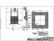
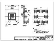
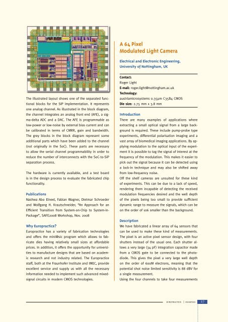
A 64 PixelModulated Light CameraElectrical and Electronic Engineering,University of Nottingham, UKThe illustrated layout shows one of the separated functionalblocks for the SiP implementation. It representsone analog channel. As illustrated in the block diagram,the channel integrates an analog front end (AFE), a sigma-deltaADC and a DAC. The AFE is programmable aslow-power or low-noise by external bias current and canbe calibrated in terms of CMRR, gain and bandwidth.The grey blocks in the block diagram represent someadditional parts which have been added to the channel(not originally in the SoC). These parts are necessaryto allow the serial channel programmability in order toreduce the number of interconnects with the SoC-to-SiPseparation process.The hardware is currently available, and a test boardis in the design process to evaluate the fabricated chipfunctionality.PublicationsNashwa Abo Elneel, Fabian Wagner, Dietmar Schroederand Wolfgang H. Krautschneider, “An Approach for anEfficient Transition from System-on-Chip to System-in-Package”, SAFE<strong>2008</strong> Workshop, Nov. <strong>2008</strong>Why <strong>Europractice</strong>?<strong>Europractice</strong> has a variety of fabrication technologiesand offers the mini@sic program which allows to fabricatedies having relatively small sizes at affordableprices. In addition, it offers the opportunity for universitiesto manufacture designs that are based on academicresearch and not industry related. The <strong>Europractice</strong>staff, both at the Fraunhofer Institute and IMEC, provideexcellent service and supply us with all the necessaryinformation needed to implement such advanced mixedsignalcircuits in modern CMOS technologies.Contact:Roger LightE-mail: roger.light@nottingham.ac.ukTechnology:austriamicrosystems 0.35µm C35B4 CMOSDie size: 2.75 mm x 3.8 mmIntroductionThere are many examples of applications whereextracting a small optical signal from a large backgroundis required. These include pump-probe typeexperiments, differential polarisation imaging and avast array of biomedical imaging applications. By applyingmodulation to the optical input of the experimentit is possible to tag the signal of interest at thefrequency of the modulation. This makes it easier topick out the signal because it can be detected usinga lock-in technique and may also be shifted awayfrom low-frequency noise.Off the shelf cameras are unsuited for these kindof experiments. This can be due to a lack of speed,rendering them incapable of detecting the receivedmodulation frequencies desired and the well depthof the pixels being too small to provide sufficientdynamic range to measure the signals, which can beon the order of 106 smaller than the background.DescriptionWe have fabricated a linear array of 64 sensors thatcan be used to make these kind of measurements.The pixel is an active pixel sensor design, with fourshutters instead of the usual one. Each shutter allowsa very large (34 pF) integration capacitor madefrom a CMOS gate to be connected to the photodiode.This gives the pixel a very large well depthon the order of 600M electrons, meaning that thepotential shot noise limited sensitivity is 88 dBV fora single measurement.Using the four channels to take four measurementseuropractice | examples27