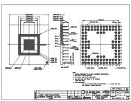
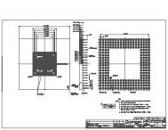
High-Frequency Integrated Power Supply on ChipDepartment of Electrical Engineering, University College Cork, IrelandContact:Jason Hannon, Raymond Foley, Kevin McCarthy, Michael EganEmail: raymond.foley@ucc.ieTechnology: AMS 0.35 μm C35B4 CMOSDie size: 3.6 mm x 2.3 mmThe design was created using theCadence DFWII framework and implementedon the AMS 0.35 μmprocess. This was chosen primarilydue to the particular voltage requirementsof the design, thoughdemonstration the design on a bulkCMOS process such as this was alsoan important objective.DescriptionIn recent years, increased miniaturisationand integration in electronicdevices has resulted in expandedfunctionality within shrinking formfactors,particularly in the mobile andhand-held space. From the power deliverypoint of view this has drivena demand for higher power supplydensity and efficiency. Switchingregulators can enable very high efficiency(compared to linear regulators),however the external passivecomponents (inductor and capacitors)they require have an excessivearea and volume overhead at today’stypical operating frequencies (3-8MHz). The aim of this research is todevelop switching regulator technologyoperating at up to 50 MHz inorder to reduce the size of the externalpassives whilst mitigating theeffects of increased switching lossthrough multiple operation modesand on-the-fly optimisation. The particulardesign iteration shown herewas used to explore the benefits ofdynamic switch sizing, load-scheduledfrequency scaling and optimalgate-drive timing parameters. Thedie includes a buck converter powertrain (composed of two independentparallel PMOS top devices and a singleNMOS bottom device), on-chipcapacitive decoupling, low-loss gatedrivecircuitry, a frequency-programmabledigital pulse-width modulator(20 MHz to 50 MHz) and a communication/controlinterface. Results fromthis prototype will be presented atthe Applied Power Electronics Conferencein February 2009.Why <strong>Europractice</strong>?University College Cork is an activemember of EUROPRACT<strong>IC</strong>E, andfabricates a number of <strong>IC</strong>s throughthis route annually. The frequentMPW runs, access to design toolsincluding the AMS HitKit and designsupport/advice makes the processvery attractive to a university-basedresearch group. Furthermore, thequick turn-around time from designfileto chip delivery has enabled usto produce multiple design revisionsin a short time-scale.20europractice | examples
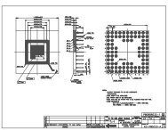
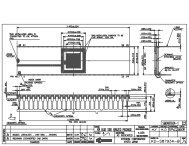
A Sub-μW Fully Tunable CMOS DPS for Uncooled Infrared Fast ImagingIntegrated Circuits and Systems Group, Instituto de Microelectrónica de Barcelona (IMB),Centro Nacional de Microelectrónica (CNM), Consejo Superior de Investigaciones Científicas (CS<strong>IC</strong>)SpainContact:Francesc Serra-GraellsE-mail: paco.serra@cnm.esTechnology: AMS 0.35μm CMOS C35B4C3Die size: 6.2 x 5.1 mm 2DescriptionThere is an increasing demand forinfrared (IR) fast digital imagers inkey application fields like automotive,medical, scientific and strategicequipments. In this sense, the pixelby-pixelcombination of PbSe detectors[1] and digital CMOS read-outcircuits, either by post-processing orbump-bonding, is a promising technologyfor low-cost, uncooled andvery fast (>100fps) IR imagers.This work presents a 32pixel x 32pixel focal plane array (FPA) of digitalactive pixel sensors (DPS) specificallydesigned for uncooled photoconductiveIR detectors. Each DPScell of 130μm x 130μm contains allthe CMOS circuits for input capacitanceand dark current compensation,A/D conversion, fixed patternnoise (FPN) cancellation, local biasgeneration and digital-only I/O communication.The inclusion of the A/D conversioninside each DPS eliminates the extracost of a high-speed serial A/D converter(ADC) at the output, and alsoit improves signal integrity by narrowingthe noise bandwidth throughthe massive A/D conversion of allthe pixels of the FPA working in parallel.The in-pixel predictive ADC involvesa pulse density modulator, incharge of quantifying in continuoustimethe amplitude of the sensorsignal at 1bit, and a digital counter,to cut off the high frequency componentsof the resulting quantificationnoise and to complete the timediscretization. This asynchronousspike-counting implementation exhibitslow switching activity duringacquisition, so less digital noise isinjected in the FPA. The self-bias capabilityof the DPS also minimizescross-talk between pixels comparedto the classical use of global analogbiasing schemes.The DPS can be operated in two differentmodes: acquisition or communication.In the first case, the inputblocks compensate for the sensorcapacitance and the DC dark currentI dark, so the effective signal I eff,ideally proportional to the incomingIR power, is codified by the spikecountingADC and stored in the digitalI/O block. During the communicationphase, the same digital blockis reconfigured to allow at the sametime both, the serial read-out of theIR sample, and the programminginof I darkand the gain of the ADCthrough V that alternate frames withoutextra speed costs. In fact, theindividual programmability of offsetand gain for each DPS allows notonly to fully cancel the pixel FPNdue to technology mismatching, butalso to apply both dynamic (i.e. ateach frame) and spatial (i.e. in differentregions of the FPA) automaticgain control (AGC) algorithms in orderto improve the dynamic range ofthe IR image.Thanks to the use of novel CMOScircuits [2] , which combine both subthrehsoldoperation and dynamicbiasing, a very low-power staticconsumption of 1000fps.The rest of features are: input compensationof capacitance up to 15pFand of dark current from 0.1μA to5μA; output signal dynamic rangeof 10bit from 1nA to 1μA; full digitaltuning capabilities against FPN, asshown in the experimental curvesof the figure; and built-in bias referencedeviations below 15%.europractice | examples21