YSM Issue 96.3

Create successful ePaper yourself
Turn your PDF publications into a flip-book with our unique Google optimized e-Paper software.
FOCUS<br />
Electrical Engineering<br />
WHY TINY PATTERNS MEAN BIG THINGS<br />
FOR THE FUTURE OF SEMICONDUCTORS<br />
BY WILLIAM ARCHACKI<br />
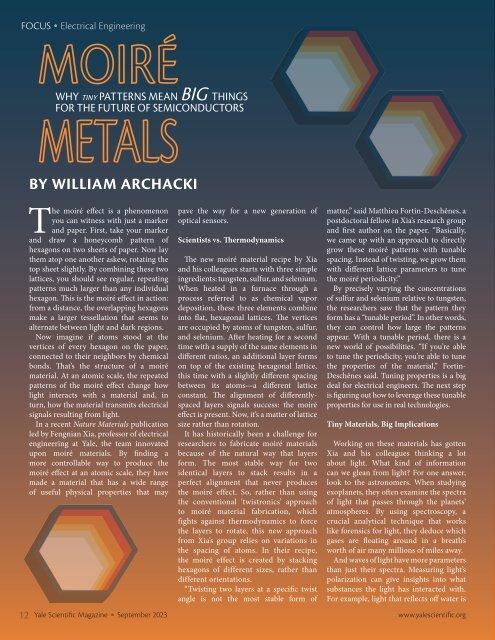
The moiré effect is a phenomenon<br />
you can witness with just a marker<br />
and paper. First, take your marker<br />
and draw a honeycomb pattern of<br />
hexagons on two sheets of paper. Now lay<br />
them atop one another askew, rotating the<br />
top sheet slightly. By combining these two<br />
lattices, you should see regular, repeating<br />
patterns much larger than any individual<br />
hexagon. This is the moiré effect in action:<br />
from a distance, the overlapping hexagons<br />
make a larger tessellation that seems to<br />
alternate between light and dark regions.<br />
Now imagine if atoms stood at the<br />
vertices of every hexagon on the paper,<br />
connected to their neighbors by chemical<br />
bonds. That’s the structure of a moiré<br />
material. At an atomic scale, the repeated<br />
patterns of the moiré effect change how<br />
light interacts with a material and, in<br />
turn, how the material transmits electrical<br />
signals resulting from light.<br />
In a recent Nature Materials publication<br />
led by Fengnian Xia, professor of electrical<br />
engineering at Yale, the team innovated<br />
upon moiré materials. By finding a<br />
more controllable way to produce the<br />
moiré effect at an atomic scale, they have<br />
made a material that has a wide range<br />
of useful physical properties that may<br />
pave the way for a new generation of<br />
optical sensors.<br />
Scientists vs. Thermodynamics<br />
The new moiré material recipe by Xia<br />
and his colleagues starts with three simple<br />
ingredients: tungsten, sulfur, and selenium.<br />
When heated in a furnace through a<br />
process referred to as chemical vapor<br />
deposition, these three elements combine<br />
into flat, hexagonal lattices. The vertices<br />
are occupied by atoms of tungsten, sulfur,<br />
and selenium. After heating for a second<br />
time with a supply of the same elements in<br />
different ratios, an additional layer forms<br />
on top of the existing hexagonal lattice,<br />
this time with a slightly different spacing<br />
between its atoms—a different lattice<br />
constant. The alignment of differentlyspaced<br />
layers signals success: the moiré<br />
effect is present. Now, it’s a matter of lattice<br />
size rather than rotation.<br />
It has historically been a challenge for<br />
researchers to fabricate moiré materials<br />
because of the natural way that layers<br />
form. The most stable way for two<br />
identical layers to stack results in a<br />
perfect alignment that never produces<br />
the moiré effect. So, rather than using<br />
the conventional ‘twistronics’ approach<br />
to moiré material fabrication, which<br />
fights against thermodynamics to force<br />
the layers to rotate, this new approach<br />
from Xia’s group relies on variations in<br />
the spacing of atoms. In their recipe,<br />
the moiré effect is created by stacking<br />
hexagons of different sizes, rather than<br />
different orientations.<br />
“Twisting two layers at a specific twist<br />
angle is not the most stable form of<br />
matter,” said Matthieu Fortin-Deschênes, a<br />
postdoctoral fellow in Xia’s research group<br />
and first author on the paper. “Basically,<br />
we came up with an approach to directly<br />
grow these moiré patterns with tunable<br />
spacing. Instead of twisting, we grow them<br />
with different lattice parameters to tune<br />
the moiré periodicity.”<br />
By precisely varying the concentrations<br />
of sulfur and selenium relative to tungsten,<br />
the researchers saw that the pattern they<br />
form has a “tunable period”. In other words,<br />
they can control how large the patterns<br />
appear. With a tunable period, there is a<br />
new world of possibilities. “If you’re able<br />
to tune the periodicity, you’re able to tune<br />
the properties of the material,” Fortin-<br />
Deschênes said. Tuning properties is a big<br />
deal for electrical engineers. The next step<br />
is figuring out how to leverage these tunable<br />
properties for use in real technologies.<br />
Tiny Materials, Big Implications<br />
Working on these materials has gotten<br />
Xia and his colleagues thinking a lot<br />
about light. What kind of information<br />
can we glean from light? For one answer,<br />
look to the astronomers. When studying<br />
exoplanets, they often examine the spectra<br />
of light that passes through the planets’<br />
atmospheres. By using spectroscopy, a<br />
crucial analytical technique that works<br />
like forensics for light, they deduce which<br />
gases are floating around in a breath’s<br />
worth of air many millions of miles away.<br />
And waves of light have more parameters<br />
than just their spectra. Measuring light’s<br />
polarization can give insights into what<br />
substances the light has interacted with.<br />
For example, light that reflects off water is<br />
12 Yale Scientific Magazine September 2023 www.yalescientific.org