The Role of Wafer Bonding in 3D Integration and ... - SUSS MicroTec
The Role of Wafer Bonding in 3D Integration and ... - SUSS MicroTec
The Role of Wafer Bonding in 3D Integration and ... - SUSS MicroTec

You also want an ePaper? Increase the reach of your titles
YUMPU automatically turns print PDFs into web optimized ePapers that Google loves.
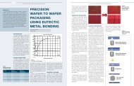
diffusion at temperatures as low as 200°C us<strong>in</strong>g a<br />
self-assembled monolayer approach or at room<br />
temperature after ion sputter clean<strong>in</strong>g.<br />
For Cu eutectic wafer bond<strong>in</strong>g, the surface<br />
micro-roughness is not as important. <strong>The</strong>re is<br />
significant <strong>in</strong>dustry experience from solder jo<strong>in</strong>t<br />
studies relat<strong>in</strong>g to chip packag<strong>in</strong>g that <strong>in</strong>dicates this<br />
bond approach is also less sensitive to surface<br />
contam<strong>in</strong>ation[4]. <strong>The</strong> lower process<strong>in</strong>g temperature<br />
also makes it friendlier for wafer process<strong>in</strong>g thermal<br />
budgets.<br />
Si<br />
Interface Cu<br />
Interface<br />
Cu<br />
Si<br />
1μm<br />
Fig. 2. Cu-Cu bond <strong>in</strong>terface show<strong>in</strong>g gra<strong>in</strong><br />
boundary.<br />
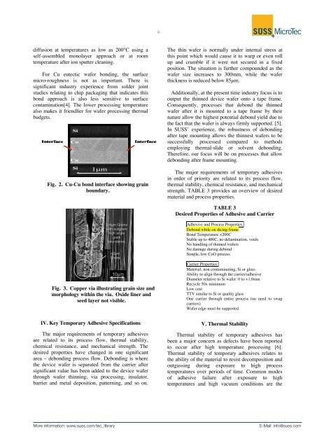
2-4µm Gra<strong>in</strong>s<br />
with subgra<strong>in</strong><br />
high angle<br />
gra<strong>in</strong><br />
boundaries.<br />