The Role of Wafer Bonding in 3D Integration and ... - SUSS MicroTec
The Role of Wafer Bonding in 3D Integration and ... - SUSS MicroTec
The Role of Wafer Bonding in 3D Integration and ... - SUSS MicroTec

You also want an ePaper? Increase the reach of your titles
YUMPU automatically turns print PDFs into web optimized ePapers that Google loves.
<strong>The</strong> key characteristics <strong>of</strong> the 3M process <strong>in</strong>clude<br />
room temperature debond<strong>in</strong>g <strong>and</strong> debond<strong>in</strong>g after<br />
frame mount<strong>in</strong>g.<br />
3M: Materials/Process<br />
Temporary Bond<br />
Device <strong>Wafer</strong><br />
Glass Carrier<br />
<strong>Wafer</strong><br />
Debond<br />
Th<strong>in</strong>ned Device<br />
<strong>Wafer</strong><br />
Carrier <strong>Wafer</strong><br />
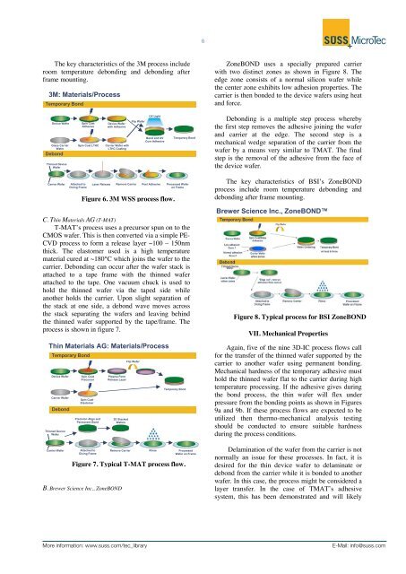
C. Th<strong>in</strong> Materials AG (T-MAT)<br />
T-MATʼs process uses a precursor spun on to the<br />
CMOS wafer. This is then converted via a simple PE-<br />
CVD process to form a release layer ~100 – 150nm<br />
thick. <strong>The</strong> elastomer used is a high temperature<br />
material cured at ~180°C which jo<strong>in</strong>s the wafer to the<br />
carrier. Debond<strong>in</strong>g can occur after the wafer stack is<br />
attached to a tape frame with the th<strong>in</strong>ned wafer<br />
attached to the tape. One vacuum chuck is used to<br />
hold the th<strong>in</strong>ned wafer via the taped side while<br />
another holds the carrier. Upon slight separation <strong>of</strong><br />
the stack at one side, a debond wave moves across<br />
the stack separat<strong>in</strong>g the wafers <strong>and</strong> leav<strong>in</strong>g beh<strong>in</strong>d<br />
the th<strong>in</strong>ned wafer supported by the tape/frame. <strong>The</strong><br />
process is shown <strong>in</strong> figure 7.<br />
Th<strong>in</strong> Materials AG: Materials/Process<br />
Temporary Bond<br />
Device <strong>Wafer</strong><br />
Carrier <strong>Wafer</strong><br />
Debond<br />
Th<strong>in</strong>ned Device<br />
<strong>Wafer</strong><br />
Attached to<br />
Dic<strong>in</strong>g Frame<br />
Sp<strong>in</strong> Coat<br />
Adhesive<br />
Sp<strong>in</strong> Coat LTHC<br />
Sp<strong>in</strong> Coat<br />
Precursor<br />
Sp<strong>in</strong> Coat<br />
Elastomer<br />
Precision Align <strong>and</strong><br />
Permanent Bond<br />
Carrier <strong>Wafer</strong> Attached to<br />
Dic<strong>in</strong>g Frame<br />
Device <strong>Wafer</strong><br />
with Adhesive<br />
Carrier <strong>Wafer</strong> with<br />
LTHC Coat<strong>in</strong>g<br />
Plasma Form<br />
Release Layer<br />
<strong>3D</strong> Stacked<br />
<strong>Wafer</strong>s<br />
Remove Carrier<br />
B. Brewer Science Inc., ZoneBOND<br />
Flip <strong>Wafer</strong><br />
Flip <strong>Wafer</strong><br />
UV Light<br />
Bond <strong>and</strong> UV<br />
Cure Adhesive<br />
Laser Release Remove Carrier Peel Adhesive<br />
Figure 6. 3M WSS process flow.<br />
R<strong>in</strong>se<br />
Temporary Bond<br />
Processed <strong>Wafer</strong><br />
on Frame<br />
Temporary Bond<br />
Figure 7. Typical T-MAT process flow.<br />
Processed<br />
<strong>Wafer</strong> on Frame<br />
6<br />
ZoneBOND uses a specially prepared carrier<br />
with two dist<strong>in</strong>ct zones as shown <strong>in</strong> Figure 8. <strong>The</strong><br />
edge zone consists <strong>of</strong> a normal silicon wafer while<br />
the center zone exhibits low adhesion properties. <strong>The</strong><br />
carrier is then bonded to the device wafers us<strong>in</strong>g heat<br />
<strong>and</strong> force.<br />
Debond<strong>in</strong>g is a multiple step process whereby<br />
the first step removes the adhesive jo<strong>in</strong><strong>in</strong>g the wafer<br />
<strong>and</strong> carrier at the edge. <strong>The</strong> second step is a<br />
mechanical wedge separation <strong>of</strong> the carrier from the<br />
wafer by a means very similar to TMAT. <strong>The</strong> f<strong>in</strong>al<br />
step is the removal <strong>of</strong> the adhesive from the face <strong>of</strong><br />
the device wafer.<br />
<strong>The</strong> key characteristics <strong>of</strong> BSIʼs ZoneBOND<br />
process <strong>in</strong>clude room temperature debond<strong>in</strong>g <strong>and</strong><br />
debond<strong>in</strong>g after frame mount<strong>in</strong>g.<br />
Brewer Science Inc., ZoneBOND<br />
Figure 8. Typical process for BSI ZoneBOND<br />
VII. Mechanical Properties<br />
Aga<strong>in</strong>, five <strong>of</strong> the n<strong>in</strong>e <strong>3D</strong>-IC process flows call<br />
for the transfer <strong>of</strong> the th<strong>in</strong>ned wafer supported by the<br />
carrier to another wafer us<strong>in</strong>g permanent bond<strong>in</strong>g.<br />
Mechanical hardness <strong>of</strong> the temporary adhesive must<br />
hold the th<strong>in</strong>ned wafer flat to the carrier dur<strong>in</strong>g high<br />
temperature process<strong>in</strong>g. If the adhesive gives dur<strong>in</strong>g<br />
the bond process, the th<strong>in</strong> wafer will flex under<br />
pressure from the bond<strong>in</strong>g po<strong>in</strong>ts as shown <strong>in</strong> Figures<br />
9a <strong>and</strong> 9b. If these process flows are expected to be<br />
utilized then thermo-mechanical analysis test<strong>in</strong>g<br />
should be conducted to ensure suitable hardness<br />
dur<strong>in</strong>g the process conditions.<br />
Delam<strong>in</strong>ation <strong>of</strong> the wafer from the carrier is not<br />
normally an issue for these processes. In fact, it is<br />
desired for the th<strong>in</strong> device wafer to delam<strong>in</strong>ate or<br />
debond from the carrier while it is bonded to another<br />
wafer. In this case, the process might be considered a<br />
layer transfer. In the case <strong>of</strong> TMATʼs adhesive<br />
system, this has been demonstrated <strong>and</strong> will likely<br />
More <strong>in</strong>formation: www.suss.com/tec_library E-Mail: <strong>in</strong>fo@suss.com