RH1021-5 - Precision 5V Reference - Linear Technology
RH1021-5 - Precision 5V Reference - Linear Technology
RH1021-5 - Precision 5V Reference - Linear Technology

Create successful ePaper yourself
Turn your PDF publications into a flip-book with our unique Google optimized e-Paper software.
DESCRIPTIO U<br />
The <strong>RH1021</strong>-5 is a precision <strong>5V</strong> reference with ultralow<br />
drift and noise, extremely good long term stability and<br />
almost total immunity to input voltage variations. The<br />
reference output will source and sink up to 10mA. Unique<br />
circuit design makes the <strong>RH1021</strong>-5 the first IC reference<br />
to offer ultralow drift without the use of high power onchip<br />
heaters.<br />
The wafer lots are processed to <strong>Linear</strong> <strong>Technology</strong>’s inhouse<br />
Class S flow to yield circuits usable in stringent<br />
military applications.<br />
, LTC and LT are registered trademarks of <strong>Linear</strong> <strong>Technology</strong> Corporation.<br />
All other trademarks are the property of their respective owners.<br />
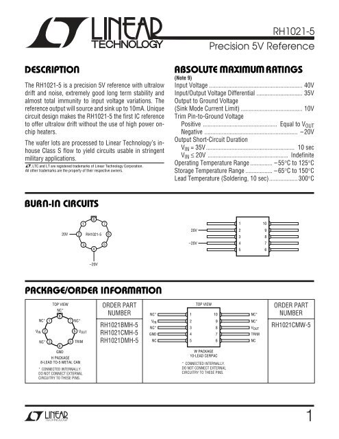
BUR -I CIRCUITS<br />
VIN<br />
NC*<br />
U<br />
2<br />
NC*<br />
1<br />
3<br />
U<br />
20V<br />
TOP VIEW<br />
NC*<br />
8<br />
4<br />
GND<br />
7<br />
5<br />
2<br />
NC*<br />
6<br />
1<br />
3<br />
V OUT<br />
TRIM<br />
H PACKAGE<br />
8-LEAD TO-5 METAL CAN<br />
* CONNECTED INTERNALLY.<br />
DO NOT CONNECT EXTERNAL<br />
CIRCUITRY TO THESE PINS.<br />
8<br />
<strong>RH1021</strong>-5<br />
4<br />
–20V<br />
U U W<br />
PACKAGE/ORDER I FOR ATIO<br />
7<br />
5<br />
6<br />
ORDER PART<br />
NUMBER<br />
<strong>RH1021</strong>BMH-5<br />
<strong>RH1021</strong>CMH-5<br />
<strong>RH1021</strong>DMH-5<br />
NC*<br />
V IN<br />
NC*<br />
GND<br />
NC<br />
<strong>RH1021</strong>-5<br />
<strong>Precision</strong> <strong>5V</strong> <strong>Reference</strong><br />
ABSOLUTE AXI U RATI GS<br />
W W W<br />
(Note 9)<br />
Input Voltage ........................................................... 40V<br />
Input/Output Voltage Differential ............................. 3<strong>5V</strong><br />
Output to Ground Voltage<br />
(Sink Mode Current Limit) ....................................... 10V<br />
Trim Pin-to-Ground Voltage<br />
Positive ............................................... Equal to V OUT<br />
Negative ........................................................... –20V<br />
Output Short-Circuit Duration<br />
V IN = 3<strong>5V</strong> ........................................................ 10 sec<br />
VIN ≤ 20V ................................................... Indefinite<br />
Operating Temperature Range .............. –55°C to 125°C<br />
Storage Temperature Range ................. – 65°C to 150°C<br />
Lead Temperature (Soldering, 10 sec).................. 300°C<br />
1<br />
2<br />
3<br />
4<br />
5<br />
20V<br />
–20V<br />
TOP VIEW<br />
10<br />
9<br />
8<br />
7<br />
6<br />
W PACKAGE<br />
10-LEAD CERPAC<br />
* CONNECTED INTERNALLY.<br />
DO NOT CONNECT EXTERNAL<br />
CIRCUITRY TO THESE PINS.<br />
1<br />
2<br />
3<br />
4<br />
5<br />
NC*<br />
NC*<br />
VOUT TRIM<br />
NC<br />
10<br />
9<br />
8<br />
7<br />
6<br />
U<br />
ORDER PART<br />
NUMBER<br />
<strong>RH1021</strong>CMW-5<br />
1
<strong>RH1021</strong>-5<br />
TABLE 1: ELECTRICAL CHARACTERISTICS<br />
TA = 25°C SUB- –55°C ≤ TA ≤ 125°C SUB-<br />
SYMBOL PARAMETER CONDITIONS NOTES MIN TYP MAX GROUP MIN TYP MAX GROUP UNITS<br />
V OUT Output Voltage <strong>RH1021</strong>CM-5 1 4.9975 5.0025 1 V<br />
<strong>RH1021</strong>BM-5, DM-5 1 4.95 5.05 1 V<br />
TCVOUT Output Voltage <strong>RH1021</strong>BM-5 2 5 2,3 ppm/°C<br />
Temperature Coefficient <strong>RH1021</strong>CM-5, DM-5 2 20 2,3 ppm/°C<br />
∆VOUT Line Regulation 7.2V ≤ VIN ≤ 10V 3 12 1 20 2,3 ppm/V<br />
∆V IN 10V ≤ V IN ≤ 40V 3 6 1 10 2,3 ppm/V<br />
∆VOUT Load Regulation 0 ≤ IOUT ≤ 10mA 3 20 1 35 2,3 ppm/mA<br />
∆IOUT (Sourcing Current)<br />
10Krad(Si) 20Krad(Si) 50Krad(Si) 100Krad(Si) 200Krad(Si)<br />
SYMBOL PARAMETER CONDITIONS NOTES MIN MAX MIN MAX MIN MAX MIN MAX MIN MAX UNITS<br />
V OUT Output Voltage <strong>RH1021</strong>CM-5 1 4.9945 5.0055 4.993 5.007 4.991 5.009 4.9875 5.0125 4.984 5.016 V<br />
<strong>RH1021</strong>BM-5, DM-5 1 4.95 5.05 4.945 5.055 4.942 5.058 4.94 5.06 4.935 5.065 V<br />
TCVOUT Output Voltage <strong>RH1021</strong>BM-5 2 5 5 5 7 10 ppm/°C<br />
Temperature Coefficient <strong>RH1021</strong>CM-5, DM-5 2 20 20 20 22 25 ppm/°C<br />
∆V OUT Line Regulation 7.2V ≤ V IN ≤ 10V 3 12 12 13.5 15 18 ppm/V<br />
∆V IN 10V ≤ V IN ≤ 40V 3 6 6 6 7 9 ppm/V<br />
∆VOUT Load Regulation 0 ≤ IOUT ≤ 10mA 3,7 20 20 20 20 20 ppm/mA<br />
∆IOUT (Sourcing Current)<br />
2<br />
(Preirradiation) (Note 8)<br />
Load Regulation 0 ≤ I OUT ≤ 10mA 3 100 1 150 2,3 ppm/mA<br />
(Sinking Current)<br />
I S Supply Current 1.2 1 1.5 2,3 mA<br />
Output Voltage Noise 0.1Hz ≤ f ≤ 10Hz 4 3 µV P-P<br />
10Hz ≤ f ≤ 1kHz 4 3.5 4 µV RMS<br />
Long Term Stability ∆T = 1000 Hrs 5 15 ppm<br />
of VOUT Noncumulative<br />
Temperature Hysteresis<br />
of VOUT<br />
∆T = ±25°C 10 ppm<br />
TABLE 1A: ELECTRICAL CHARACTERISTICS (Postirradiation) (Note 6)<br />
Load Regulation 0 ≤ I OUT ≤ 10mA 3 100 100 100 100 150 ppm/mA<br />
(Sinking Current)<br />
I S Supply Current 1.2 1.2 1.2 1.2 1.2 mA
TABLE 1A: ELECTRICAL CHARACTERISTICS (Postirradiation) (Note 6)<br />
Note 1: Output voltage is measured immediately after turn-on. Changes<br />
due to chip warm-up are typically less than 0.005%.<br />
Note 2: Temperature coefficient is measured by dividing the change in<br />
output voltage over the temperature range by the change in temperature.<br />
Separate tests are done for hot and cold; TMIN to 25°C and 25°C to T MAX.<br />
Incremental slope is also measured at 25°C.<br />
Note 3: Line and load regulation are measured on a pulse basis. Output<br />
changes due to die temperature change must be taken into account<br />
separately. Package thermal resistance is 150°C/W for the TO-5 (H)<br />
package and 170°C/W for the 10-lead flatpack (W) package.<br />
Note 4: RMS noise is measured with a 2-pole highpass filter at 10Hz and a<br />
2-pole lowpass filter at 1kHz. The resulting output is full wave rectified and<br />
then integrated for a fixed period, making the final reading an average as<br />
TABLE 2: ELECTRICAL TEST REQUIRE E TS<br />
MIL-STD-883 TEST REQUIREMENTS SUBGROUP<br />
Final Electrical Test Requirements (Method 5004) 1*,2,3,4<br />
Group A Test Requirements (Method 5005) 1,2,3,4<br />
Group B and D for Class S, and 1,2,3<br />
Group C and D for Class B<br />
End Point Electrical Parameters (Method 5005)<br />
* PDA Applies to subgroup 1. See PDA Test Notes.<br />
TOTAL DOSE BIAS CIRCUIT<br />
1<strong>5V</strong><br />
VIN<br />
GND<br />
–1<strong>5V</strong><br />
U W<br />
<strong>RH1021</strong>-5<br />
opposed to RMS. Correction factors are used to convert from average to<br />
RMS and to correct for the nonideal bandpass of the filters. Peak-to-peak<br />
noise is measured with a single highpass filter at 0.1Hz and a 2-pole<br />
lowpass filter at 10Hz. The unit is enclosed in a still-air environment to<br />
eliminate thermocouple effects on the leads. Test time is 10 seconds.<br />
Note 5: Consult factory for units with long term stability data.<br />
Note 6: VIN = 10V, I OUT = 0, T A = 25°C, unless otherwise noted.<br />
Note 7: I OUT(MAX) (Sourcing) is 5mA for exposures greater than 100Krad<br />
(Si).<br />
Note 8: VIN = 10V, I OUT = 0, unless otherwise noted.<br />
Note 9: Absolute Maximum Ratings are those values beyond which the life<br />
of a device may be impaired.<br />
PDA Test Notes<br />
The PDA is specified as 5% based on failures from group A, subgroup 1,<br />
tests after cooldown as the final electrical test in accordance with method<br />
5004 of MIL-STD-883. The verified failures of group A, subgroup 1, after<br />
burn-in divided by the total number of devices submitted for burn-in in<br />
that lot shall be used to determine the percent for the lot.<br />
<strong>Linear</strong> <strong>Technology</strong> Corporation reserves the right to test to tighter limits<br />
than those given.<br />
0.1µF<br />
Information furnished by <strong>Linear</strong> <strong>Technology</strong> Corporation is believed to be accurate and reliable.<br />
However, no responsibility is assumed for its use. <strong>Linear</strong> <strong>Technology</strong> Corporation makes no representation<br />
that the interconnection of its circuits as described herein will not infringe on existing patent rights.<br />
3
<strong>RH1021</strong>-5<br />
TYPICAL PERFOR A CE CHARACTERISTICS<br />
5.00<br />
OUTPUT VOLTAGE (V) 5.01<br />
4.99<br />
4<br />
Output Voltage<br />
1<br />
V IN = 10V<br />
IOUT = 0<br />
10 100 1000<br />
TOTAL DOSE Krad (Si)<br />
LINE REGULATION (ppm/V)<br />
10<br />
8<br />
6<br />
4<br />
2<br />
0<br />
–2<br />
1<br />
U W<br />
<strong>RH1021</strong>-5 G01<br />
Line Regulation<br />
LOAD REGULATION (ppm/mA)<br />
7.2V ≤ V IN ≤ 10V<br />
90<br />
80<br />
70<br />
60<br />
50<br />
40<br />
10V ≤ V IN ≤ 40V<br />
30<br />
1<br />
10 100 1000<br />
TOTAL DOSE Krad (Si)<br />
Load Regulation (Sinking)<br />
V IN = 10V<br />
0mA ≤ IOUT ≤ 10mA<br />
<strong>RH1021</strong>-5 G02<br />
<strong>Linear</strong> <strong>Technology</strong> Corporation<br />
1630 McCarthy Blvd., Milpitas, CA 95035-7417<br />
(408) 432-1900 ● FAX: (408) 434-0507 ● www.linear.com<br />
10 100 1000<br />
TOTAL DOSE Krad (Si)<br />
TEMPERATURE COEFFICIENT (ppm/°C)<br />
<strong>RH1021</strong>-5 G03<br />
15<br />
10<br />
5<br />
0<br />
–5<br />
–10<br />
–15<br />
1<br />
LOAD REGULATION (ppm/mA)<br />
V IN = 10V<br />
20<br />
18<br />
16<br />
14<br />
12<br />
10<br />
8<br />
6<br />
1<br />
Load Regulation (Sourcing)<br />
V IN = 10V<br />
0mA ≤ IOUT ≤ 10mA<br />
Temperature Coefficient<br />
10 100 1000<br />
TOTAL DOSE Krad (Si)<br />
NOTE 7<br />
10 100 1000<br />
TOTAL DOSE Krad (Si)<br />
<strong>RH1021</strong>-5 G04<br />
<strong>RH1021</strong>-5 G05<br />
I.D. No. 66-10-0177 Rev. E 1007<br />
LT 1007 REV E • PRINTED IN USA<br />
© LINEAR TECHNOLOGY CORPORATION 1990