LTC6945 - Ultralow Noise and Spurious 0.35GHz to 6GHz Integer-N ...
LTC6945 - Ultralow Noise and Spurious 0.35GHz to 6GHz Integer-N ...
LTC6945 - Ultralow Noise and Spurious 0.35GHz to 6GHz Integer-N ...

Create successful ePaper yourself
Turn your PDF publications into a flip-book with our unique Google optimized e-Paper software.
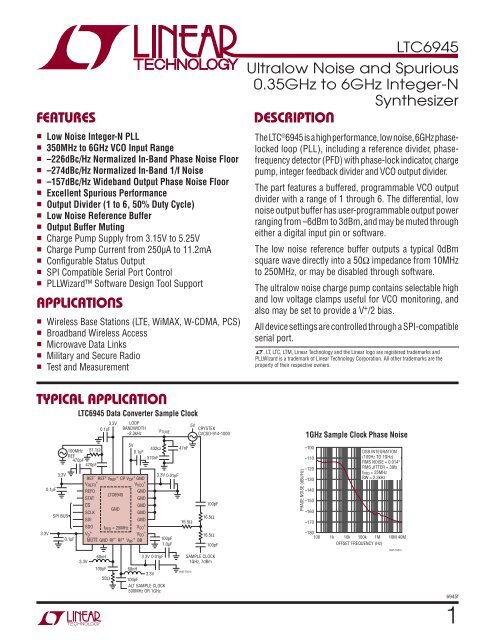
TYPICAL APPLICATION<br />
<strong>LTC6945</strong><br />
<strong>Ultralow</strong> <strong>Noise</strong> <strong>and</strong> <strong>Spurious</strong><br />
<strong>0.35GHz</strong> <strong>to</strong> <strong>6GHz</strong> <strong>Integer</strong>-N<br />
Synthesizer<br />
FEATURES DESCRIPTION<br />
n Low <strong>Noise</strong> <strong>Integer</strong>-N PLL<br />
n 350MHz <strong>to</strong> <strong>6GHz</strong> VCO Input Range<br />
n –226dBc/Hz Normalized In-B<strong>and</strong> Phase <strong>Noise</strong> Floor<br />
n –274dBc/Hz Normalized In-B<strong>and</strong> 1/f <strong>Noise</strong><br />
n –157dBc/Hz Wideb<strong>and</strong> Output Phase <strong>Noise</strong> Floor<br />
n Excellent <strong>Spurious</strong> Performance<br />
n Output Divider (1 <strong>to</strong> 6, 50% Duty Cycle)<br />
n Low <strong>Noise</strong> Reference Buffer<br />
n Output Buffer Muting<br />
n Charge Pump Supply from 3.15V <strong>to</strong> 5.25V<br />
n Charge Pump Current from 250μA <strong>to</strong> 11.2mA<br />
n Configurable Status Output<br />
n SPI Compatible Serial Port Control<br />
n PLLWizard Software Design Tool Support<br />
APPLICATIONS<br />
n Wireless Base Stations (LTE, WiMAX, W-CDMA, PCS)<br />
n Broadb<strong>and</strong> Wireless Access<br />
n Microwave Data Links<br />
n Military <strong>and</strong> Secure Radio<br />
n Test <strong>and</strong> Measurement<br />
3.3V<br />
0.1μF<br />
3.3V<br />
SPI BUS<br />
<strong>LTC6945</strong> Data Converter Sample Clock<br />
100MHz 51.1Ω<br />
REF<br />
470pF<br />
470pF<br />
0.1μF<br />
VVCO +<br />
VREFO +<br />
REF – REF + V<br />
+<br />
REF CP VCP<br />
+<br />
GND<br />
REFO<br />
STAT<br />
GND<br />
GND<br />
CS<br />
SCLK<br />
GND<br />
GND<br />
SDI<br />
GND<br />
SDO<br />
V<br />
+<br />
CO<br />
V<br />
+<br />
V<br />
–<br />
D CO<br />
MUTE GND RF –<br />
<strong>LTC6945</strong><br />
GND<br />
fPFD = 25MHz<br />
RF + VRF + BB<br />
3.3V<br />
3.3V<br />
0.1μF<br />
LOOP<br />
BANDWIDTH<br />
~2.3kHz<br />
5V<br />
432Ω<br />
0.1μF<br />
570nF<br />
VTUNE<br />
3.3V 0.01μF<br />
100pF<br />
1.0μF<br />
47nF<br />
16.5Ω<br />
68nH 3.3V 0.01μF SAMPLE CLOCK<br />
1GHz, 7dBm<br />
100pF<br />
50Ω<br />
68nH<br />
100pF<br />
3.3V<br />
6945 TA01b<br />
ALT SAMPLE CLOCK<br />
500MHz OR 1GHz<br />
5V<br />
CRYSTEK<br />
CVCSO-914-1000<br />
100pF<br />
16.5Ω<br />
16.5Ω<br />
100pF<br />
The LTC ® 6945 is a high performance, low noise, <strong>6GHz</strong> phaselocked<br />
loop (PLL), including a reference divider, phasefrequency<br />
detec<strong>to</strong>r (PFD) with phase-lock indica<strong>to</strong>r, charge<br />
pump, integer feedback divider <strong>and</strong> VCO output divider.<br />
The part features a buffered, programmable VCO output<br />
divider with a range of 1 through 6. The differential, low<br />
noise output buffer has user-programmable output power<br />
ranging from –6dBm <strong>to</strong> 3dBm, <strong>and</strong> may be muted through<br />
either a digital input pin or software.<br />
The low noise reference buffer outputs a typical 0dBm<br />
square wave directly in<strong>to</strong> a 50Ω impedance from 10MHz<br />
<strong>to</strong> 250MHz, or may be disabled through software.<br />
The ultralow noise charge pump contains selectable high<br />
<strong>and</strong> low voltage clamps useful for VCO moni<strong>to</strong>ring, <strong>and</strong><br />
also may be set <strong>to</strong> provide a V + /2 bias.<br />
All device settings are controlled through a SPI-compatible<br />
serial port.<br />
L, LT, LTC, LTM, Linear Technology <strong>and</strong> the Linear logo are registered trademarks <strong>and</strong><br />
PLLWizard is a trademark of Linear Technology Corporation. All other trademarks are the<br />
property of their respective owners.<br />
PHASE NOISE (dBc/Hz)<br />
1GHz Sample Clock Phase <strong>Noise</strong><br />
–100<br />
–110<br />
–120<br />
–130<br />
–140<br />
–150<br />
–160<br />
–170<br />
DSB INTEGRATION<br />
(100Hz TO 1GHz)<br />
RMS NOISE = 0.014°<br />
RMS JITTER = 39fs<br />
fPFD = 25MHz<br />
BW = 2.3kHz<br />
–180<br />
100 1k 10k 100k 1M 10M 40M<br />
OFFSET FREQUENCY (Hz)<br />
6945 TA01b<br />
6945f<br />
1
<strong>LTC6945</strong><br />
ABSOLUTE MAXIMUM RATINGS<br />
Supply Voltages<br />
V + (VREF + , VREFO + , VRF + , VVCO + , VD + ) <strong>to</strong> GND ......3.6V<br />
VCP + <strong>to</strong> GND .........................................................5.5V<br />
Voltage on CP Pin .................GND – 0.3V <strong>to</strong> VCP + + 0.3V<br />
Voltage on All Other Pins ..........GND – 0.3V <strong>to</strong> V + (Note 1)<br />
+ 0.3V<br />
Operating Case Temperature Range (TC)<br />
(Note 2) .................................................. –40°C <strong>to</strong> 105°C<br />
Operating Junction Temperature ........................... 125°C<br />
S<strong>to</strong>rage Temperature Range .................. –65°C <strong>to</strong> 150°C<br />
ORDER INFORMATION<br />
2<br />
PIN CONFIGURATION<br />
REF –<br />
REF +<br />
TOP VIEW<br />
VREF +<br />
CP<br />
VCP +<br />
GND<br />
28 27 26 25 24 23<br />
VREFO 1<br />
2<br />
3<br />
4 29<br />
5 GND<br />
6<br />
9 10 11 12 13 14<br />
+<br />
REFO<br />
STAT<br />
CS<br />
SCLK<br />
SDI<br />
SDO<br />
VD +<br />
V<br />
+<br />
VCO<br />
GND<br />
GND<br />
GND<br />
GND<br />
GND<br />
VCO +<br />
VCO –<br />
22<br />
21<br />
20<br />
19<br />
18<br />
17<br />
7<br />
16<br />
8 15<br />
MUTE<br />
GND<br />
RF –<br />
RF +<br />
V RF +<br />
BB<br />
UFD PACKAGE<br />
28-LEAD (4mm � 5mm) PLASTIC QFN<br />
T JMAX = 125°C, θ JC = 7°C/W<br />
EXPOSED PAD (PIN 29) IS GND, MUST BE SOLDERED TO PCB<br />
LEAD FREE FINISH TAPE AND REEL PART MARKING PACKAGE DESCRIPTION CASE TEMPERATURE RANGE<br />
<strong>LTC6945</strong>IUFD#PBF <strong>LTC6945</strong>IUFD#TRPBF 6945 28-Lead (4mm × 5mm) Plastic QFN –40°C <strong>to</strong> 105°C<br />
Consult LTC Marketing for parts specified with wider operating temperature ranges.<br />
Consult LTC Marketing for information on non-st<strong>and</strong>ard lead based finish parts.<br />
For more information on lead free part marking, go <strong>to</strong>: http://www.linear.com/leadfree/<br />
For more information on tape <strong>and</strong> reel specifications, go <strong>to</strong>: http://www.linear.com/tape<strong>and</strong>reel/<br />
ELECTRICAL CHARACTERISTICS<br />
The l denotes the specifications which apply over the full operating<br />
temperature range, otherwise specifications are at TC = 25°C. VREF + = VREF0 + = VD + = VRF + = VVCO + = 3.3V, VCP + = 5V unless otherwise<br />
specified. All voltages are with respect <strong>to</strong> GND.<br />
SYMBOL PARAMETER CONDITIONS MIN TYP MAX UNITS<br />
Reference Inputs (REF + , REF – )<br />
fREF Input Frequency l 10 250 MHz<br />
VREF Input Signal Level Single-Ended l 0.5 2 3.3 VP-P Input Slew Rate l 20 V/μs<br />
Input Duty Cycle 50 %<br />
Self-Bias Voltage l 1.65 1.85 2.25 V<br />
Input Resistance Differential l 6.2 8.4 11.6 kΩ<br />
Input Capacitance Differential 3 pF<br />
6945f
ELECTRICAL CHARACTERISTICS<br />
<strong>LTC6945</strong><br />
The l denotes the specifications which apply over the full operating<br />
temperature range, otherwise specifications are at TC = 25°C. V +<br />
REF = VREF0<br />
+ = VD<br />
+ = VRF<br />
+ = VVCO<br />
+ = 3.3V, VCP<br />
+ = 5V unless otherwise<br />
specified. All voltages are with respect <strong>to</strong> GND.<br />
SYMBOL PARAMETER CONDITIONS MIN TYP MAX UNITS<br />
Reference Output (REFO)<br />
fREFO Output Frequency l 10 250 MHz<br />
PREFO Output Power fREFO = 10MHz, RLOAD = 50Ω l –0.2 3.2 dBm<br />
Output Impedance, Disabled<br />
VCO Input (VCO<br />
800 Ω<br />
+ , VCO – )<br />
fVCO Input Frequency l 350 6000 MHz<br />
PVCOI Input Power Level RZ = 50Ω, Single-Ended l –8 0 6 dBm<br />
Input Resistance Single-Ended, Each Input l 97 121 145 Ω<br />
RF Output (RF + , RF – )<br />
fRF Output Frequency l 350 6000 MHz<br />
O Output Divider Range All <strong>Integer</strong>s Included l 1 6<br />
Output Duty Cycle 50 %<br />
Output Resistance Single-Ended, Each Output <strong>to</strong> VRF + l 111 136 159 Ω<br />
Output Common Mode Voltage l 2.4 VRF + V<br />
PRF(SE) Output Power, Single-Ended,<br />
fRF = 900MHz<br />
RFO[1:0] = 0, RZ = 50Ω, LC Match<br />
RFO[1:0] = 1, RZ = 50Ω, LC Match<br />
RFO[1:0] = 2, RZ = 50Ω, LC Match<br />
RFO[1:0] = 3, RZ = 50Ω, LC Match<br />
l<br />
l<br />
l<br />
l<br />
–9.7<br />
–6.8<br />
–3.9<br />
–1.2<br />
–6.0<br />
–3.6<br />
–0.4<br />
2.3<br />
dBm<br />
dBm<br />
dBm<br />
dBm<br />
Output Power, Muted RZ = 50Ω, Single-Ended, fRF = 900MHz, O = 2 <strong>to</strong> 6 l –60 dBm<br />
Mute Enable Time l 110 ns<br />
Mute Disable Time l 170 ns<br />
Phase/Frequency Detec<strong>to</strong>r<br />
fPFD Input Frequency l 100 MHz<br />
Lock Indica<strong>to</strong>r, Available on the STAT Pin <strong>and</strong> via the SPI-Accessible Status Register<br />
tLWW Lock Window Width LKWIN[1:0] = 0<br />
3.0<br />
ns<br />
LKWIN[1:0] = 1<br />
10.0<br />
ns<br />
LKWIN[1:0] = 2<br />
30.0<br />
ns<br />
LKWIN[1:0] = 3<br />
90.0<br />
ns<br />
tLWHYS Charge Pump<br />
Lock Window Hysteresis Increase in tLWW Moving from Locked State <strong>to</strong><br />
Unlocked State<br />
22 %<br />
ICP Output Current Range 12 Settings (See Table 5) 0.25 11.2 mA<br />
Output Current Source/Sink Accuracy VCP = VCP + /2, All Settings ±6 %<br />
Output Current Source/Sink Matching ICP = 250μA <strong>to</strong> 1.4mA, VCP = V +<br />
CP /2<br />
ICP = 2mA <strong>to</strong> 11.2mA, VCP = V +<br />
CP /2<br />
±3.5<br />
±2<br />
%<br />
%<br />
Output Current vs Output Voltage<br />
Sensitivity<br />
(Note 3) l 0.1 0.5 %/V<br />
Output Current vs Temperature VCP = V +<br />
CP /2 l 170 ppm/°C<br />
Output Hi-Z Leakage Current ICP = 700μA, CPCLO = CPCHI = 0 (Note 3)<br />
ICP = 11.2mA, CPCLO = CPCHI = 0 (Note 3)<br />
0.5<br />
5<br />
nA<br />
nA<br />
VCLMP(LO) Low Clamp Voltage CPCLO = 1 0.84 V<br />
VCLMP(HI) High Clamp Voltage CPCHI = 1, Referred <strong>to</strong> VCP + –0.96 V<br />
VMID Mid-Supply Output Bias Ratio Referred <strong>to</strong> (VCP + – GND) 0.48 V/V<br />
6945f<br />
3
<strong>LTC6945</strong><br />
ELECTRICAL CHARACTERISTICS<br />
The l denotes the specifications which apply over the full operating<br />
temperature range, otherwise specifications are at TC = 25°C. V +<br />
REF = VREF0<br />
+ = VD<br />
+ = VRF<br />
+ = VVCO<br />
+ = 3.3V, VCP<br />
+ = 5V unless otherwise<br />
specified. All voltages are with respect <strong>to</strong> GND.<br />
SYMBOL PARAMETER CONDITIONS MIN TYP MAX UNITS<br />
Reference (R) Divider<br />
R Divide Range All <strong>Integer</strong>s Included l 1 1023 Counts<br />
VCO (N) Divider<br />
N Divide Range All <strong>Integer</strong>s Included l 32 65535 Counts<br />
Digital Pin Specifications<br />
VIH High Level Input Voltage MUTE, CS, SDI, SCLK l 1.55 V<br />
VIL Low Level Input Voltage MUTE, CS, SDI, SCLK l 0.8 V<br />
VIHYS Input Voltage Hysteresis MUTE, CS, SDI, SCLK 250 mV<br />
Input Current MUTE, CS, SDI, SCLK l ±1 μA<br />
IOH High Level Output Current SDO <strong>and</strong> STAT, VOH = V +<br />
D – 400mV l 1.4 2.3 mA<br />
IOL Low Level Output Current SDO <strong>and</strong> STAT, VOL = 400mV l 1.8 3.4 mA<br />
SDO Hi-Z Current<br />
Digital Timing Specifications (See Figures 8 <strong>and</strong> 9)<br />
l ±1 μA<br />
tCKH SCLK High Time l 25 ns<br />
tCKL SCLK Low Time l 25 ns<br />
tCSS CS Setup Time l 10 ns<br />
tCSH CS High Time l 10 ns<br />
tCS SDI <strong>to</strong> SCLK Setup Time l 6 ns<br />
tCH SDI <strong>to</strong> SCLK Hold Time l 6 ns<br />
tDO SCLK <strong>to</strong> SDO Time To VIH/VIL/Hi-Z with 30pF Load l 16 ns<br />
Power Supply Voltages<br />
V +<br />
REF Supply Range l 3.15 3.3 3.45 V<br />
V +<br />
REFO Supply Range l 3.15 3.3 3.45 V<br />
V +<br />
D Supply Range l 3.15 3.3 3.45 V<br />
V +<br />
RF Supply Range l 3.15 3.3 3.45 V<br />
V +<br />
VCO Supply Range l 3.15 3.3 3.45 V<br />
V +<br />
CP Supply Range<br />
Power Supply Currents<br />
l 3.15 5.25 V<br />
IDD V +<br />
D Supply Current Digital Inputs at Supply Levels l 250 μA<br />
ICC(CP) VCP + Supply Current ICP = 11.2mA<br />
ICP = 1.0mA<br />
PDALL = 1<br />
l<br />
l<br />
l<br />
33<br />
11<br />
235<br />
37<br />
12.3<br />
385<br />
mA<br />
mA<br />
μA<br />
ICC(REFO) V +<br />
REFO Supply Currents REFO Enabled, RZ = ∞ l 7.8 9.0 mA<br />
ICC Sum V +<br />
REF , VRF<br />
+ , VVCO<br />
+ Supply<br />
Currents<br />
RF Muted, OD[2:0] = 1<br />
RF Enabled, RFO[1:0] =0, OD[2:0] = 1<br />
l<br />
l<br />
68<br />
78<br />
75<br />
85<br />
mA<br />
mA<br />
RF Enabled, RFO[1:0] = 3, OD[2:0] = 1<br />
l<br />
87 95 mA<br />
RF Enabled, RFO[1:0] =3, OD[2:0] = 2<br />
l<br />
104 114 mA<br />
RF Enabled, RFO[1:0] =3, OD[2:0] = 3<br />
l<br />
110 121 mA<br />
RF Enabled, RFO[1:0] =3, OD[2:0] = 4 <strong>to</strong> 6 l<br />
115 125 mA<br />
PDALL = 1<br />
l<br />
202 396 μA<br />
4<br />
6945f
ELECTRICAL CHARACTERISTICS<br />
<strong>LTC6945</strong><br />
The l denotes the specifications which apply over the full operating<br />
temperature range, otherwise specifications are at TC = 25°C. V +<br />
REF = VREF0<br />
+ = VD<br />
+ = VRF<br />
+ = VVCO<br />
+ = 3.3V, VCP<br />
+ = 5V unless otherwise<br />
specified. All voltages are with respect <strong>to</strong> GND.<br />
SYMBOL PARAMETER CONDITIONS MIN TYP MAX UNITS<br />
Phase <strong>Noise</strong> <strong>and</strong> <strong>Spurious</strong><br />
LM(MIN) Output Phase <strong>Noise</strong> Floor (Note 5) RFO[1:0] = 3, OD[2:0] = 1, fRF = <strong>6GHz</strong><br />
RFO[1:0] = 3, OD[2:0] = 2, fRF = 3GHz<br />
RFO[1:0] = 3, OD[2:0] = 3, fRF = 2GHz<br />
RFO[1:0] = 3, OD[2:0] = 4, fRF = 1.5GHz<br />
RFO[1:0] = 3, OD[2:0] = 5, fRF = 1.2GHz<br />
RFO[1:0] = 3, OD[2:0] = 6, fRF = 1.0GHz<br />
–155<br />
–155<br />
–156<br />
–156<br />
–157<br />
–158<br />
dBc/Hz<br />
dBc/Hz<br />
dBc/Hz<br />
dBc/Hz<br />
dBc/Hz<br />
dBc/Hz<br />
LM(NORM) Normalized In-B<strong>and</strong> Phase <strong>Noise</strong> Floor ICP = 11.2mA (Notes 6, 7, 8) –226 dBc/Hz<br />
LM(NORM –1/f) Normalized In-B<strong>and</strong> 1/f Phase <strong>Noise</strong> ICP = 11.2mA (Notes 6, 9) –274 dBc/Hz<br />
LM(IB) In-B<strong>and</strong> Phase <strong>Noise</strong> Floor (Notes 6, 7, 8, 10) –99 dBc/Hz<br />
Integrated Phase <strong>Noise</strong> from 100Hz <strong>to</strong><br />
40MHz<br />
(Notes 4, 7, 10) 0.13 °RMS<br />
<strong>Spurious</strong> Reference Spur, PLL locked (Notes 4, 7, 10, 11) –102 dBc<br />
Note 1: Stresses beyond those listed under Absolute Maximum Ratings<br />
may cause permanent damage <strong>to</strong> the device. Exposure <strong>to</strong> any Absolute<br />
Maximum Rating condition for extended periods may affect device<br />
reliability <strong>and</strong> lifetime.<br />
Note 2: The <strong>LTC6945</strong>I is guaranteed <strong>to</strong> meet the specified performance<br />
limits over the –40°C <strong>to</strong> 105°C case temperature range.<br />
Note 3: For 0.8V ≤ VCP ≤ (V +<br />
CP – 0.8V).<br />
Note 4: VCO is Crystek CVCO55CL-0902-0928.<br />
Note 5: fVCO = <strong>6GHz</strong>, fOFFSET = 40MHz.<br />
Note 6: Measured inside the loop b<strong>and</strong>width with the loop locked.<br />
TYPICAL PERFORMANCE CHARACTERISTICS<br />
SENSITIVITY (dBm)<br />
–15<br />
–20<br />
–25<br />
–30<br />
–35<br />
–40<br />
–45<br />
–50<br />
–55<br />
0<br />
Note 7: Reference frequency supplied by Wenzel 501-04608A,<br />
fREF = 10MHz, P REF = 13dBm.<br />
Note 8: Output phase noise floor is calculated from normalized phase<br />
noise floor by LM(OUT) = –226 + 10log 10(f PFD) + 20log 10(f RF/f PFD).<br />
Note 9: Output 1/f phase noise is calculated from normalized 1/f phase<br />
noise by L M(OUT –1/f) = –274 + 20log 10 (f RF) – 10log 10 (f OFFSET).<br />
Note 10: I CP = 11.2mA, f PFD = 250kHz, f RF = 914MHz, FILT[1:0] = 3, Loop<br />
BW = 7kHz.<br />
Note 11: Measured using DC1649A.<br />
REF Input Sensitivity vs<br />
Frequency REFO Output Power vs Frequency REFO Phase <strong>Noise</strong><br />
BST = 1<br />
FILT = 0<br />
105°C<br />
25°C<br />
–40°C<br />
25 50 75 100 125 150 175 200 225 250<br />
FREQUENCY (MHz)<br />
6945 G01<br />
POUT (dBm)<br />
4<br />
3<br />
2<br />
1<br />
0<br />
–1<br />
–2<br />
–3<br />
–4<br />
0<br />
25 50 75 100 125 150 175 200 225 250<br />
FREQUENCY (MHz)<br />
105°C<br />
25°C<br />
–40°C<br />
6945 G02<br />
PHASE NOISE (dBc/Hz)<br />
–140<br />
–145<br />
–150<br />
–155<br />
P OUT = 1.45dBm<br />
fREF = 10MHz<br />
BST = 1<br />
FILT = 3<br />
NOTE 7<br />
–160<br />
100 1k 10k 100k 1M 5M<br />
OFFSET FREQUENCY (Hz)<br />
6945 G03<br />
6945f<br />
5
<strong>LTC6945</strong><br />
TYPICAL PERFORMANCE CHARACTERISTICS<br />
ERROR (%)<br />
ERROR (%)<br />
HD3 (dBc)<br />
6<br />
5<br />
4<br />
3<br />
2<br />
1<br />
0<br />
–1<br />
–2<br />
Charge Pump Sink Current Error<br />
vs Voltage, Output Current<br />
–3<br />
250μA<br />
–4<br />
1mA<br />
11.2mA<br />
–5<br />
0 0.5 1 1.5 2 2.5 3 3.5 4 4.5 5<br />
OUTPUT VOLTAGE (V)<br />
5<br />
4<br />
3<br />
2<br />
1<br />
0<br />
–1<br />
Charge Pump Source Current<br />
Error vs Voltage, Temperature<br />
RF Output HD3 vs Output Divide<br />
(Single-Ended On RF – )<br />
6945 G04<br />
–2<br />
–3<br />
ICP = 11.2mA<br />
–40°C<br />
–4 25°C<br />
105°C<br />
–5<br />
0 0.5 1 1.5 2 2.5 3 3.5 4 4.5 5<br />
OUTPUT VOLTAGE (V)<br />
–5<br />
–10<br />
–15<br />
–20<br />
O = 1<br />
f VCO (GHz)<br />
O = 2<br />
O = 6<br />
6945 G07<br />
O = 3<br />
fRF = fVCO/O –25 PVCO = 0dBm<br />
LC = 180nH<br />
CS = 270pF<br />
–30<br />
0 0.5 1 1.5 2 2.5 3 3.5 4 4.5 5 5.5 6<br />
6945 G10<br />
ERROR (%)<br />
P OUT (dBm)<br />
POUT AT f VCO/O (dBm)<br />
5<br />
4<br />
3<br />
2<br />
1<br />
0<br />
–1<br />
Charge Pump Sink Current Error<br />
vs Voltage, Temperature<br />
–2<br />
–3<br />
ICP = 11.2mA<br />
105°C<br />
–4<br />
25°C<br />
–40°C<br />
–5<br />
0 0.5 1 1.5 2 2.5 3 3.5 4 4.5 5<br />
OUTPUT VOLTAGE (V)<br />
1.0<br />
0.5<br />
0<br />
–0.5<br />
–1.0<br />
–1.5<br />
RF Output Power vs Frequency<br />
(Single-Ended On RF – )<br />
6945 G05<br />
–2.0<br />
–2.5<br />
PVCO = 0dBm<br />
LC = 180nH<br />
CS = 270pF<br />
105°C<br />
–3.0 25°C<br />
–3.5<br />
–40°C<br />
0 0.5 1 1.5 2 2.5 3 3.5 4 4.5 5 5.5 6<br />
FREQUENCY (GHz)<br />
–30<br />
–40<br />
–50<br />
–60<br />
–70<br />
–80<br />
–90<br />
–100<br />
–110<br />
6945 G08<br />
Charge Pump Source Current<br />
Error vs Voltage, Output Current<br />
–3<br />
250μA<br />
–4 1mA<br />
11.2mA<br />
–5<br />
0 0.5 1 1.5 2 2.5 3 3.5 4 4.5 5<br />
OUTPUT VOLTAGE (V)<br />
RF Output HD2 vs Output Divide<br />
(Single-Ended On RF – )<br />
MUTE Output Power<br />
vs f VCO <strong>and</strong> Output Divide<br />
(Single-Ended On RF – ) Frequency Step Transient<br />
f RF = f VCO/O<br />
PVCO = 0dBm<br />
LC = 180nH<br />
CS = 270pF<br />
O = 2<br />
O = 3<br />
O = 5<br />
O = 1<br />
O = 4<br />
O = 6<br />
–120<br />
0 0.5 1 1.5 2 2.5 3 3.5 4 4.5 5 5.5 6<br />
fVCO (GHz)<br />
6945 G11<br />
ERROR (%)<br />
HD2 (dBc)<br />
FREQUENCY (GHz)<br />
5<br />
4<br />
3<br />
2<br />
1<br />
0<br />
–1<br />
–2<br />
–20<br />
–25<br />
–30<br />
–35<br />
–40<br />
–45<br />
–50<br />
2.10<br />
2.05<br />
2.00<br />
1.95<br />
1.90<br />
1.85<br />
0<br />
f RF = f VCO/O<br />
PVCO = 0dBm<br />
LC = 180nH<br />
CS = 270pF<br />
O = 2<br />
O = 3<br />
O = 6<br />
O = 4<br />
6945 G06<br />
O = 5<br />
O = 1<br />
–55<br />
0 0.5 1 1.5 2 2.5 3 3.5 4 4.5 5 5.5 6<br />
fVCO (GHz)<br />
6945 G09<br />
f PFD = 1MHz<br />
BW = 40kHz<br />
100MHz STEP<br />
5 10 15 20 25 30 35 40 45<br />
TIME (μs)<br />
6945 G12<br />
6945f
TYPICAL PERFORMANCE CHARACTERISTICS<br />
SENSITIVITY (dBm)<br />
–10<br />
–15<br />
–20<br />
–25<br />
VCO Input Sensitivity<br />
vs Frequency, Temperature<br />
–30<br />
105°C<br />
25°C<br />
–35<br />
–40°C<br />
0 0.5 1 1.5 2 2.5 3 3.5 4 4.5 5 5.5 6<br />
FREQUENCY (GHz)<br />
P OUT (dBm)<br />
P OUT (dBm)<br />
0<br />
–20<br />
–40<br />
–60<br />
–80<br />
–100<br />
–120<br />
0<br />
–20<br />
–40<br />
–60<br />
–80<br />
–100<br />
–120<br />
6945 G13<br />
<strong>Spurious</strong> Response<br />
f RF = 914MHz, f REF = 10MHz,<br />
f PFD = 250kHz, Loop BW = 7kHz<br />
RBW = 1Hz<br />
VBW = 1Hz<br />
NOTES 7, 10, 11<br />
–113dBc –111dBc<br />
–140<br />
–10 –0.75 –0.5 –0.25 0 0.25 0.5 0.75 10<br />
FREQUENCY OFFSET (MHz, IN 10kHz SEGMENTS)<br />
Closed-Loop Phase <strong>Noise</strong>,<br />
f RF = 914MHz<br />
<strong>Spurious</strong> Response<br />
f RF = 2100MHz, f REF = 10MHz,<br />
f PFD = 1MHz, Loop BW = 40kHz<br />
<strong>Spurious</strong> Response<br />
f RF = 5725MHz, f REF = 10MHz,<br />
f PFD = 5MHz, Loop BW = 21kHz Supply Current vs Temperature<br />
RBW = 1Hz<br />
VBW = 1Hz<br />
NOTES 7, 11<br />
PHASE, NOISE (dBc/Hz)<br />
–102dBc –102dBc<br />
–100dBc –101dBc<br />
–90<br />
–100<br />
–110<br />
–120<br />
–130<br />
6945 G16<br />
–112dBc –112dBc<br />
–140<br />
–20 –15 –10 –5 0 5 10 15 20<br />
FREQUENCY OFFSET (MHz, IN 10kHz SEGMENTS)<br />
–140<br />
RMS NOISE = 0.13°<br />
–150<br />
fPFD = 250kHz<br />
BW = 7kHz<br />
–160<br />
NOTES 7, 10<br />
VCO = CRYSTEK<br />
CVCO55CL-0902-0928<br />
–170<br />
100 1k 10k 100k 1M 10M 40M<br />
OFFSET FREQUENCY (Hz)<br />
6945 G18<br />
P OUT (dBm)<br />
3.3V CURRENT (mA)<br />
0<br />
–20<br />
–40<br />
–60<br />
–80<br />
–100<br />
–120<br />
RBW = 1Hz<br />
VBW = 1Hz<br />
NOTES 7, 11<br />
–102dBc –102dBc<br />
<strong>LTC6945</strong><br />
Closed-Loop Phase <strong>Noise</strong>,<br />
f RF = 2100MHz<br />
–113dBc –112dBc<br />
–140<br />
–10 –3 –2 –1 0 1 2 3 10<br />
FREQUENCY OFFSET (MHz, IN 10kHz SEGMENTS)<br />
88<br />
87<br />
86<br />
85<br />
84<br />
83<br />
82<br />
81<br />
80<br />
–40<br />
6945 G14<br />
PDREFO = 1<br />
O = 1<br />
RFO = 3<br />
MUTE = 0<br />
ICP = 11.2mA<br />
PHASE, NOISE (dBc/Hz)<br />
–90<br />
–100<br />
–110<br />
–120<br />
–130<br />
–140<br />
RMS NOISE = 0.33°<br />
–150<br />
fPFD = 1MHz<br />
BW = 40kHz<br />
–160<br />
NOTE 7<br />
VCO = RFMD<br />
UMX-586-D16-G<br />
–170<br />
100 1k 10k 100k 1M 10M 40M<br />
OFFSET FREQUENCY (Hz)<br />
6945 G17<br />
31.5<br />
–20 0 20 40 60 80 100<br />
TEMPERATURE (°C)<br />
6945 G19<br />
35.5<br />
35.0<br />
34.5<br />
34.0<br />
33.5<br />
33.0<br />
32.5<br />
32.0<br />
5V CURRENT (mA)<br />
6945 G15<br />
6945f<br />
7
<strong>LTC6945</strong><br />
PIN FUNCTIONS<br />
VREFO + (Pin 1): 3.15V <strong>to</strong> 3.45V Positive Supply Pin for<br />
REFO Circuitry. This pin should be bypassed directly <strong>to</strong><br />
the ground plane using a 0.1μF ceramic capaci<strong>to</strong>r as close<br />
<strong>to</strong> the pin as possible.<br />
REFO (Pin 2): Reference Frequency Output. This produces<br />
a low noise square wave, buffered from the REF ± differential<br />
inputs. The output is self-biased <strong>and</strong> must be AC-coupled<br />
with a 22nF capaci<strong>to</strong>r.<br />
STAT (Pin 3): Status Output. This signal is a configurable<br />
logical OR combination of the UNLOK, LOK, THI <strong>and</strong> TLO<br />
status bits, programmable via the STATUS register. See<br />
the Operations section for more details.<br />
CS (Pin 4): Serial Port Chip Select. This CMOS input initiates<br />
a serial port communication burst when driven low,<br />
ending the burst when driven back high. See the Operations<br />
section for more details.<br />
SCLK (Pin 5): Serial Port Clock. This CMOS input clocks<br />
serial port input data on its rising edge. See the Operations<br />
section for more details.<br />
SDI (Pin 6): Serial Port Data Input. The serial port uses<br />
this CMOS input for data. See the Operations section for<br />
more details.<br />
SDO (Pin 7): Serial Port Data Output. This CMOS threestate<br />
output presents data from the serial port during a<br />
read communication burst. Optionally attach a resis<strong>to</strong>r<br />
of >200k <strong>to</strong> GND <strong>to</strong> prevent a floating output. See the<br />
Operations section for more details.<br />
VD + (Pin 8): 3.15V <strong>to</strong> 3.45V Positive Supply Pin for Serial<br />
Port Circuitry. This pin should be bypassed directly <strong>to</strong> the<br />
ground plane using a 0.1μF ceramic capaci<strong>to</strong>r as close <strong>to</strong><br />
the pin as possible.<br />
MUTE (Pin 9): RF Mute. The CMOS active-low input mutes<br />
the RF ± differential outputs while maintaining internal bias<br />
levels for quick response <strong>to</strong> de-assertion.<br />
GND (Pins 10, 17, 18, 19, 20, 21): Negative Power Supply<br />
(Ground). These pins should be tied directly <strong>to</strong> the ground<br />
plane with multiple vias for each pin.<br />
8<br />
RF – , RF + (Pins 11, 12): RF Output Signals. The VCO<br />
output divider is buffered <strong>and</strong> presented differentially on<br />
these pins. The outputs are open collec<strong>to</strong>r, with 136Ω<br />
(typical) pull-up resis<strong>to</strong>rs tied <strong>to</strong> VRF + <strong>to</strong> aid impedance<br />
matching. If used single-ended, the unused output should<br />
be terminated <strong>to</strong> 50Ω. See the Applications Information<br />
section for more details on impedance matching.<br />
VRF + (Pin 13): 3.15V <strong>to</strong> 3.45V Positive Supply Pin for<br />
RF Circuitry. This pin should be bypassed directly <strong>to</strong> the<br />
ground plane using a 0.01μF ceramic capaci<strong>to</strong>r as close<br />
<strong>to</strong> the pin as possible.<br />
BB (Pin 14): RF Reference Bypass. This output must be<br />
bypassed with a 1.0μF ceramic capaci<strong>to</strong>r <strong>to</strong> GND. Do not<br />
couple this pin <strong>to</strong> any other signal.<br />
VCO – , VCO + (Pins 15, 16): VCO Input Signals. The differential<br />
signal placed on these pins is buffered with a low<br />
noise amplifier <strong>and</strong> fed <strong>to</strong> the internal output <strong>and</strong> feedback<br />
dividers. These self-biased inputs must be AC-coupled<br />
<strong>and</strong> present a single-ended 121Ω (typical) resistance<br />
<strong>to</strong> aid impedance matching. They may be used singleended<br />
by bypassing VCO – <strong>to</strong> GND with a capaci<strong>to</strong>r. See<br />
the Applications Information section for more details on<br />
impedance matching.<br />
VVCO + (Pin 22): 3.15V <strong>to</strong> 3.45V Positive Supply Pin for<br />
VCO Circuitry. This pin should be bypassed directly <strong>to</strong> the<br />
ground plane using a 0.01μF ceramic capaci<strong>to</strong>r as close<br />
<strong>to</strong> the pin as possible.<br />
GND (23): Negative Power Supply (Ground). This pin is<br />
attached directly <strong>to</strong> the die attach paddle (DAP) <strong>and</strong> should<br />
be tied directly <strong>to</strong> the ground plane.<br />
VCP + (Pin 24): 3.15V <strong>to</strong> 5.25V Positive Supply Pin for Charge<br />
Pump Circuitry. This pin should be bypassed directly <strong>to</strong><br />
the ground plane using a 0.1μF ceramic capaci<strong>to</strong>r as close<br />
<strong>to</strong> the pin as possible.<br />
CP (Pin 25): Charge Pump Output. This bi-directional current<br />
output is normally connected <strong>to</strong> the external loop filter.<br />
See the Applications Information section for more details.<br />
6945f
PIN FUNCTIONS<br />
VREF + (Pin 26): 3.15V <strong>to</strong> 3.45V Positive Supply Pin for<br />
Reference Input Circuitry. This pin should be bypassed<br />
directly <strong>to</strong> the ground plane using a 0.1μF ceramic capaci<strong>to</strong>r<br />
as close <strong>to</strong> the pin as possible.<br />
REF + , REF – (Pins 27, 28): Reference Input Signals. This<br />
differential input is buffered with a low noise amplifier,<br />
which feeds the reference divider <strong>and</strong> reference buffer.<br />
They are self-biased <strong>and</strong> must be AC-coupled with 470pF<br />
BLOCK DIAGRAM<br />
1 V REFO +<br />
2<br />
3<br />
4<br />
5<br />
6<br />
7<br />
8<br />
REFO<br />
STAT<br />
CS<br />
SCLK<br />
SDI<br />
SDO<br />
VD +<br />
SERIAL<br />
PORT<br />
28 27<br />
REF –<br />
REF +<br />
26<br />
VREF +<br />
≤250MHz<br />
9<br />
MUTE<br />
R_DIV<br />
÷1 TO 1023<br />
MUTE<br />
GND<br />
10<br />
11<br />
RF –<br />
12<br />
RF +<br />
<strong>LTC6945</strong><br />
capaci<strong>to</strong>rs. If used single-ended, bypass REF – <strong>to</strong> GND with<br />
a 470pF capaci<strong>to</strong>r.<br />
GND (Exposed Pad Pin 29): Negative Power Supply<br />
(Ground). The package exposed pad must be soldered<br />
directly <strong>to</strong> the PCB l<strong>and</strong>. The PCB l<strong>and</strong> pattern should<br />
have multiple thermal vias <strong>to</strong> the ground plane for both<br />
low ground inductance <strong>and</strong> also low thermal resistance.<br />
≤100MHz<br />
350MHz<br />
TO <strong>6GHz</strong><br />
13<br />
÷32 TO 65535<br />
÷1 TO 6, 50%<br />
VRF +<br />
PFD<br />
LOCK<br />
N_DIV<br />
O_DIV<br />
24<br />
VCP +<br />
BB<br />
14<br />
23<br />
GND<br />
CP<br />
VVCO +<br />
250μA TO<br />
11.2mA<br />
25<br />
22<br />
350MHz TO <strong>6GHz</strong><br />
GND 21<br />
GND 20<br />
GND 19<br />
GND 18<br />
GND 17<br />
VCO 16<br />
15<br />
+<br />
VCO –<br />
6945 BD<br />
6945f<br />
9
<strong>LTC6945</strong><br />
OPERATION<br />
The <strong>LTC6945</strong> is a high performance PLL, <strong>and</strong>, combined<br />
with an external high performance VCO, can produce low<br />
noise LO signals up <strong>to</strong> <strong>6GHz</strong>. It is able <strong>to</strong> achieve superior<br />
integrated phase noise performance due <strong>to</strong> its extremely<br />
low in-b<strong>and</strong> phase noise performance.<br />
REFERENCE INPUT BUFFER<br />
The PLL’s reference frequency is applied differentially on<br />
pins REF + <strong>and</strong> REF – . These high impedance inputs are<br />
self-biased <strong>and</strong> must be AC-coupled with 470pF capaci<strong>to</strong>rs<br />
(see Figure 1 for a simplified schematic). Alternatively, the<br />
inputs may be used single-ended by applying the reference<br />
frequency at REF + <strong>and</strong> bypassing REF – <strong>to</strong> GND with<br />
a 470pF capaci<strong>to</strong>r.<br />
10<br />
27<br />
28<br />
REF +<br />
REF –<br />
BIAS<br />
1.9V<br />
4.2k<br />
4.2k<br />
VREF + V REF +<br />
BST<br />
6945 F01<br />
LOWPASS<br />
FILT[1:0]<br />
Figure 1. Simplified REF Interface Schematic<br />
A high quality signal must be applied <strong>to</strong> the REF ± inputs<br />
as they provide the frequency reference <strong>to</strong> the entire PLL.<br />
To achieve the part’s in-b<strong>and</strong> phase noise performance,<br />
apply a CW signal of at least 6dBm in<strong>to</strong> 50Ω, or a square<br />
wave of at least 0.5VP-P with slew rate of at least 40V/μs.<br />
Additional options are available through serial port register<br />
h08 <strong>to</strong> further refine the application. Bits FILT[1:0] control<br />
the reference input buffer’s lowpass filter, <strong>and</strong> should be<br />
set based upon fREF <strong>to</strong> limit the reference’s wideb<strong>and</strong><br />
noise. The FILT[1:0] bits must be set correctly <strong>to</strong> reach<br />
the LM(NORM) normalized in-b<strong>and</strong> phase noise floor. See<br />
Table 1 for recommended settings.<br />
The BST bit should be set based upon the input signal level<br />
<strong>to</strong> prevent the reference input buffer from saturating. See<br />
Table 2 for recommended settings <strong>and</strong> the Applications<br />
Information section for programming examples.<br />
Table 1. FILT[1:0] Programming<br />
FILT[1:0] fREF<br />
3 50MHz<br />
Table 2. BST Programming<br />
BST VREF 1
OPERATION<br />
PHASE/FREQUENCY DETECTOR (PFD)<br />
The phase/frequency detec<strong>to</strong>r (PFD), in conjunction with<br />
the charge pump, produces source <strong>and</strong> sink current pulses<br />
proportional <strong>to</strong> the phase difference between the outputs<br />
of the R <strong>and</strong> N dividers. This action provides the necessary<br />
feedback <strong>to</strong> phase-lock the loop, forcing a phase alignment<br />
at the PFD’s inputs. The PFD may be disabled with<br />
the CPRST bit which prevents UP <strong>and</strong> DOWN pulses from<br />
being produced. See Figure 3 for a simplified schematic<br />
of the PFD.<br />
R DIV<br />
N DIV<br />
D Q<br />
RST<br />
D Q<br />
RST<br />
DELAY<br />
CPRST<br />
6945 F03<br />
Figure 3. Simplified PFD Schematic<br />
UP<br />
DOWN<br />
LOCK INDICATOR<br />
The lock indica<strong>to</strong>r uses internal signals from the PFD <strong>to</strong><br />
measure phase coincidence between the R <strong>and</strong> N divider<br />
output signals. It is enabled by setting the LKEN bit in<br />
the serial port register h07, <strong>and</strong> produces both LOCK <strong>and</strong><br />
UNLOCK status flags, available through both the STAT<br />
output <strong>and</strong> serial port register h00.<br />
PHASE<br />
DIFFERENCE<br />
AT PFD<br />
+t LWW<br />
0<br />
–t LWW<br />
UNLOCK FLAG<br />
LOCK FLAG<br />
t = COUNTS/f PFD<br />
Figure 4. UNLOCK <strong>and</strong> LOCK Timing<br />
<strong>LTC6945</strong><br />
The user sets the phase difference lock window time,<br />
tLWW , for a valid LOCK condition with the LKWIN[1:0]<br />
bits. See Table 3 for recommended settings for different<br />
fPFD frequencies <strong>and</strong> the Applications Information section<br />
for examples.<br />
Table 3. LKWIN[1:0] Programming<br />
LKWIN[1:0] tLWW fPFD 0 3ns >5MHz<br />
1 10ns ≤5MHz<br />
2 30ns ≤1.7MHz<br />
3 90ns ≤550kHz<br />
The PFD phase difference must be less than t LWW for the<br />
COUNTS number of successive counts before the lock<br />
indica<strong>to</strong>r asserts the LOCK flag. The LKCT[1:0] bits found<br />
in register h09 are used <strong>to</strong> set COUNTS depending upon<br />
the application. See Table 4 for LKCT[1:0] programming<br />
<strong>and</strong> the Applications Information section for examples.<br />
Table 4. LKCT[1:0] Programming<br />
LKCT[1:0] COUNTS<br />
0 32<br />
1 128<br />
2 512<br />
3 2048<br />
When the PFD phase difference is greater than tLWW , the<br />
lock indica<strong>to</strong>r immediately asserts the UNLOCK status<br />
flag <strong>and</strong> clears the LOCK flag, indicating an out-of-lock<br />
condition. The UNLOCK flag is immediately de-asserted<br />
when the phase difference is less than tLWW . See Figure 4<br />
for more details.<br />
6945 F04<br />
6945f<br />
11
<strong>LTC6945</strong><br />
OPERATION<br />
CHARGE PUMP<br />
The charge pump, controlled by the PFD, forces sink<br />
(DOWN) or source (UP) current pulses on<strong>to</strong> the CP pin,<br />
which should be connected <strong>to</strong> an appropriate loop filter.<br />
See Figure 5 for a simplified schematic of the charge pump.<br />
12<br />
UP<br />
CPUP<br />
DOWN<br />
CPDN<br />
V CP + /2<br />
CPMID<br />
V CP +<br />
V CP +<br />
0.9V<br />
+<br />
–<br />
+<br />
–<br />
Figure 5. Simplified Charge Pump Schematic<br />
+ –<br />
+ –<br />
0.9V<br />
6945 F05<br />
The output current magnitude I CP may be set from 250μA <strong>to</strong><br />
11.2mA using the CP[3:0] bits found in serial port register<br />
h09. A larger ICP can result in lower in-b<strong>and</strong> noise due <strong>to</strong><br />
the lower impedance of the loop filter components. See<br />
Table 5 for programming specifics <strong>and</strong> the Applications<br />
Information section for loop filter examples.<br />
Table 5. CP[3:0] Programming<br />
CP[3:0] ICP 0 250μA<br />
1 350μA<br />
2 500μA<br />
3 700μA<br />
4 1.0mA<br />
5 1.4mA<br />
6 2.0mA<br />
7 2.8mA<br />
8 4.0mA<br />
9 5.6mA<br />
10 8.0mA<br />
11 11.2mA<br />
12 <strong>to</strong> 15 Invalid<br />
The CPINV bit found in register h0A should be set for applications<br />
requiring signal inversion from the PFD, such<br />
as for loops using negative-slope tuning oscilla<strong>to</strong>rs, or<br />
CP<br />
THI<br />
TLO<br />
25<br />
inverting op amps in conjunction with positive-slope tuning<br />
oscilla<strong>to</strong>rs. A passive loop filter as shown in Figure 15,<br />
used in conjunction with a positive-slope VCO, requires<br />
CPINV = 0.<br />
CHARGE PUMP FUNCTIONS<br />
The charge pump contains additional features <strong>to</strong> aid<br />
in system start-up <strong>and</strong> moni<strong>to</strong>ring. See Table 6 for a<br />
summary.<br />
Table 6. CP Function Bit Descriptions<br />
BIT DESCRIPTION<br />
CPCHI Enable High Voltage Output Clamp<br />
CPCLO Enable Low Voltage Output Clamp<br />
CPDN Force Sink Current<br />
CPINV Invert PFD Phase<br />
CPMID Enable Mid-Voltage Bias<br />
CPRST Reset PFD<br />
CPUP Force Source Current<br />
CPWIDE Extend Current Pulse Width<br />
THI High Voltage Clamp Flag<br />
TLO Low Voltage Clamp Flag<br />
The CPCHI <strong>and</strong> CPCLO bits found in register h0A enable<br />
the high <strong>and</strong> low voltage clamps, respectively. When CPCHI<br />
is enabled <strong>and</strong> the CP pin voltage exceeds approximately<br />
VCP + – 0.9V, the THI status flag is set, <strong>and</strong> the charge pump<br />
sourcing current is disabled. Alternately, when CPCLO is<br />
enabled <strong>and</strong> the CP pin voltage is less than approximately<br />
0.9V, the TLO status flag is set, <strong>and</strong> the charge pump sinking<br />
current is disabled. See Figure 5 for a simplified schematic.<br />
The CPMID bit also found in register h0A enables a<br />
resistive VCP + /2 output bias which may be used <strong>to</strong> prebias<br />
troublesome loop filters in<strong>to</strong> a valid voltage range<br />
before attempting <strong>to</strong> lock the loop. When using CPMID,<br />
it is recommended <strong>to</strong> also assert the CPRST bit, forcing<br />
a PFD reset. Both CPMID <strong>and</strong> CPRST must be set <strong>to</strong> “0”<br />
for normal operation.<br />
The CPUP <strong>and</strong> CPDN bits force a constant ICP source or<br />
sink current, respectively, on the CP pin. The CPRST bit<br />
may also be used in conjunction with the CPUP <strong>and</strong> CPDN<br />
bits, allowing a pre-charge of the loop <strong>to</strong> a known state,<br />
if required. CPUP, CPDN, <strong>and</strong> CPRST must be set <strong>to</strong> “0”<br />
<strong>to</strong> allow the loop <strong>to</strong> lock.<br />
6945f
OPERATION<br />
The CPWIDE bit extends the charge pump output current<br />
pulse width by increasing the PFD reset path’s delay value<br />
(see Figure 3). CPWIDE is normally set <strong>to</strong> 0.<br />
VCO INPUT BUFFER<br />
The VCO frequency is applied differentially on pins VCO + <strong>and</strong><br />
VCO – . The inputs are self-biased <strong>and</strong> must be AC-coupled.<br />
Alternatively, the inputs may be used single-ended by applying<br />
the VCO frequency at VCO + <strong>and</strong> bypassing VCO – <strong>to</strong><br />
GND with a capaci<strong>to</strong>r. Each input provides a single-ended<br />
121Ω resistance <strong>to</strong> aid in impedance matching at high<br />
frequencies. See the Applications Information section for<br />
matching guidelines.<br />
16<br />
15<br />
VCO +<br />
VC0 –<br />
V VCO +<br />
+ –<br />
121Ω<br />
0.9V<br />
121Ω<br />
V VCO +<br />
V VCO +<br />
6945 F06<br />
Figure 6. Simplified VCO Interface Schematic<br />
VCO (N) DIVIDER<br />
The 16-bit N divider provides the feedback from the VCO<br />
input buffer <strong>to</strong> the PFD. Its divide ratio N may be set <strong>to</strong> any<br />
integer from 32 <strong>to</strong> 65535, inclusive. Use the ND[15:0] bits<br />
found in registers h05 <strong>and</strong> h06 <strong>to</strong> directly program the N<br />
divide ratio. See the Applications Information section for<br />
the relationship between N <strong>and</strong> the fREF , fPFD, fVCO <strong>and</strong><br />
fRF frequencies.<br />
OUTPUT (O) DIVIDER<br />
The 3-bit O divider can reduce the frequency from the VCO<br />
input buffer <strong>to</strong> the RF output buffer <strong>to</strong> extend the output<br />
frequency range. Its divide ratio O may be set <strong>to</strong> any in-<br />
Figure 7. Simplified RF Interface Schematic<br />
<strong>LTC6945</strong><br />
teger from 1 <strong>to</strong> 6, inclusive, outputting a 50% duty cycle<br />
even with odd divide values. Use the OD[2:0] bits found<br />
in register h08 <strong>to</strong> directly program the 0 divide ratio. See<br />
the Applications Information section for the relationship<br />
between O <strong>and</strong> the fREF , fPFD, fVCO <strong>and</strong> fRF frequencies.<br />
RF OUTPUT BUFFER<br />
The low noise, differential output buffer produces a differential<br />
output power of –6dBm <strong>to</strong> 3dBm, settable with<br />
bits RFO[1:0] according <strong>to</strong> Table 7. The outputs may be<br />
combined externally, or used individually. Terminate any<br />
unused output with a 50Ω resis<strong>to</strong>r <strong>to</strong> VRF + .<br />
Table 7. RFO[1:0] Programming<br />
RFO[1:0} PRF (Differential) PRF (Single-Ended)<br />
0 –6dBm –9dBm<br />
1 –3dBm –6dBm<br />
2 0dBm –3dBm<br />
3 3dBm 0dBm<br />
Each output is open collec<strong>to</strong>r with 136Ω pull-up resis<strong>to</strong>rs<br />
<strong>to</strong> VRF + , easing impedance matching at high frequencies.<br />
See Figure 7 for circuit details <strong>and</strong> the Applications Information<br />
section for matching guidelines. The buffer may be<br />
muted with either the OMUTE bit, found in register h02,<br />
or by forcing the MUTE input low.<br />
9<br />
OMUTE<br />
MUTE<br />
V RF +<br />
MUTE<br />
RFO[1:0]<br />
136Ω<br />
V RF +<br />
6945 F07<br />
RF<br />
12<br />
11<br />
+<br />
136Ω<br />
RF –<br />
6945f<br />
13
<strong>LTC6945</strong><br />
OPERATION<br />
SERIAL PORT<br />
The SPI-compatible serial port provides control <strong>and</strong><br />
moni<strong>to</strong>ring functionality. A configurable status output,<br />
STAT, gives additional instant moni<strong>to</strong>ring.<br />
Communication Sequence<br />
The serial bus is comprised of CS, SCLK, SDI <strong>and</strong> SDO.<br />
Data transfers <strong>to</strong> the part are accomplished by the serial<br />
bus master device first taking CS low <strong>to</strong> enable the<br />
<strong>LTC6945</strong>’s port. Input data applied on SDI is clocked on<br />
the rising edge of SCLK, with all transfers MSB first. The<br />
communication burst is terminated by the serial bus master<br />
returning CS high. See Figure 8 for details.<br />
Data is read from the part during a communication burst<br />
using SDO. Readback may be multidrop (more than one<br />
<strong>LTC6945</strong> connected in parallel on the serial bus), as SDO<br />
is three-stated (Hi-Z) when CS = 1, or when data is not<br />
being read from the part. If the <strong>LTC6945</strong> is not used in<br />
a multidrop configuration, or if the serial port master is<br />
not capable of setting the SDO line level between read<br />
sequences, it is recommended <strong>to</strong> attach a high value<br />
resis<strong>to</strong>r of greater than 200k between SDO <strong>and</strong> GND <strong>to</strong><br />
ensure the line returns <strong>to</strong> a known level during Hi-Z states.<br />
See Figure 9 for details.<br />
14<br />
MASTER–CS<br />
MASTER–SCLK<br />
<strong>LTC6945</strong>–SDO<br />
MASTER–CS<br />
MASTER–SCLK<br />
MASTER–SDI<br />
t CSS<br />
t CS<br />
t CH<br />
DATA DATA<br />
Figure 8. Serial Port Write Timing Diagram<br />
8TH CLOCK<br />
t DO<br />
Figure 9. Serial Port Read Timing Diagram<br />
Single Byte Transfers<br />
The serial port is arranged as a simple memory map, with<br />
status <strong>and</strong> control available in 12, byte-wide registers. All<br />
data bursts are comprised of at least two bytes. The 7 most<br />
significant bits of the first byte are the register address,<br />
with an LSB of 1 indicating a read from the part, <strong>and</strong> LSB<br />
of 0 indicating a write <strong>to</strong> the part. The subsequent byte,<br />
or bytes, is data from/<strong>to</strong> the specified register address.<br />
See Figure 10 for an example of a detailed write sequence,<br />
<strong>and</strong> Figure 11 for a read sequence.<br />
Figure 12 shows an example of two write communication<br />
bursts. The first byte of the first burst sent from the serial<br />
bus master on SDI contains the destination register address<br />
(Addr0) <strong>and</strong> an LSB of “0” indicating a write. The next byte<br />
is the data intended for the register at address Addr0. CS is<br />
then taken high <strong>to</strong> terminate the transfer. The first byte of<br />
the second burst contains the destination register address<br />
(Addr1) <strong>and</strong> an LSB indicating a write. The next byte on<br />
SDI is the data intended for the register at address Addr1.<br />
CS is then taken high <strong>to</strong> terminate the transfer.<br />
t CKL<br />
t DO<br />
Hi-Z Hi-Z<br />
DATA DATA<br />
t CKH<br />
tDO<br />
t CSS<br />
t CSH<br />
6945 F07<br />
t DO<br />
6945 F09<br />
6945f
OPERATION<br />
MASTER–CS<br />
MASTER–SCLK<br />
MASTER–CS<br />
MASTER–SDI<br />
<strong>LTC6945</strong>–SDO<br />
MASTER–SDI<br />
<strong>LTC6945</strong>–SD0<br />
MASTER–CS<br />
MASTER–SCLK<br />
MASTER–SDI<br />
<strong>LTC6945</strong>–SDO<br />
7-BIT REGISTER ADDRESS<br />
A6 A5 A4 A3 A2<br />
Multiple Byte Transfers<br />
More efficient data transfer of multiple bytes is accomplished<br />
by using the <strong>LTC6945</strong>’s register address au<strong>to</strong>increment<br />
feature as shown in Figure 13. The serial port<br />
master sends the destination register address in the first<br />
byte <strong>and</strong> its data in the second byte as before, but continues<br />
sending bytes destined for subsequent registers. Byte 1’s<br />
address is Addr0+1, Byte 2’s address is Addr0+2, <strong>and</strong> so<br />
on. If the resister address pointer attempts <strong>to</strong> increment<br />
past 11 (h0B), it is au<strong>to</strong>matically reset <strong>to</strong> 0.<br />
An example of an au<strong>to</strong>-increment read from the part is<br />
shown in Figure 14. The first byte of the burst sent from<br />
the serial bus master on SDI contains the destination<br />
register address (Addr0) <strong>and</strong> an LSB of “1” indicating a<br />
Hi-Z<br />
Hi-Z<br />
8 BITS OF DATA<br />
A1 A0 0 D7 D6 D5 D4 D3 D2 D1 D0<br />
0 = WRITE<br />
Figure 10. Serial Port Write Sequence<br />
7-BIT REGISTER ADDRESS<br />
A6 A5 A4 A3 A2<br />
Hi-Z<br />
Addr0 + Wr<br />
A1 A0 1<br />
1 = READ<br />
8 BITS OF DATA<br />
Figure 11. Serial Port Read Sequence<br />
Figure 12. Serial Port Single Byte Write<br />
6945 F10<br />
X D7 D6 D5 D4 D3 D2 D1 D0 DX<br />
6945 F11<br />
Byte 0 Addr1 + Wr Byte 1<br />
16 CLOCKS<br />
16 CLOCKS<br />
Hi-Z<br />
6945 F12<br />
<strong>LTC6945</strong><br />
read. Once the <strong>LTC6945</strong> detects a read burst, it takes SDO<br />
out of the Hi-Z condition <strong>and</strong> sends data bytes sequentially,<br />
beginning with data from register Addr0. The part ignores<br />
all other data on SDI until the end of the burst.<br />
Multidrop Configuration<br />
Several <strong>LTC6945</strong>s may share the serial bus. In this multidrop<br />
configuration, SCLK, SDI <strong>and</strong> SDO are common between<br />
all parts. The serial bus master must use a separate CS<br />
for each <strong>LTC6945</strong> <strong>and</strong> ensure that only one device has<br />
CS asserted at any time. It is recommended <strong>to</strong> attach a<br />
high value resis<strong>to</strong>r <strong>to</strong> SDO <strong>to</strong> ensure the line returns <strong>to</strong> a<br />
known level during Hi-Z states.<br />
6945f<br />
15
<strong>LTC6945</strong><br />
OPERATION<br />
16<br />
MASTER–CS<br />
MASTER–SDI<br />
<strong>LTC6945</strong>–SDO<br />
MASTER–CS<br />
MASTER–SDI<br />
<strong>LTC6945</strong>–SDO<br />
Hi-Z<br />
Addr0 + Wr<br />
Serial Port Registers<br />
The memory map of the <strong>LTC6945</strong> may be found in Table 8,<br />
with detailed bit descriptions found in Table 9. The register<br />
address shown in hexadecimal format under the ADDR<br />
column is used <strong>to</strong> specify each register. Each register is<br />
denoted as either read-only (R) or read-write (R/W). The<br />
register’s default value on device power-up or after a reset<br />
is shown at the right.<br />
The read-only register at address h00 is used <strong>to</strong> determine<br />
different status flags. These flags may be instantly output<br />
on the STAT pin by configuring register h01. See the STAT<br />
Output section for more information.<br />
The read-only register at address h0B is a ROM byte for<br />
device identification.<br />
STAT Output<br />
The STAT output pin is configured with the x[5:0] bits<br />
of register h01. These bits are used <strong>to</strong> bit-wise mask, or<br />
enable, the corresponding status flags of status register<br />
h00, according <strong>to</strong> Equation 1. The result of this bit-wise<br />
Boolean operation is then output on the STAT pin:<br />
STAT = OR (Reg00[5,2:0] AND Reg01[5,2:0]) (1)<br />
Byte 0 Byte 1 Byte 2<br />
Figure 13. Serial Port Au<strong>to</strong>-Increment Write<br />
Addr0 + Rd DON’T CARE<br />
Hi-Z Hi-Z<br />
Byte 0 Byte 1 Byte 2<br />
Figure 14. Serial Port Au<strong>to</strong>-Increment Read<br />
6945 F13<br />
6945 F12<br />
or exp<strong>and</strong>ed:<br />
STAT = (UNLOCK AND x[5]) OR<br />
(LOCK AND x[2]) OR<br />
(THI AND x[1]) OR<br />
(TLO AND x[0])<br />
For example, if the application requires STAT <strong>to</strong> go high<br />
whenever the LOCK or THI flags are set, then x[2] <strong>and</strong><br />
x[1] should be set <strong>to</strong> “1”, giving a register value of h6.<br />
Block Power-Down Control<br />
The <strong>LTC6945</strong>’s power-down control bits are located in<br />
register h02, described in Table 9. Different portions of the<br />
device may be powered down independently. Care must<br />
be taken with the LSB of the register, the POR (power-on<br />
reset) bit. When written <strong>to</strong> a “1”, this bit forces a full reset<br />
of the part’s digital circuitry <strong>to</strong> its power-up default state.<br />
6945f
OPERATION<br />
Table 8. Serial Port Register Contents<br />
Table 9. Serial Port Register Bit Field Summary<br />
BITS DESCRIPTION DEFAULT<br />
BST REF Buffer Boost Current 1<br />
CP[3:0] CP Output Current hB<br />
CPCHI CP Enable Hi Voltage Output Clamp 1<br />
CPCLO CP Enable Low Voltage Output Clamp 1<br />
CPDN CP Pump Down Only 0<br />
CPINV CP Invert Phase 0<br />
CPMID CP Bias <strong>to</strong> Mid-Rail 1<br />
CPRST CP Three-State 1<br />
CPUP CP Pump Up Only 0<br />
CPWIDE CP Extend Pulse Width 0<br />
FILT[1:0] REF Input Buffer Filter h3<br />
LKCT[1:0] PLL Lock Cycle Count h1<br />
LKEN PLL Lock Indica<strong>to</strong>r Enable 1<br />
LKWIN[1:0] PLL Lock Indica<strong>to</strong>r Window h2<br />
LOCK PLL Lock Indica<strong>to</strong>r Flag<br />
ND[15:0] N Divider Value (ND[15:0] > 31) h00FA<br />
<strong>LTC6945</strong><br />
ADDR MSB [6] [5] [4] [3] [2] [1] LSB R/W DEFAULT<br />
h00 * * UNLOCK * * LOCK THI TLO R<br />
h01 * * x[5] * * x[2] x[1] x[0] R/W h04<br />
h02 PDALL PDPLL * PDOUT PDREFO * OMUTE POR R/W h0E<br />
h03 * * * * * * RD[9] RD[8] R/W h00<br />
h04 RD[7] RD[6] RD[5] RD[4] RD[3] RD[2] RD[1] RD[0] R/W h01<br />
h05 ND[15] ND[14] ND[13] ND[12] ND[11] ND[10] ND[9] ND[8] R/W h00<br />
h06 ND[7] ND[6] ND[5] ND[4] ND[3] ND[2] ND[1] ND[0] R/W hFA<br />
h07 * * * * * * * LKEN R/W h01<br />
h08 BST FILT[1] FILT[0] RFO[1] RFO[0] OD[2] OD[1] OD[0] R/W hF9<br />
h09 LKWIN[1] LKWIN[0] LKCT[1] LKCT[0] CP[3] CP[2] CP[1] CP[0] R/W h9B<br />
h0A CPCHI CPCLO CPMID CPINV CPWIDE CPRST CPUP CPDN R/W hE4<br />
h0B<br />
*unused<br />
REV[2] REV[1] REV[0] PART[4] PART[3] PART[2] PART[1] PART[0] R h40<br />
BITS DESCRIPTION DEFAULT<br />
OD[2:0] Output Divider Value (0 < OD[2:0] < 7) h1<br />
OMUTE Mutes RF Output 1<br />
PART[4:0] Part Code h00<br />
PDALL Full Chip Power-Down 0<br />
PDOUT Powers Down O_DIV, RF Output Buffer 0<br />
PDPLL Powers Down REF, REFO, R_DIV, PFD,<br />
CPUMP, N_DIV<br />
0<br />
PDREFO Powers Down REFO 1<br />
POR Force Power-On Reset Register Initialization 0<br />
RD[9:0] R Divider Value (RD[9:0] > 0) h001<br />
REV[2:0] Rev Code h2<br />
RFO[1:0] RF Output Power h3<br />
THI CP Clamp High Flag<br />
TLO CP Clamp Low Flag<br />
UNLOCK PLL Unlock Flag<br />
x[5,2:0] STAT Output OR Mask h04<br />
6945f<br />
17
<strong>LTC6945</strong><br />
APPLICATIONS INFORMATION<br />
INTRODUCTION<br />
A PLL is a complex feedback system that may conceptually<br />
be considered a frequency multiplier. The system multiplies<br />
the frequency input at REF ± <strong>and</strong> outputs a higher frequency<br />
at RF ± . The PFD, charge pump, N divider, <strong>and</strong> external VCO<br />
<strong>and</strong> loop filter form a feedback loop <strong>to</strong> accurately control<br />
the output frequency (see Figure 15). The R <strong>and</strong> O dividers<br />
are used <strong>to</strong> set the output frequency resolution.<br />
<strong>LTC6945</strong><br />
REF ±<br />
(fREF) RF ±<br />
(fRF)<br />
18<br />
R_DIV<br />
÷R<br />
fPFD<br />
K PFD<br />
N_DIV<br />
÷N<br />
O_DIV<br />
÷O<br />
CP<br />
VCO ±<br />
(fVCO)<br />
Figure 15. PLL Loop Diagram<br />
LOOP FILTER<br />
RZ CI LF(s)<br />
K VCO<br />
C P<br />
6945 F15<br />
OUTPUT FREQUENCY<br />
When the loop is locked, the frequency fVCO (in Hz)<br />
produced at the output of the VCO is determined by the<br />
reference frequency fREF , <strong>and</strong> the R <strong>and</strong> N divider values,<br />
given by Equation 2:<br />
fVCO = fREF N<br />
(2)<br />
R<br />
Here, the PFD frequency fPFD produced is given by the<br />
following equation:<br />
fPFD = fREF (3)<br />
R<br />
<strong>and</strong> fVCO may be alternatively expressed as:<br />
fVCO = fPFD • N<br />
The output frequency fRF produced at the output of the O<br />
divider is given by Equation 4:<br />
f RF = f VCO<br />
O<br />
I CP<br />
(4)<br />
Using the above equations, the output frequency resolution<br />
fSTEP produced by a unit change in N is given by Equation 5:<br />
f STEP = f REF<br />
R O<br />
(5)<br />
LOOP FILTER DESIGN<br />
A stable PLL system requires care in selecting the external<br />
loop filter values. The Linear Technology PLLWizard application,<br />
available from www.linear.com, aids in design<br />
<strong>and</strong> simulation of the complete system.<br />
The loop design should use the following algorithm:<br />
1. Determine the output frequency, fRF , <strong>and</strong> frequency<br />
step size, fSTEP , based on application constraints. Using<br />
Equations 2, 3, 4 <strong>and</strong> 5, change fREF , N, R <strong>and</strong> O until<br />
the application frequency constraints are met. Use the<br />
minimum R value that still satisfies the constraints.<br />
2. Select the loop b<strong>and</strong>width BW constrained by fPFD. A<br />
stable loop requires that BW is less than fPFD by at least<br />
a fac<strong>to</strong>r of 10.<br />
3. Select loop filter component RZ <strong>and</strong> charge pump current<br />
ICP based on BW <strong>and</strong> the VCO gain fac<strong>to</strong>r KVCO.<br />
BW (in Hz) is approximated by the following equation:<br />
BW ≅ I CP R Z K VCO<br />
2 π N<br />
or :<br />
R Z =<br />
2 π BW N<br />
I CP K VCO<br />
(6)<br />
where KVCO is in Hz/V, I CP is in Amps, <strong>and</strong> R Z is in Ohms.<br />
KVCO is the VCO’s frequency tuning sensitivity, <strong>and</strong><br />
may be determined from the VCO specifications. Use<br />
ICP = 11.2mA <strong>to</strong> lower in-b<strong>and</strong> noise unless component<br />
values force a lower setting.<br />
6945f
APPLICATIONS INFORMATION<br />
4. Select loop filter components CI <strong>and</strong> CP based on BW<br />
<strong>and</strong> RZ . A reliable loop can be achieved by using the<br />
following equations for the loop capaci<strong>to</strong>rs (in Farads):<br />
3.5<br />
CI =<br />
2 π BW RZ 1<br />
CP =<br />
7 π BW RZ (7)<br />
(8)<br />
LOOP FILTERS USING AN OPAMP<br />
Some VCO tune voltage ranges are greater than the<br />
<strong>LTC6945</strong>’s charge pump voltage range. An active loop filter<br />
using an op amp can increase the tuning voltage range.<br />
To maintain the <strong>LTC6945</strong>’s high performance, care must<br />
be given <strong>to</strong> picking an appropriate op amp.<br />
The op amp input common mode voltage should be biased<br />
within the <strong>LTC6945</strong> charge pump’s voltage range, while<br />
its output voltage should achieve the VCO tuning range.<br />
See Figure 16 for an example op amp loop filter.<br />
The op amp’s input bias current is supplied by the charge<br />
pump; minimizing this current keeps spurs related <strong>to</strong> fPFD<br />
low. The input bias current should be less than the charge<br />
pump leakage (found in the Electrical Characteristics section)<br />
<strong>to</strong> avoid increasing spurious products.<br />
I CP<br />
<strong>LTC6945</strong><br />
CP<br />
VCO ±<br />
(f VCO)<br />
VCP +<br />
5k<br />
5k<br />
LOOP FILTER<br />
CP Figure 16. Op Amp Loop Filter<br />
C I<br />
–<br />
+<br />
V CP + /2<br />
47μF<br />
K VCO<br />
R Z<br />
LF(s)<br />
R P2<br />
C P2<br />
6945 F16<br />
<strong>LTC6945</strong><br />
Op amp noise sources are highpass filtered by the PLL<br />
loop filter <strong>and</strong> should be kept at a minimum, as their effect<br />
raises the <strong>to</strong>tal system phase noise beginning near<br />
the loop b<strong>and</strong>width. Choose a low noise op amp whose<br />
input-referred voltage noise is less than the thermal noise<br />
of RZ. Additionally, the gain b<strong>and</strong>width of the op amp<br />
should be at least 15 times the loop b<strong>and</strong>width <strong>to</strong> limit<br />
phase margin degradation. The LT1678 is an op amp that<br />
works very well in most applications.<br />
An additional R-C lowpass filter (formed by RP2 <strong>and</strong> CP2<br />
in Figure 16) connected at the input of the VCO will limit<br />
the op amp noise sources. The b<strong>and</strong>width of this filter<br />
should be placed approximately 15 <strong>to</strong> 20 times the PLL<br />
loop b<strong>and</strong>width <strong>to</strong> limit loop phase margin degradation.<br />
RP2 should be small (preferably much less than RZ) <strong>to</strong><br />
minimize its noise impact on the loop. However, picking<br />
<strong>to</strong>o small of a value can make the op amp unstable as it<br />
has <strong>to</strong> drive the capaci<strong>to</strong>r in this filter.<br />
DESIGN AND PROGRAMMING EXAMPLE<br />
This programming example uses the DC1649. Assume<br />
the following parameters of interest :<br />
fREF = 100MHz at 7dBm in<strong>to</strong> 50Ω<br />
fSTEP = 250kHz<br />
fVCO = 902MHz <strong>to</strong> 928MHz<br />
KVCO = 15MHz/V <strong>to</strong> 21.6MHz/V<br />
fRF = 914MHz<br />
Determining Divider Values<br />
Following the Loop Filter Design algorithm, first determine<br />
all the divider values. Using Equations 2, 3, 4 <strong>and</strong> 5, calculate<br />
the following values:<br />
O = 1<br />
R = 100MHz/250kHz = 400<br />
fPFD = 250kHz<br />
N = 914MHz/250kHz = 3656<br />
6945f<br />
19
<strong>LTC6945</strong><br />
APPLICATIONS INFORMATION<br />
The next step in the algorithm is <strong>to</strong> determine the openloop<br />
b<strong>and</strong>width. BW should be at least 10× smaller than<br />
fPFD. Wider loop b<strong>and</strong>widths could have lower integrated<br />
phase noise, depending on the VCO phase noise signature,<br />
while narrower b<strong>and</strong>widths will likely have lower spurious<br />
power. Use a fac<strong>to</strong>r of 25 for this design:<br />
250kHz<br />
BW = = 10kHz<br />
25<br />
Loop Filter Component Selection<br />
Now set loop filter resis<strong>to</strong>r RZ <strong>and</strong> charge pump current<br />
ICP . Because the KVCO varies over the VCO’s frequency<br />
range, using the KVCO geometric mean gives good results.<br />
Using an ICP of 11.2mA, RZ is determined:<br />
K VCO = 10 6<br />
2 π 10k 3656<br />
RZ =<br />
11.2m 18M<br />
RZ = 1.14k<br />
20<br />
15 21.6 = 18MHz / V<br />
Now calculate CI <strong>and</strong> CP from Equations 7 <strong>and</strong> 8:<br />
3.5<br />
CI =<br />
= 48.9nF<br />
2 π 10k 1.14k<br />
1<br />
CP =<br />
= 3.99nF<br />
7 π 10k 1.14k<br />
Status Output Programming<br />
This example will use the STAT pin <strong>to</strong> moni<strong>to</strong>r a phase<br />
lock condition. Program x[2] = 1 <strong>to</strong> force the STAT pin<br />
high whenever the LOCK bit asserts:<br />
Reg01 = h04<br />
Power Register Programming<br />
For correct PLL operation all internal blocks should be<br />
enabled, but PDREFO should be set if the REFO pin is<br />
not being used. OMUTE may remain asserted (or the<br />
MUTE pin held low) until programming is complete. For<br />
PDREFO = 1 <strong>and</strong> OMUTE = 1:<br />
Reg02 = h0A<br />
Divider Programming<br />
Program registers Reg03 <strong>to</strong> Reg06 with the previously<br />
determined R <strong>and</strong> N divider values:<br />
Reg03 = h01<br />
Reg04 = h90<br />
Reg05 = h0E<br />
Reg06 = h48<br />
Reference Input Settings <strong>and</strong> Output Divider<br />
Programming<br />
From Table 1, FILT = 0 for a 100MHz reference frequency.<br />
Next, convert 7dBm in<strong>to</strong> VP-P . For a CW <strong>to</strong>ne, use the<br />
following equation with R = 50:<br />
–21)/20<br />
≅ R 10(dBm (9)<br />
V P-P<br />
This gives VP-P = 1.41V, <strong>and</strong>, according <strong>to</strong> Table 2, set<br />
BST = 1.<br />
Now program Reg08, assuming maximum RF ± output<br />
power (RFO[1:0] = 3 according <strong>to</strong> Table 7) <strong>and</strong> OD[2:0] = 1:<br />
Reg08 = h99<br />
Lock Detect <strong>and</strong> Charge Pump Current Programming<br />
Next determine the lock indica<strong>to</strong>r window from fPFD. From<br />
Table 3, LKWIN[1:0] = 3 for a tLWW of 90ns. The <strong>LTC6945</strong><br />
will consider the loop “locked” as long as the phase<br />
coincidence at the PFD is within 8°, as calculated below:<br />
phase = 360° • tLWW • fPFD = 360 • 90n • 250k ≅ 8°<br />
LKWIN[1:0] may be set <strong>to</strong> a smaller value <strong>to</strong> be more<br />
conservative. However, the inherent phase noise of the<br />
loop could cause false “unlocks” for <strong>to</strong>o small a value.<br />
6945f
APPLICATIONS INFORMATION<br />
Choosing the correct COUNTS depends upon the ratio of<br />
the b<strong>and</strong>width of the loop <strong>to</strong> the PFD frequency (BW/fPFD).<br />
Smaller ratios dictate larger COUNTS values. A COUNTS<br />
value of 128 will work for the ratio of 1/25. From Table 4,<br />
LKCT[1:0] = 1 for 128 counts.<br />
Using Table 5 with the previously selected ICP of 11.2mA,<br />
gives CP[3:0] = 11. This is enough information <strong>to</strong> program<br />
Reg09:<br />
Reg09 = hDB<br />
To enable the lock indica<strong>to</strong>r, write Reg07:<br />
Reg07 = h01<br />
Charge Pump Function Programming<br />
The DC1649 includes an LT1678I op amp in the loop filter.<br />
This allows the circuit <strong>to</strong> reach the voltage range specified<br />
for the VCO’s tuning input. However, it also adds an<br />
inversion in the loop transfer function. Compensate for<br />
this inversion by setting CPINV = 1.<br />
This example does not use the additional voltage clamp<br />
features <strong>to</strong> allow fault condition moni<strong>to</strong>ring. The loop<br />
feedback provided by the op amp will force the charge<br />
pump output <strong>to</strong> be equal <strong>to</strong> the op amp positive input<br />
pin’s voltage. Disable the charge pump voltage clamps by<br />
setting CPCHI = 0 <strong>and</strong> CPCLO = 0. Disable all the other<br />
charge pump functions (CPMID, CPRST, CPUP <strong>and</strong> CPDN)<br />
<strong>to</strong> allow the loop <strong>to</strong> lock:<br />
Reg0A = h10<br />
The loop should now lock. Now unmute the output by<br />
setting OMUTE = 0 (assumes the MUTE pin is high):<br />
Reg02 = h08<br />
REFERENCE SOURCE CONSIDERATIONS<br />
A high quality signal must be applied <strong>to</strong> the REF ± inputs as<br />
they provide the frequency reference <strong>to</strong> the entire PLL. As<br />
mentioned previously, <strong>to</strong> achieve the part’s in-b<strong>and</strong> phase<br />
noise performance, apply a CW signal of at least 6dBm<br />
<strong>LTC6945</strong><br />
in<strong>to</strong> 50Ω, or a square wave of at least 0.5VP-P with slew<br />
rate of at least 40V/μs.<br />
The <strong>LTC6945</strong> may be driven single-ended <strong>to</strong> CMOS levels<br />
(greater than 2.7VP-P). Apply the reference signal directly<br />
without a DC-blocking capaci<strong>to</strong>r at REF + , <strong>and</strong> bypass REF –<br />
<strong>to</strong> GND with a 47pF capaci<strong>to</strong>r. The BST bit must also be<br />
set <strong>to</strong> “0”, according <strong>to</strong> guidelines given in Table 2.<br />
The <strong>LTC6945</strong> achieves an in-b<strong>and</strong> normalized phase noise<br />
floor of –226dBc/Hz (typical). To calculate its equivalent<br />
input phase noise floor LM(IN), use Equation 10:<br />
LM(IN) = –226 + 10 • log10(fREF) (10)<br />
For example, using a 10MHz reference frequency gives<br />
an input phase noise floor of –156dBc/Hz. The reference<br />
frequency source’s phase noise must be approximately<br />
3dB better than this <strong>to</strong> prevent limiting the overall system<br />
performance.<br />
IN-BAND OUTPUT PHASE NOISE<br />
The in-b<strong>and</strong> phase noise produced at fRF may be calculated<br />
by using Equation 11.<br />
( )<br />
L M(OUT) = –226+10 log 10 f PFD<br />
or<br />
⎛<br />
+20 log10 ⎝<br />
⎜<br />
f RF<br />
f PFD<br />
⎞<br />
⎠<br />
⎟<br />
LM(OUT) = –226+10 log10 ( fPFD) ⎛ N⎞<br />
+20 log10 ⎝<br />
⎜<br />
O⎠<br />
⎟<br />
(11)<br />
As seen for a given PFD frequency f PFD, the output in-b<strong>and</strong><br />
phase noise increases at a 20dB-per-decade rate with the<br />
N divider count. So, for a given output frequency fRF, f PFD<br />
should be as large as possible (or N should be as small as<br />
possible) while still satisfying the application’s frequency<br />
step size requirements.<br />
6945f<br />
21
<strong>LTC6945</strong><br />
APPLICATIONS INFORMATION<br />
OUTPUT PHASE NOISE DUE TO 1/f NOISE<br />
In-b<strong>and</strong> phase noise at very low offset frequencies may<br />
be influenced by the <strong>LTC6945</strong>’s 1/f noise, depending upon<br />
fPFD. Use the normalized in-b<strong>and</strong> 1/f noise of –274dBc/Hz<br />
with Equation 12 <strong>to</strong> approximate the output 1/f phase<br />
noise at a given frequency offset fOFFSET:<br />
LM(OUT –1/f) (fOFFSET) = –274 + 20 • log10(fRF)<br />
(12)<br />
– 10 • log10(fOFFSET) Unlike the in-b<strong>and</strong> noise floor LM(OUT), the 1/f noise<br />
LM(OUT –1/f) does not change with fPFD <strong>and</strong> is not constant<br />
over offset frequency. See Figure 17 for an example of<br />
in-b<strong>and</strong> phase noise for fPFD equal <strong>to</strong> 3MHz <strong>and</strong> 100MHz.<br />
The <strong>to</strong>tal phase noise will be the summation of LM(OUT)<br />
<strong>and</strong> LM(OUT –1/f).<br />
VCO INPUT MATCHING<br />
The VCO ± inputs may be used differentially or single-ended.<br />
Each input provides a single-ended 121Ω resistance <strong>to</strong> aid<br />
in impedance matching at high frequencies. The inputs are<br />
self-biased <strong>and</strong> must be AC-coupled using a 100pF capaci<strong>to</strong>rs<br />
(or 270pF for VCO frequencies less than 500MHz).<br />
22<br />
PHASE NOISE (dBc/Hz)<br />
–90<br />
–100<br />
–110<br />
–120<br />
TOTAL NOISE<br />
fPFD = 3MHz<br />
1/f NOISE<br />
CONTRIBUTION<br />
TOTAL NOISE<br />
fPFD = 100MHz<br />
–130<br />
10 100 1k 10k 100k<br />
OFFSET FREQUENCY (Hz)<br />
6945 F17<br />
Figure 17. Theoretical In-B<strong>and</strong> Phase <strong>Noise</strong>, f RF = 2500MHz<br />
The inputs may be used single-ended by applying the<br />
AC-coupled VCO frequency at VCO + <strong>and</strong> bypassing<br />
VCO – <strong>to</strong> GND with a 100pF capaci<strong>to</strong>r (270pF for frequencies<br />
less than 500MHz). Measured VCO + s-parameters<br />
(with VCO – bypassed with 100pF <strong>to</strong> GND) are shown in<br />
Table 10 <strong>to</strong> aid in the design of external impedance matching<br />
networks.<br />
Table 10. Single-Ended VCO + Input Impedance<br />
FREQUENCY (MHz) IMPEDANCE (Ω) S11 (dB)<br />
250 118 – j78 –5.06<br />
500 83.6 – j68.3 –5.90<br />
1000 52.8 – j56.1 –6.38<br />
1500 35.2 – j41.7 –6.63<br />
2000 25.7 – j30.2 –6.35<br />
2500 19.7 – j20.6 –5.94<br />
3000 17.6 – j11.2 –6.00<br />
3500 17.8 – j3.92 –6.41<br />
4000 19.8 + j4.74 –7.20<br />
4500 21.5 + j15.0 –7.12<br />
5000 21.1 + j19.4 –6.52<br />
5500 27.1 + j22.9 –7.91<br />
6000 38.3 + j33.7 –8.47<br />
6500 36.7 + j42.2 –6.76<br />
7000 46.2 + j40.9 –8.11<br />
7500 76.5 + j36.8 –9.25<br />
8000 84.1+ j52.2 –7.27<br />
RF OUTPUT MATCHING<br />
The RF ± outputs may be used in either single-ended or<br />
differential configurations. Using both RF outputs differentially<br />
will result in approximately 3dB more output power<br />
than single-ended. Impedance matching <strong>to</strong> an external<br />
load in both cases requires external chokes tied <strong>to</strong> VRF + .<br />
6945f
APPLICATIONS INFORMATION<br />
Measured RF ± s-parameters are shown below in Table<br />
11 <strong>to</strong> aid in the design of impedance matching networks.<br />
Table 11. Single-Ended RF Output Impedance<br />
FREQUENCY (MHz) IMPEDANCE (Ω) S11 (dB)<br />
500 102.8 – j49.7 –6.90<br />
1000 70.2 – j60.1 –6.53<br />
1500 52.4 – j56.2 –6.35<br />
2000 43.6 – j49.2 –6.58<br />
2500 37.9 – j39.6 –7.34<br />
3000 32.7 – j28.2 –8.44<br />
3500 27.9 – j17.8 –8.99<br />
4000 24.3 – j9.4 –8.72<br />
4500 22.2 – j3.3 –8.26<br />
5000 21.6 + j1.9 –8.02<br />
5500 21.8 + j6.6 –7.91<br />
6000 23.1 + j11.4 –8.09<br />
6500 25.7 + j16.9 –8.38<br />
7000 29.3 + j23.0 –8.53<br />
7500 33.5 + j28.4 –8.56<br />
8000 37.9 + j32.6 –8.64<br />
Single-ended impedance matching is accomplished using<br />
the circuit of Figure 18, with component values found in<br />
Table 12. Using smaller inductances than recommended<br />
can cause phase noise degradation, especially at lower<br />
center frequencies.<br />
RF +(–)<br />
RF –(+)<br />
VRF +<br />
V RF +<br />
L C<br />
L C<br />
Figure 18. Single-Ended Output Matching Schematic<br />
C S<br />
C S<br />
50Ω<br />
TO 50Ω<br />
LOAD<br />
6945 F18<br />
<strong>LTC6945</strong><br />
Table 12. Suggested Single-Ended Matching Component Values<br />
fRF (MHz) LC (nH) CS (pF)<br />
350 <strong>to</strong> 1500 180nH 270pF<br />
1000 <strong>to</strong> 5800 68nH 100pF<br />
Return loss measured on the DC1649 using the above<br />
component values is shown in Figure 19. A broadb<strong>and</strong><br />
match is achieved using an (LC, CS) of either (68nH, 100pF)<br />
or (180nH, 270pF). However, for maximum output power<br />
<strong>and</strong> best phase noise performance, use the recommended<br />
component values of Table 12. LC should be a wirewound<br />
induc<strong>to</strong>r selected for maximum Q fac<strong>to</strong>r <strong>and</strong> SRF, such as<br />
the Coilcraft HP series of chip induc<strong>to</strong>rs.<br />
S11 (dB)<br />
0<br />
–2<br />
–4<br />
–6<br />
–8<br />
–10<br />
–12<br />
–14<br />
–16<br />
68nH, 100pF<br />
180nH, 270pF<br />
0 0.5 1 1.5 2 2.5 3 3.5 4 4.5 5 5.5 6<br />
FREQUENCY (GHz)<br />
6945 F19<br />
Figure 19. Single-Ended Return Loss<br />
The <strong>LTC6945</strong>’s differential RF ± outputs may be combined<br />
using an external balun <strong>to</strong> drive a single-ended load. The<br />
advantages are approximately 3dB more output power than<br />
each output individually <strong>and</strong> better 2nd-order harmonic<br />
performance.<br />
For lower frequencies, transmission line (TL) baluns such as<br />
the M/A-COM MABACT0065 <strong>and</strong> the TOKO #617DB-1673<br />
provide good results. At higher frequencies, surface mount<br />
(SMT) baluns such as those produced by TDK, Anaren,<br />
6945f<br />
23
<strong>LTC6945</strong><br />
APPLICATIONS INFORMATION<br />
<strong>and</strong> Johanson Technology, can be attractive alternatives.<br />
See Table 13 for recommended balun part numbers versus<br />
frequency range.<br />
The listed SMT baluns contain internal chokes <strong>to</strong> bias RF ±<br />
<strong>and</strong> also provide input-<strong>to</strong>-output DC isolation. The pin<br />
denoted as GND or DC FEED should be connected <strong>to</strong> the<br />
VRF + voltage. Figure 20 shows a surface mount balun’s<br />
connections with a DC FEED pin.<br />
Table 13. Suggested Baluns<br />
fRF (MHz) PART NUMBER MANUFACTURER TYPE<br />
350 <strong>to</strong> 900 #617DB-1673 TOKO TL<br />
400 <strong>to</strong> 600 HHM1589B1 TDK SMT<br />
600 <strong>to</strong> 1400 BD0810J50200 Anaren SMT<br />
600 <strong>to</strong> 3000 MABACT0065 M/A-COM TL<br />
1000 <strong>to</strong> 2000 HHM1518A3 TDK SMT<br />
1400 <strong>to</strong> 2000 HHM1541E1 TDK SMT<br />
1900 <strong>to</strong> 2300 2450BL15B100E Johanson SMT<br />
2000 <strong>to</strong> 2700 HHM1526 TDK SMT<br />
3700 <strong>to</strong> 5100 HHM1583B1 TDK SMT<br />
4000 <strong>to</strong> 6000 HHM1570B1 TDK SMT<br />
24<br />
RF +<br />
12<br />
<strong>LTC6945</strong><br />
RF –<br />
11<br />
V RF +<br />
3 2 1<br />
BALUN<br />
4 5 6<br />
BALUN PIN CONFIGURATION<br />
1<br />
2<br />
3<br />
4<br />
5<br />
6<br />
UNBALANCED PORT<br />
GND OR DC FEED<br />
BALANCED PORT<br />
BALANCED PORT<br />
GND<br />
NC<br />
6945 F20<br />
TO 50Ω<br />
LOAD<br />
Figure 20. Example of a SMT Balun Connection<br />
The listed TL baluns do not provide input-<strong>to</strong>-output DC<br />
isolation <strong>and</strong> must be AC coupled at the output. Figure 21<br />
displays RF± connections using these baluns.<br />
RF +<br />
12<br />
<strong>LTC6945</strong><br />
RF –<br />
11<br />
VRF +<br />
SEC<br />
PRI<br />
Figure 21. Example of a TL Balun Connection<br />
TO 50Ω<br />
LOAD<br />
6945 F21<br />
SUPPLY BYPASSING AND PCB LAYOUT GUIDELINES<br />
Care must be taken when creating a PCB layout <strong>to</strong> minimize<br />
power supply decoupling <strong>and</strong> ground inductances.<br />
All power supply V + pins should be bypassed directly <strong>to</strong><br />
the ground plane using a 0.1μF ceramic capaci<strong>to</strong>r as close<br />
<strong>to</strong> the pin as possible. Multiple vias <strong>to</strong> the ground plane<br />
should be used for all ground connections, including <strong>to</strong><br />
the power supply decoupling capaci<strong>to</strong>rs.<br />
The package’s exposed pad is a ground connection, <strong>and</strong><br />
must be soldered directly <strong>to</strong> the PCB l<strong>and</strong>. The PCB l<strong>and</strong><br />
pattern should have multiple thermal vias <strong>to</strong> the ground<br />
plane for both low ground inductance <strong>and</strong> also low thermal<br />
6945f
APPLICATIONS INFORMATION<br />
resistance (see Figure 22 for an example). See QFN Package<br />
Users Guide, page 8, on Linear Technology website’s<br />
Packaging Information page for specific recommendations<br />
concerning l<strong>and</strong> patterns <strong>and</strong> l<strong>and</strong> via solder masks. Links<br />
are provided below.<br />
http://www.linear.com/design<strong>to</strong>ols/packaging/index.jsp<br />
REFERENCE SIGNAL ROUTING AND SPURIOUS<br />
The charge pump operates at the PFD’s update frequency<br />
fPFD. The resultant output spurious energy is small <strong>and</strong><br />
is further reduced by the loop filter before it modulates<br />
the VCO frequency.<br />
6945 F22<br />
Figure 22. Example Exposed Pad L<strong>and</strong> Pattern<br />
<strong>LTC6945</strong><br />
However, improper PCB layout can degrade the <strong>LTC6945</strong>’s<br />
inherent spurious performance. Care must be taken <strong>to</strong><br />
prevent the reference signal fREF from coupling on<strong>to</strong> the<br />
VCO’s tune line, or in<strong>to</strong> other loop filter signals. Example<br />
suggestions are the following.<br />
1. Do not share power supply decoupling capaci<strong>to</strong>rs<br />
between same voltage power supply pins.<br />
2. Use separate ground vias for each power supply decoupling<br />
capaci<strong>to</strong>r, especially those connected <strong>to</strong> VREF + ,<br />
VCP + , <strong>and</strong> VVCO + .<br />
3. Physically separate the reference frequency signal from<br />
the loop filter <strong>and</strong> VCO.<br />
6945f<br />
25
<strong>LTC6945</strong><br />
TYPICAL APPLICATIONS<br />
470pF<br />
100MHz<br />
REF<br />
26<br />
3.3V 0.1μF<br />
LOOUT FREQUENCY (MHz)<br />
MUTE VOLTAGES (V)<br />
470pF<br />
Frequency Hopping<br />
LO OUT Frequency,<br />
LO1 = 450MHz, LO2 = 700MHz<br />
750<br />
650<br />
550<br />
450<br />
VVCO +<br />
VREFO +<br />
REF –<br />
REF + V<br />
+<br />
REF CP VCP<br />
+<br />
GND<br />
GND<br />
GND<br />
GND<br />
GND<br />
GND<br />
VCO +<br />
VCO –<br />
REFO<br />
STAT<br />
CS<br />
SCLK<br />
SDI<br />
SDO<br />
V<br />
+<br />
D<br />
MUTE GND RF –<br />
<strong>LTC6945</strong><br />
GND<br />
O_DIV = 2<br />
RF + VRF + SPI BUS<br />
3.3V<br />
0.1μF<br />
BB<br />
MUTE1<br />
3.3V<br />
3<br />
2<br />
1<br />
0<br />
–0.6<br />
3.3V<br />
0.1μF<br />
180nH<br />
270pF<br />
50Ω<br />
4.99k<br />
47μF<br />
5V 0.1μF<br />
MUTE1 MUTE2<br />
–0.4 –0.2 0<br />
TIME (μs)<br />
0.2 0.4<br />
+<br />
1.0μF<br />
3.3V 0.01μF<br />
180nH<br />
270pF<br />
0.1μF<br />
5V<br />
3.3V<br />
4.99k<br />
3.3V 0.01μF<br />
6945 TA02b<br />
<strong>LTC6945</strong> Wideb<strong>and</strong> Frequency Hopping Local Oscilla<strong>to</strong>r<br />
LT1678IS8<br />
274Ω<br />
100pF<br />
100pF<br />
0.6<br />
22nF<br />
+<br />
–<br />
14V 0.1μF<br />
267nF<br />
100Ω<br />
VTUNE<br />
13.3nF<br />
LOOP BANDWIDTH = ~7.6kHz<br />
700MHz TO 1400MHz<br />
3.3V<br />
MUTE1<br />
0V<br />
3.3V<br />
MUTE2<br />
0V<br />
LO OUT POWER (MHz)<br />
MUTE VOLTAGES (V)<br />
12V RFMD<br />
UMS-1400-A16-G<br />
Frequency Hopping<br />
LO OUT Power,<br />
LO1 = 450MHz, LO2 = 700MHz<br />
–3.5<br />
–4.0<br />
–4.5<br />
–5.0<br />
3<br />
2<br />
1<br />
0<br />
–0.6<br />
100ns<br />
51.1Ω<br />
470pF<br />
3.3V 0.1μF<br />
VVCO +<br />
VREFO +<br />
REF –<br />
REF + V<br />
+<br />
REF CP VCP<br />
+<br />
GND<br />
GND<br />
GND<br />
GND<br />
GND<br />
GND<br />
VCO +<br />
VCO –<br />
REFO<br />
STAT<br />
CS<br />
SCLK<br />
SDI<br />
SDO<br />
V<br />
+<br />
D<br />
MUTE GND RF –<br />
<strong>LTC6945</strong><br />
GND<br />
O_DIV = 2<br />
RF + VRF + SPI BUS<br />
3.3V<br />
0.1μF<br />
BB<br />
MUTE2<br />
MUTE1 MUTE2<br />
470pF<br />
3.3V<br />
–0.4 –0.2 0<br />
TIME (μs)<br />
0.2 0.4<br />
3.3V<br />
0.1μF<br />
180nH<br />
270pF<br />
50Ω<br />
0.6<br />
6945 TA02c<br />
POWER (dBm)<br />
0<br />
–10<br />
–20<br />
–30<br />
–40<br />
–50<br />
–60<br />
–70<br />
–80<br />
–90<br />
–100<br />
4.99k<br />
47μF<br />
5V 0.1μF<br />
–110<br />
400<br />
+<br />
1.0μF<br />
3.3V 0.01μF<br />
180nH<br />
270pF<br />
0.1μF<br />
5V<br />
3.3V<br />
Frequency Hopping<br />
LO OUT Spectrum,<br />
LO1 = 450MHz Muted,<br />
LO2 = 700MHz<br />
f PFD = 1MHz<br />
OD = 2<br />
–95dBc<br />
4.99k<br />
LT1678IS8<br />
274Ω<br />
3.3V 0.01μF<br />
100pF<br />
100pF<br />
LO2 = 350MHz TO 700MHz<br />
LO1 = 350MHz TO 700MHz<br />
22nF<br />
267nF<br />
700MHz TO 1400MHz<br />
POWER<br />
COMBINER<br />
1<br />
2<br />
+<br />
–<br />
14V 0.1μF<br />
100Ω<br />
VTUNE<br />
13.3nF<br />
LOOP BANDWIDTH = ~7.6kHz<br />
S LO OUT<br />
6945 TA02a<br />
450 500 550 600 650 700 750<br />
FREQUENCY (MHz)<br />
12V RFMD<br />
UMS-1400-A16-G<br />
6945 TA02d<br />
6945f
PACKAGE DESCRIPTION<br />
Please refer <strong>to</strong> http://www.linear.com/design<strong>to</strong>ols/packaging/ for the most recent package drawings.<br />
4.50 � 0.05<br />
3.10 � 0.05<br />
2.50 REF<br />
5.00 � 0.10<br />
(2 SIDES)<br />
2.65 � 0.05<br />
PIN 1<br />
TOP MARK<br />
(NOTE 6)<br />
3.65 � 0.05<br />
0.25 �0.05<br />
0.50 BSC<br />
3.50 REF<br />
4.10 � 0.05<br />
5.50 � 0.05<br />
RECOMMENDED SOLDER PAD PITCH AND DIMENSIONS<br />
APPLY SOLDER MASK TO AREAS THAT ARE NOT SOLDERED<br />
4.00 � 0.10<br />
(2 SIDES)<br />
UFD Package<br />
28-Lead Plastic QFN (4mm × 5mm)<br />
(Reference LTC DWG # 05-08-1712 Rev B)<br />
0.70 �0.05<br />
PACKAGE OUTLINE<br />
0.75 � 0.05<br />
3.50 REF<br />
0.200 REF<br />
0.00 – 0.05<br />
R = 0.05<br />
TYP<br />
NOTE:<br />
1. DRAWING PROPOSED TO BE MADE A JEDEC PACKAGE OUTLINE MO-220 VARIATION (WXXX-X).<br />
2. DRAWING NOT TO SCALE<br />
3. ALL DIMENSIONS ARE IN MILLIMETERS<br />
4. DIMENSIONS OF EXPOSED PAD ON BOTTOM OF PACKAGE DO NOT INCLUDE<br />
MOLD FLASH. MOLD FLASH, IF PRESENT, SHALL NOT EXCEED 0.15mm ON ANY SIDE<br />
5. EXPOSED PAD SHALL BE SOLDER PLATED<br />
6. SHADED AREA IS ONLY A REFERENCE FOR PIN 1 LOCATION<br />
ON THE TOP AND BOTTOM OF PACKAGE<br />
Information furnished by Linear Technology Corporation is believed <strong>to</strong> be accurate <strong>and</strong> reliable.<br />
However, no responsibility is assumed for its use. Linear Technology Corporation makes no representation<br />
that the interconnection of its circuits as described herein will not infringe on existing patent rights.<br />
BOTTOM VIEW—EXPOSED PAD<br />
<strong>LTC6945</strong><br />
2.50 REF<br />
R = 0.115<br />
TYP<br />
PIN 1 NOTCH<br />
R = 0.20 OR 0.35<br />
� 45� CHAMFER<br />
27 28<br />
3.65 � 0.10<br />
2.65 � 0.10<br />
0.40 � 0.10<br />
1<br />
2<br />
(UFD28) QFN 0506 REV B<br />
0.25 � 0.05<br />
0.50 BSC<br />
6945f<br />
27
<strong>LTC6945</strong><br />
TYPICAL APPLICATION<br />
3.3V<br />
RELATED PARTS<br />
PART NUMBER DESCRIPTION COMMENTS<br />
LTC6946-x <strong>Ultralow</strong> <strong>Noise</strong> <strong>and</strong> <strong>Spurious</strong> <strong>Integer</strong>-N PLL with<br />
Integrated VCO<br />
VCO LM(OUT) = –141dBc/Hz at fRF = 900MHz, fOFFSET = 1MHz<br />
LTC5540/LTC5541<br />
LTC5542/LTC5543<br />
High Dynamic Range Down Mixers 8dB Conversion Gain, 26.4dBm IIP3, 9.6dB NF, 600MHz <strong>to</strong> 4GHz<br />
LTC5590/LTC5591<br />
LTC5592/LTC5593<br />
High Linearity Dual Mixers 600MHz <strong>to</strong> 4.5GHz, 8.5dB Gain, 26.2dBm IIP3, 9.9dB NF<br />
LTC5569 Broadb<strong>and</strong> Dual Mixer 300MHz <strong>to</strong> 4GHz, 26.8dBm IIP3, 2dB Gain, 11.7dB NF, 600mW Power<br />
LTC5588-1 Ultrahigh OIP3 I/Q Modula<strong>to</strong>r 200MHz <strong>to</strong> <strong>6GHz</strong>, 31dBm OIP3, –160.6dBm/Hz <strong>Noise</strong> Floor<br />
LT ® 5575 Direct Conversion I/Q Demodula<strong>to</strong>r 800MHz <strong>to</strong> 2.7GHz, 22.6dBm IIP3, 60dBm IIP2, 12.7dB NF<br />
28<br />
100MHz<br />
REF<br />
51.1Ω<br />
REF<br />
V<br />
+<br />
V<br />
+<br />
REFO VCO –<br />
0.1μF 3.3V<br />
REF + + +<br />
VREF CP VCP GND<br />
SPI BUS<br />
0.1μF<br />
470pF 470pF<br />
3.3V<br />
3.3V<br />
0.1μF<br />
GND<br />
GND<br />
GND<br />
GND<br />
GND<br />
VCO +<br />
VCO –<br />
REFO<br />
STAT<br />
CS<br />
SCLK<br />
SDI<br />
SDO<br />
V<br />
+<br />
D<br />
MUTE GND RF –<br />
<strong>LTC6945</strong><br />
GND<br />
O_DIV = 2<br />
RF + V<br />
+<br />
RF BB<br />
68nH<br />
100pF<br />
50Ω<br />
<strong>LTC6945</strong> Wideb<strong>and</strong> Point-<strong>to</strong>-Point Radio Local Oscilla<strong>to</strong>r<br />
4.99k<br />
47μF<br />
5V 0.1μF<br />
+<br />
1.0μF<br />
3.3V 0.01μF<br />
68nH<br />
100pF<br />
0.1μF<br />
5V<br />
3.3V<br />
4.99k<br />
LT1678IS8<br />
113Ω<br />
18.3nF<br />
3.3V 0.01μF<br />
100pF<br />
100pF<br />
+<br />
–<br />
230nF<br />
11V 0.1μF<br />
100Ω<br />
VTUNE<br />
4.7nF<br />
LO OUT<br />
4900MHz TO 5900MHz<br />
IN STEPS OF 5MHz<br />
LOOP BANDWIDTH = ~21.4kHz<br />
5V RFMD<br />
UMZ-T2-227-O16-G<br />
6945 TA03a<br />
Radio Local Oscilla<strong>to</strong>r<br />
Phase <strong>Noise</strong>, f RF = 5725MHz<br />
–140 RMS NOISE = 0.47°<br />
RMS JITTER = 230fs<br />
–150 fPFD = 5MHz<br />
BW = 21kHz<br />
–160<br />
100 1k 10k 100k 1M 10M 40M<br />
OFFSET FREQUENCY (Hz)<br />
Linear Technology Corporation<br />
1630 McCarthy Blvd., Milpitas, CA 95035-7417<br />
(408) 432-1900 ● FAX: (408) 434-0507 ● LT 1211 • PRINTED IN USA<br />
www.linear.com © LINEAR TECHNOLOGY CORPORATION 2011<br />
PHASE, NOISE (dBc/Hz)<br />
–80<br />
–90<br />
–100<br />
–110<br />
–120<br />
–130<br />
6945 TA03b<br />
6945f