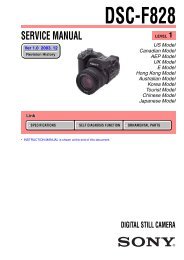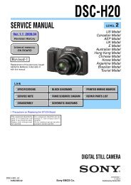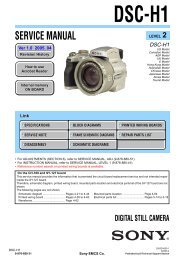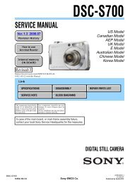
SERVICE MANUAL - SONYRUS
SERVICE MANUAL - SONYRUS
SERVICE MANUAL - SONYRUS

Create successful ePaper yourself
Turn your PDF publications into a flip-book with our unique Google optimized e-Paper software.
<strong>SERVICE</strong> <strong>MANUAL</strong><br />
Ver 1.2 2004.08<br />
Revision Revision History History<br />
How to use<br />
Acrobat Acrobat Reader Reader<br />
SPECIFICATIONS<br />
<strong>SERVICE</strong> NOTE<br />
DISASSEMBLY<br />
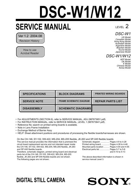
DSC-W1/W12<br />
BLOCK DIAGRAMS<br />
FRAME SCHEMATIC DIAGRAM<br />
SCHEMATIC DIAGRAMS<br />
LEVEL 2<br />
PRINTED WIRING BOARDS<br />
REPAIR PARTS LIST<br />
• For ADJUSTMENTS (SECTION 6), refer to <strong>SERVICE</strong> <strong>MANUAL</strong>, ADJ (987673651.pdf).<br />
• For INSTRUCTION <strong>MANUAL</strong>, refer to <strong>SERVICE</strong> <strong>MANUAL</strong>, LEVEL 1 (987673641.pdf).<br />
• Reference No. search on printed wiring boards is available.<br />
• Note in Lens Frame Installation<br />
• Exchange Method of Barrier Assy<br />
• HELP: Sheet attachment positions and procedures of processing the flexible boards/harnesses are shown.<br />
On the CH-146, SY-102, SW-422, MS-204, MS-205 flexible, JK-263 and SP-045 flexible boards<br />
This service manual procides the information that is premised the<br />
circuit board replacement service and not intended repair inside<br />
the CH-146, SY-102, SW-422, MS-204, MS-205 flexible, JK-263<br />
and SP-045 flexible boards.<br />
Therefore, schematic diagram, printed wiring board and electrical<br />
parts list of the CH-146, SY-102, SW-422, MS-204, MS-205<br />
flexible, JK-263 and SP-045 flexible boards are not shown.<br />
The following pages are not shown.<br />
DIGITAL STILL CAMERA<br />
DSC-W1<br />
US Model<br />
Canadian Model<br />
Hong Kong Model<br />
Australian Model<br />
Argentine Model<br />
Brazilian Model<br />
Tourist Model<br />
Japanese Model<br />
DSC-W1/W12<br />
AEP Model<br />
UK Model<br />
E Model<br />
Chinese Model<br />
Korea Model<br />
Schematic diagram ............... Pages 4-9 to 4-28<br />
Printed wiring board .............. Pages 4-39 to 4-48<br />
Mounted parts location.......... Pages 4-54 and 4-55<br />
Electrical parts list ................. Pages 5-7 to 5-8<br />
and 5-10 to 5-13<br />
The above-described information is shown in<br />
service manual Level 3.
DSC-W1/W12<br />
x Camera<br />
[System]<br />
Image device<br />
9.04 mm (1/1.8 type) color CCD<br />
Primary color filter<br />
Total pixels number of camera<br />
Approx. 5 255 000 pixels<br />
Effective pixels number of camera<br />
Approx. 5 090 000 pixels<br />
Lens Carl Zeiss Vario-Tessar<br />
3 zo om lens<br />
f = 7.9 – 23.7 mm (38 – 114 mm when<br />
converted to a 35 mm still camera)<br />
F2.8 – 5.2<br />
Exposure control<br />
Automatic exposure, Manual<br />
exposure, Twilight, Twilight portrait,<br />
Candle, Landscape, Beach, Soft snap<br />
White balance<br />
Automatic, Daylight, Cloudy,<br />
Fluorescent, Incandescent<br />
File format (DCF compliant)<br />
Still images: Exif Ver. 2.2 JPEG<br />
compliant, DPOF compatible<br />
Movies: MPEG1 compliant<br />
(Monaural)<br />
Recording media<br />
“Memory Stick”<br />
Flash Recommended distance (ISO set to<br />
Auto):<br />
0.2 m to 3.5 m (7 7/8 inches to 11 feet<br />
57/8 inches) (W)<br />
0.3 m to 2.5 m (11 7/8 inches to 8 feet<br />
21/2 inches) (T)<br />
[Input and Output connectors]<br />
A/V OUT (MONO) jack (Monaural)<br />
Minijack<br />
Video: 1 Vp-p, 75 Ω, unbalanced,<br />
sync negative<br />
Audio: 327 mV (at a 47 kΩ load)<br />
Output impedance 2.2 kΩ<br />
USB jack mini-B<br />
USB communication<br />
Hi-Speed USB (USB 2.0 compliant)<br />
[LCD screen]<br />
SPECIFICATIONS<br />
LCD panel<br />
6.2 cm (2.5 type) TFT drive<br />
Total number of dots<br />
123 200 (560×220) dots<br />
[Power, general]<br />
Power AA Nickel-Metal Hydride batteries (2)<br />
2.4 V<br />
AC-LS5 AC Adaptor<br />
(not supplied), 4.2 V<br />
Power consumption (during shooting with<br />
LCD screen on)<br />
1.4 W<br />
Operating temperature<br />
0°C to +40°C (+32°F to +104°F)<br />
Storage temperature<br />
–20°C to +60°C (–4°F to +140°F)<br />
Dimensions<br />
91 × 60 × 32.9 mm<br />
(3 5/8 × 2 3/8 × 1 5/16 inches)<br />
(W/H/D, excluding maximum<br />
protrusions)<br />
Mass Approx. 250 g (8.8 oz) (including two<br />
batteries, “Memory Stick” and wrist<br />
strap)<br />
Microphone<br />
Electret condenser microphone<br />
Speaker Dynamic speaker<br />
Exif Print Compatible<br />
PRINT Image Matching II<br />
Compatible<br />
PictBridge<br />
Compatible<br />
— 2 —<br />
x BC-CS2A/CS2B Ni-MH battery<br />
charger<br />
Power requirements<br />
AC 100 to 240V 50/60Hz<br />
3 W<br />
Output voltage<br />
AA : DC 1.4 V 400 mA × 2<br />
AAA : DC 1.4 V 160 mA × 2<br />
Operating temperature range<br />
0°C to +40°C (+32°F to +104°F)<br />
Storage temperature range<br />
–20°C to +60°C (–4°F to +140°F)<br />
Dimensions<br />
71 × 30 × 91 mm<br />
(2 7/8 × 1 3/16 × 3 5/8 inches) (W/H/D)<br />
Mass Approx. 90 g (3 oz)<br />
x AC-LS5 AC Adaptor (not supplied)<br />
Input rating<br />
100 V to 240 V AC, 50/60 Hz, 11 W,<br />
0.16 A to 0.09 A<br />
Output rating<br />
4.2 V DC, 1.5 A<br />
Operating temperature<br />
0°C to +40°C (+32°F to +104°F)<br />
Storage temperature<br />
–20°C to +60°C (–4°F to +140°F)<br />
Dimensions<br />
Approx. 48 × 29 × 81mm<br />
(1 15/16 × 1 3/16 × 3 1/4 inches)<br />
(W/H/D, excluding projecting parts)<br />
Mass Approx. 130 g (5 oz)<br />
x Accessories<br />
• HR6 (size AA) Ni-MH batteries (DSC-W1: 2,<br />
DSC-W12: 4)<br />
• Battery case (DSC-W1: 1, DSC-W12: 2)<br />
• BC-CS2A/CS2B Ni-MH Battery charger (1)<br />
• Power cord (mains lead) (1)<br />
• USB cable (1)<br />
• A/V connecting cable (1)<br />
• Wrist strap (1)<br />
• “Memory Stick” (32 MB) (1)<br />
• CD-ROM (USB driver SPVD-012) (1)<br />
• Operating instructions (1)<br />
• Soft carrying case (DSC-W12 only) (1)<br />
See page 5-15.<br />
Design and specifications are subject to change<br />
without notice.
SAFETY-RELATED COMPONENT WARNING!!<br />
COMPONENTS IDENTIFIED BY MARK 0 OR DOTTED LINE WITH<br />
MARK 0 ON THE SCHEMATIC DIAGRAMS AND IN THE PARTS<br />
LIST ARE CRITICAL TO SAFE OPERATION. REPLACE THESE<br />
COMPONENTS WITH SONY PARTS WHOSE PART NUMBERS<br />
APPEAR AS SHOWN IN THIS <strong>MANUAL</strong> OR IN SUPPLEMENTS<br />
PUBLISHED BY SONY.<br />
1. Check the area of your repair for unsoldered or poorly-soldered<br />
connections. Check the entire board surface for solder splashes<br />
and bridges.<br />
2. Check the interboard wiring to ensure that no wires are<br />
"pinched" or contact high-wattage resistors.<br />
3. Look for unauthorized replacement parts, particularly<br />
transistors, that were installed during a previous repair. Point<br />
them out to the customer and recommend their replacement.<br />
4. Look for parts which, through functioning, show obvious signs<br />
of deterioration. Point them out to the customer and<br />
recommend their replacement.<br />
5. Check the B+ voltage to see it is at the values specified.<br />
6. Flexible Circuit Board Repairing<br />
•Keep the temperature of the soldering iron around 270˚C<br />
during repairing.<br />
• Do not touch the soldering iron on the same conductor of the<br />
circuit board (within 3 times).<br />
• Be careful not to apply force on the conductor when soldering<br />
or unsoldering.<br />
SAFETY CHECK-OUT<br />
After correcting the original service problem, perform the following<br />
safety checks before releasing the set to the customer.<br />
— 3 —<br />
DSC-W1/W12<br />
ATTENTION AU COMPOSANT AYANT RAPPORT<br />
À LA SÉCURITÉ!<br />
LES COMPOSANTS IDENTIFÉS PAR UNE MARQUE 0 SUR LES<br />
DIAGRAMMES SCHÉMATIQUES ET LA LISTE DES PIÈCES SONT<br />
CRITIQUES POUR LA SÉCURITÉ DE FONCTIONNEMENT. NE<br />
REMPLACER CES COMPOSANTS QUE PAR DES PIÈSES SONY<br />
DONT LES NUMÉROS SONT DONNÉS DANS CE MANUEL OU<br />
DANS LES SUPPÉMENTS PUBLIÉS PAR SONY.<br />
Unleaded solder<br />
Boards requiring use of unleaded solder are printed with the leadfree<br />
mark (LF) indicating the solder contains no lead.<br />
(Caution: Some printed circuit boards may not come printed with<br />
the lead free mark due to their particular size.)<br />
: LEAD FREE MARK<br />
Unleaded solder has the following characteristics.<br />
• Unleaded solder melts at a temperature about 40°C higher than<br />
ordinary solder.<br />
Ordinary soldering irons can be used but the iron tip has to be<br />
applied to the solder joint for a slightly longer time.<br />
Soldering irons using a temperature regulator should be set to<br />
about 350°C.<br />
Caution: The printed pattern (copper foil) may peel away if the<br />
heated tip is applied for too long, so be careful!<br />
• Strong viscosity<br />
Unleaded solder is more viscous (sticky, less prone to flow) than<br />
ordinary solder so use caution not to let solder bridges occur such<br />
as on IC pins, etc.<br />
• Usable with ordinary solder<br />
It is best to use only unleaded solder but unleaded solder may<br />
also be added to ordinary solder.
DSC-W1/W12<br />
Section<br />
TABLE OF CONTENTS<br />
Title Page<br />
1. <strong>SERVICE</strong> NOTE<br />
1-1. Note for Repair ································································1-1<br />
1-2. Discharging of the ST-101 Flexible Board’s Charging<br />
Capacitors (C102 and C103) ···········································1-1<br />
1-3. Note in Lens Frame Installation ······································1-2<br />
1-4. Description on Self-diagnosis Display ····························1-2<br />
2. DISASSEMBLY<br />
2-1. Flow Chart ·······································································2-1<br />
2-2. SY-102 Board Service Position ·······································2-3<br />
2-3. Exchange Method of Barrier Assy ··································2-5<br />
2-3-1.Peel Off Old Ornamental Ring A ····································2-5<br />
2-3-2.Remove Old Barrier Assy ················································2-6<br />
2-3-3.Install New Barrier Assy ·················································2-6<br />
2-3-4.Adhere the Ornamental Ring A ·······································2-7<br />
2-4. Circuit Boards Location ··················································2-8<br />
3. BLOCK DIAGRAMS<br />
3-1. Overall Block Diagram (1/2) ···········································3-1<br />
3-2. Overall Block Diagram (2/2) ···········································3-3<br />
3-3. Power Block Diagram (1/2)·············································3-5<br />
3-4. Power Block Diagram (2/2)·············································3-7<br />
4. PRINTED WIRING BOARDS AND<br />
SCHEMATIC DIAGRAMS<br />
4-1. Frame Schematic Diagram ··············································4-1<br />
4-2. Schematic Diagrams ························································4-5<br />
CD-507 FLEXIBLE (CCD IMAGER) ····························4-7<br />
ST-100 (FLASH DRIVE) ··············································4-29<br />
ST-101 FLEXIBLE<br />
(CHARGING CAPACITOR, FLASH UNIT) ···············4-29<br />
US-011 FLEXIBLE (USB CONNECTOR) ··················4-31<br />
CONTROL SWITCH BLOCK ·····································4-32<br />
4-3. Printed Wiring Boards ···················································4-35<br />
CD-507 FLEXIBLE ······················································4-37<br />
ST-100 ···········································································4-49<br />
ST-101 FLEXIBLE ·······················································4-50<br />
US-011 FLEXIBLE ·······················································4-51<br />
4-4. Mounted Parts Location ················································4-53<br />
5. REPAIR PARTS LIST<br />
5-1. Exploded Views ·······························································5-2<br />
5-1-1.Cabinet Block Section ·····················································5-2<br />
5-1-2.Main Block Section ·························································5-3<br />
5-1-3.Lens Block Section ··························································5-4<br />
5-1-4.Side Frame Block Section ···············································5-5<br />
5-2. Electrical Parts List ·························································5-6<br />
— 4 —
1-1. NOTE FOR REPAIR<br />
Make sure that the flat cable and flexible board are not cracked of<br />
bent at the terminal.<br />
Do not insert the cable insufficiently nor crookedly.<br />
Cut and remove the part of gilt<br />
which comes off at the point.<br />
(Be careful or some<br />
pieces of gilt may be left inside)<br />
1-2. DISCHARGING OF THE ST-101<br />
FLEXIBLE BOARD’S CHARGING<br />
CAPACITORS (C102 AND C103)<br />
The charging capacitors (C102 and C103) of the ST-101 flexible<br />
board are charged up to the maximum 300 V potential.<br />
There is a danger of electric shock by this high voltage when the<br />
capacitor is handled by hand. The electric shock is caused by the<br />
charged voltage which is kept without discharging when the main<br />
power of the unit is simply turned off. Therefore, the remaining<br />
voltage must be discharged as described below.<br />
Preparing the Short Jig<br />
To preparing the short jig, a small clip is attached to each end of a<br />
resistor of 1 kΩ /1 W (1-215-869-11).<br />
Wrap insulating tape fully around the leads of the resistor to prevent<br />
electrical shock.<br />
1 kΩ/1 W<br />
Wrap insulating tape.<br />
SECTION 1<br />
<strong>SERVICE</strong> NOTE<br />
1-1<br />
When remove a connector, don’t pull at wire of connector.<br />
It is possible that a wire is snapped.<br />
DSC-W1/W12<br />
When installing a connector, don’t press down at wire of connector.<br />
It is possible that a wire is snapped.<br />
Discharging the Capacitor<br />
Short-circuit between the positive and the negative terminals of<br />
charged capacitor with the short jig about 10 seconds.<br />
ST-101<br />
Capacitor<br />
R:1 kΩ/1 W<br />
(Part code:<br />
1-215-869-11)<br />
ST kemikon sheet
DSC-W1/W12<br />
1-3. NOTE IN LENS FRAME INSTALLATION<br />
When tightening a screw, have both sides of the lens block assembly so as not for the load to depend.<br />
1-4. DESCRIPTION ON SELF-DIAGNOSIS DISPLAY<br />
Display Code Countermeasure<br />
C:32:ss Turn the power off and on again.<br />
C:13:ss<br />
Format the “Memory stick”.<br />
Insert a new “Memory Stick”.<br />
E:61:ss<br />
E:91:ss<br />
E:92:ss<br />
Lens block assembly<br />
Checking of lens drive circuit.<br />
Lens frame<br />
Self-diagnosis display<br />
• C: ss: ss<br />
You can reverse the camera<br />
malfunction yourself. (However,<br />
contact your Sony dealer or local<br />
authorized Sony service facility<br />
when you cannot recover from the<br />
camera malfunction.)<br />
• E: ss: ss<br />
Contact your Sony dealer or local<br />
authorized Sony service facility.<br />
1-2E<br />
Cause<br />
M1.4 × 4<br />
Trouble with hardware.<br />
Unformatted memory stick is inserted.<br />
Memory stick is broken.<br />
When failed in the focus and zoom<br />
initialization.<br />
Caution Display During Error<br />
SYSTEM ERROR<br />
FORMAT ERROR<br />
MEMORY STICK ERROR<br />
Checking of flash unit or replacement Abnormality when flash is being<br />
of flash unit. charged.<br />
—<br />
Insert batteries correctly. Batteries are not inserted correctly.<br />
Turn the power off and on again.<br />
Batteries were installed or removed when<br />
using the AC adaptor.
2-1. FLOW CHART<br />
The following flow chart shows the disassembly procedure.<br />
1 2<br />
3<br />
1 Ornamental ring (A)<br />
2 Tapping screw (M1.2) x2<br />
3 Barrier assy<br />
Note: When you exchange rings, be sure<br />
to follow the procedure carried on<br />
"2-3. Exchange Method of Barrier<br />
Assy" (2-5 page).<br />
1<br />
3<br />
SECTION 2<br />
DISASSEMBLY<br />
1 Lock ace screw (M1.7) x4<br />
2 Claw<br />
3 Rear cabinet<br />
4 Side cover<br />
5 Sheet (S)<br />
2<br />
4<br />
1<br />
HELP<br />
7<br />
6 Mic harness: CN102<br />
7 Lock ace screw (M1.7) x2<br />
8 Front cabinet<br />
8<br />
6<br />
5<br />
1<br />
2<br />
3<br />
2<br />
4<br />
6<br />
5<br />
9 qa<br />
8<br />
1 Claw x1 qs<br />
2 Claw x1<br />
3 Control SW block<br />
4 Control SW block flexible: CN702<br />
5 ST-101 flexible: CN601<br />
5<br />
4<br />
2-1 2-2<br />
0<br />
1<br />
1 BT terminal flexible: CN001<br />
2 Tapping screw (M1.7) x2<br />
3 SY-102<br />
4 MS-205 flexible: CN704<br />
5 Lock ace screw (M1.7) x2<br />
3<br />
7<br />
6<br />
0<br />
1<br />
0<br />
8<br />
9<br />
Note: High-voltage cautions<br />
Discharging the Capacitor<br />
Short-circuit between the two<br />
points with the short jig about 10<br />
seconds.<br />
ST-101<br />
9<br />
Capacitor<br />
R:1 kΩ/1 W<br />
(Part code:<br />
1-215-869-11)<br />
7<br />
6 Tapping screw (M1.7) x2<br />
7 Boss<br />
8 DC and A/V jack<br />
9 Claw x2<br />
0 MS-205<br />
ST kemikon sheet<br />
6 Claw x2<br />
7 Strobo block<br />
8 Tapping screw (M1.7) x1<br />
9 DC ground plate (B)<br />
0 Claw x2<br />
qa Claw x1<br />
qs Bottom cabinet<br />
8<br />
2<br />
4<br />
5<br />
1 3<br />
DSC-W1/W12<br />
HELP<br />
1 Open two connectors (CN201, 701)<br />
2 Claw x2<br />
3 Lens block<br />
4 CD-507: CN701<br />
5 Lens block flexible: CN201<br />
9<br />
6<br />
4<br />
1 Lock ace screw<br />
(M1.7) x2<br />
2 SW-422<br />
3 US-011 flexible: CN101<br />
4 Lock ace screw<br />
(M1.7) x1<br />
5 Claw x4<br />
1<br />
3<br />
0<br />
2<br />
2<br />
5<br />
5<br />
qa<br />
7<br />
6 US-011<br />
7 Claw x2<br />
8 Claw x2<br />
9 LCD block<br />
0 LCD flexible: CN801<br />
qa Back light<br />
flexible: CN802
DSC-W1/W12<br />
2-2. SY-102 BOARD <strong>SERVICE</strong> POSITION<br />
1<br />
3<br />
2<br />
2<br />
4<br />
4<br />
6<br />
5<br />
9<br />
8<br />
qa<br />
qs<br />
1<br />
3<br />
7<br />
0<br />
1<br />
7<br />
0<br />
8<br />
6<br />
5<br />
1<br />
2<br />
3<br />
8<br />
2<br />
1 3<br />
4<br />
5<br />
9<br />
6<br />
4<br />
5<br />
4<br />
1<br />
1<br />
0<br />
6<br />
3<br />
0<br />
2<br />
8<br />
5<br />
5<br />
qa<br />
2<br />
9<br />
9<br />
7<br />
7<br />
MS-205 flexible board<br />
LCD block<br />
US-011 flexible board<br />
2-3 2-4<br />
AC power<br />
adaptor<br />
AC IN<br />
SW-422 board<br />
Color monitor<br />
SY-102 board<br />
Control switch block<br />
Stroboscope block<br />
Lens block
2-3. EXCHANGE METHOD OF BARRIER ASSY<br />
Service parts<br />
Part Number Part Name Quantity<br />
1 3-091-427-01 Ring (A), Ornamental 1<br />
2 X-3954-476-1 Barrier Assy 1<br />
3 3-086-156-31 Tapping screw (P2) 2<br />
Tools used<br />
Torque driver<br />
Soldering iron<br />
Weight about 60g<br />
Adhesive (Super X) (Note)<br />
Note: Use adhesive (Super X) or an equivalent article.<br />
Don’t use what becomes white after drying like a quick-drying glue.<br />
2-3-1. PEEL OFF OLD ORNAMENTAL RING A<br />
2-5<br />
DSC-W1/W12<br />
The Ornamental Ring A has adhered to the Barrier Assy strongly and accordingly, use a soldering iron to weaken the adhesive force.<br />
Heat four circled portions with the soldering iron.<br />
Heating temperature is about 300ºC.<br />
Beware of a burn since the entire Ornamental Ring becomes hot.<br />
* As the adhesive force of Ornamental Ring A is considerably large, the forced peeling will damage the group-1 frame.<br />
Insert the tip of tweezers, etc. into a notch of the group-1 frame and prize the ring.<br />
* Take extreme care so as not to damage the coated surface of the group-1 frame.<br />
In case of difficult peeling, heat the ring again with the soldering iron.<br />
If this re-heating failed, it may be advisable that the ring be peeled while heating the portions 1 → 2 → 3 → 4 in the under figure one<br />
by one sequentially.<br />
* Discard the removed Ornamental Ring A.<br />
Tip<br />
2<br />
4<br />
1<br />
3<br />
1<br />
2<br />
3
DSC-W1/W12<br />
2-3-2. REMOVE OLD BARRIER ASSY<br />
1 Remove two screws.<br />
* Discard the removed screws.<br />
2 Remove the Barrier Assy.<br />
* Discard the removed Barrier Assy.<br />
* After removing the Barrier Assy, if the “G1 Dust-Proof Ring” was removed, it must be returned to the home position.<br />
In returning the ring, adjust the location of a projection to the lens direction.<br />
This is an important part to prevent the dust and light from coming in.<br />
* After removing the Barrier Assy, take extreme care not to drop dust or foreign substances in the lens barrel.<br />
2-3-3. INSTALL NEW BARRIER ASSY<br />
1 Install new Barrier Assy by paying attention to the projection of the Barrier Assy in relation to the position shown in the under figure.<br />
2 Tighten two screws.<br />
* Tightening torque = 0.5 kgf<br />
1<br />
1<br />
1<br />
Projection<br />
2-6<br />
2<br />
2<br />
2
2-3-4. ADHERE THE ORNAMENTAL RING A<br />
Apply an adhesive to four recesses on the top surface of the Barrier Assy.<br />
* Do not apply too much adhesive. (Make quantity of adhesives into the quantity in which a groove hides.)<br />
2-7<br />
DSC-W1/W12<br />
Meeting a “notch” of the Ornamental Ring A with a “projection” of the group-1 frame, push the Ornamental Ring A into the group-1 frame.<br />
* The projection of the spring for preventing static electricity must be tilted.<br />
Put the 60g weight on the Ornamental Ring A so that the Ornamental Ring A does not float up until the adhesive hardens.<br />
Note: Be careful not to give a shock.<br />
* After the weight was put, no gap must be present in full circumference between Ornamental Ring A and group-1 frame.<br />
A gap, if present, causes the crackle sound NG.<br />
* The weight must push in the Ornamental Ring A only.<br />
If the weight is put on the mold part of the Barrier Assy, the Ornamental Ring A will float up.<br />
Notch<br />
Adhesive<br />
Projection<br />
Adhesive<br />
Completion after 30 minutes.<br />
Adhesive<br />
Adhesive<br />
Do not put the weight on a black mold part.<br />
Not gap in full circumference.
DSC-W1/W12<br />
2-4. CIRCUIT BOARDS LOCATION<br />
SY-102<br />
(including CH-146)<br />
CH-146<br />
(included in SY-102)<br />
US-011 flexible<br />
CD-507 flexible<br />
2-8E<br />
SW-422<br />
MS-204<br />
ST-100<br />
ST-101 flexible<br />
MS-205 flexible<br />
JK-263<br />
SP-045 flexible<br />
Board Name Function<br />
CD-507 flexible CCD IMAGER<br />
CH-146 CCD SIGNAL PROCESS<br />
(included in SY-102)<br />
JK-263 JACK<br />
MS-204 LCD DRIVE, MS CONNECTOR<br />
MS-205 flexible CONNECTOR<br />
SP-045 flexible SPEAKER<br />
ST-100 FLASH DRIVE<br />
ST-101 flexible CHARGING CAPACITOR, FLASH UNIT<br />
SY-102 CAMERA MODULE, CAMERA DSP, LENS DRIVE,<br />
(Including CH-146) SH DSP, FRONT CONTROL, DC/DC CONVERTER<br />
SW-422 AUDIO, CONTROL SWITCH<br />
US-011 flexible USB CONNECTOR
Mic harness<br />
US-011 flexible board<br />
HELP<br />
Sheet attachment positions and procedures of processing the flexible boards/harnesses are shown.<br />
Sheet (S)<br />
Front side<br />
DSC-W1/W12<br />
HELP
Link<br />
OVERALL BLOCK DIAGRAM (1/2)<br />
3. BLOCK DIAGRAMS<br />
POWER BLOCK DIAGRAM (1/2)<br />
OVERALL BLOCK DIAGRAM (2/2) POWER BLOCK DIAGRAM (2/2)<br />
DSC-W1/W12
SECTION 3<br />
BLOCK DIAGRAMS<br />
3-1. OVERALL BLOCK DIAGRAM (1/2)<br />
FLASH<br />
UNIT<br />
SHUTTER<br />
MOTOR<br />
M<br />
05<br />
LENS<br />
ZOOM<br />
FG<br />
LENS BLOCK<br />
ZOOM<br />
MOTOR<br />
M<br />
ZOOM<br />
SENSOR<br />
FOCUS<br />
SENSOR<br />
FOCUS<br />
MOTOR<br />
M<br />
LENS TEMP<br />
SENSOR<br />
IRIS<br />
(METER)<br />
ST-101 FLEXIBLE BOARD<br />
XE_H<br />
TRIG 300V<br />
XE_L<br />
C102, 103<br />
CHARGING<br />
CAPACITOR<br />
+ +<br />
IRIS<br />
MOTOR<br />
M<br />
ST-100 BOARD<br />
CL001,<br />
003 – 007,<br />
042<br />
CL022<br />
CL021, 043<br />
Q003<br />
D005<br />
2<br />
IC001<br />
CD-507 FLEXIBLE BOARD (1/2)<br />
2<br />
FLASH<br />
CONTROL<br />
IC101<br />
CCD<br />
IMAGER<br />
T001<br />
5 4<br />
4<br />
1<br />
3<br />
17<br />
19<br />
23<br />
25<br />
24<br />
30<br />
31<br />
4<br />
8<br />
ı<br />
10<br />
12<br />
ı<br />
15<br />
1<br />
3<br />
5<br />
6<br />
11<br />
7<br />
26<br />
27<br />
Q103<br />
XSTB FULL<br />
STB ON<br />
Q102<br />
BUFFER<br />
F MOTOR A, A, B, B<br />
Z DC MOTOR ±<br />
IRIS M±, S±<br />
SHUTTER ±<br />
F PI SENS OUT<br />
Z PI SENS OUT<br />
Z BOX1 PI SENS OUT,<br />
Z BOX2 PI SENS OUT<br />
Q001, 002<br />
TRANS<br />
DRIVE<br />
Q105<br />
LENS TEMP<br />
16<br />
4<br />
10<br />
7<br />
9<br />
6<br />
34<br />
30 ı<br />
28<br />
26 ı<br />
23<br />
24 ı<br />
27<br />
17 ı<br />
20<br />
5 ı<br />
8<br />
1 ı<br />
4<br />
29<br />
21<br />
31<br />
SY-102 BOARD (1/2)<br />
CN701<br />
(1/2)<br />
CN201<br />
FOCUS A, A, B, B<br />
ZOOM DC ±<br />
IRIS M±, S±<br />
SHUTTER±<br />
86<br />
133<br />
33<br />
42<br />
51<br />
A6<br />
B5<br />
A4<br />
B4<br />
C1<br />
D2<br />
G5<br />
H6<br />
G4<br />
H4<br />
E7<br />
D7<br />
Q602, 603<br />
FOCUS<br />
MOTOR<br />
DRIVER<br />
ZOOM<br />
MOTOR<br />
DRIVER<br />
IRIS<br />
MOTOR<br />
DRIVER<br />
B1<br />
G3<br />
H2<br />
G2<br />
G1<br />
SHUTTER F8<br />
MOTOR F7<br />
DRIVER H8<br />
ST UNREG<br />
3. BLOCK DIAGRAMS<br />
( ) : Number in parenthesis ( ) indicates the division number of schematic diagram where the component is located.<br />
RG, H1B, H2B<br />
H1A, H2A<br />
V2, V4, V5A, V5B,<br />
V6, V7A, V7B, V8<br />
V1A, V1B,<br />
V3A, V3B<br />
VHOLD<br />
VST<br />
VSUB<br />
VSUB CONT<br />
CL025 – 030,<br />
044, 045<br />
CL039<br />
CL038<br />
CL041<br />
19<br />
36<br />
35<br />
33<br />
32<br />
27<br />
31<br />
21<br />
20<br />
12<br />
15<br />
12 ı<br />
17<br />
3<br />
4<br />
1<br />
Q701<br />
CN601<br />
ST UNREG<br />
STB FULL<br />
STB ON<br />
CCD OUT<br />
POWER SAVE<br />
Q105<br />
Q205<br />
6<br />
37<br />
5<br />
2<br />
4<br />
1<br />
3<br />
9<br />
12<br />
ı<br />
18<br />
7<br />
8<br />
10<br />
11<br />
20<br />
19<br />
21<br />
36<br />
CH-146 BOARD<br />
37<br />
48<br />
113 109<br />
112 115<br />
125 119<br />
118 121<br />
10<br />
13<br />
17<br />
20<br />
7<br />
11<br />
19<br />
135<br />
134 136 2 4<br />
6 9 12 15<br />
18 21 24<br />
27 30 32<br />
49 105<br />
66 101 120<br />
99<br />
IC101<br />
CCD SIGNAL<br />
PROCESSOR,<br />
TIMING<br />
GENERATOR<br />
Q604<br />
132<br />
124<br />
3 123<br />
126–129<br />
84<br />
22 ı<br />
35<br />
45<br />
46<br />
48<br />
40 ı<br />
42<br />
47<br />
CP101<br />
CAMERA<br />
MODULE<br />
(1/6)<br />
IC201<br />
STRB CHRG<br />
XSTRB FULL<br />
XFE CS, XTG CS<br />
TG CLK<br />
X301<br />
54MHz<br />
LENS DRIVE<br />
(3/6)<br />
B7<br />
B8<br />
C7<br />
C8<br />
B3<br />
A2<br />
38<br />
39<br />
XSTRB PWR SAVE XSTRB PWR SAVE<br />
CAM F<br />
1<br />
HR EN2,<br />
HR DIR2A,<br />
HR DIR2B<br />
HR EN0,<br />
HR DIR0A<br />
XZM DC BR<br />
IRIS M IN<br />
IRIS M EN<br />
IRIS S IN<br />
IRIS S EN<br />
XFC RST SENS<br />
XZM RST SENS1<br />
CA HD<br />
CAM F<br />
MCKTG<br />
IC304<br />
MSHUT DIR<br />
MSHUT EN<br />
MSHUT REF<br />
ZM DC FG A, B<br />
CA AD00 – CA AD13<br />
CAM SO, XCAM SCK, XCAM RST<br />
CLOCK<br />
GENERATOR<br />
(2/6)<br />
27MHz<br />
5<br />
VER EXT CLK<br />
CAM SO, XCAM SCK, XCAM RST<br />
Y11 AB11 Y10<br />
AA11 AB10 Y9<br />
AB9 AA10 AA9<br />
Y8 AB8 AA8<br />
AB7 AA7<br />
Y7<br />
AB6<br />
AC8<br />
AC22<br />
N3<br />
K3<br />
M4<br />
K4<br />
J3<br />
T4<br />
U2<br />
T3<br />
T2<br />
U3<br />
AA19<br />
F4<br />
F3<br />
G4 J2 Y4<br />
G3 H4 W4<br />
STRB ON<br />
AB20<br />
IC301<br />
CAMERA DSP,<br />
SDRAM<br />
(KWF BOARD)<br />
(2/6)<br />
F1<br />
D1<br />
E1<br />
C6<br />
D7<br />
G1<br />
AC12<br />
AC15<br />
P4<br />
D8<br />
AA12<br />
J23<br />
J22<br />
U20 V21 V23 U22<br />
V20 V22 W20 Y20<br />
W22 Y23 W21 Y22<br />
Y21 AA22 AA21 AB22<br />
J21 L22 L20 L23 K21<br />
L21 M21 M23 M20 M22<br />
N21 N22 N20 P20 P21<br />
P23 R21 P22 T21 R23<br />
R20 R22 T20 T23 U21<br />
P1<br />
CAM SO, XCAM SCK, XCAM RST<br />
A : VIDEO SIGNAL<br />
A : AUDIO SIGNAL<br />
A : VIDEO/AUDIO SIGNAL<br />
PANEL R<br />
PANEL G<br />
PANEL B<br />
HDO<br />
PANEL V<br />
SYS SI, SYS SO, XSYS SCK<br />
XSYS RST<br />
SYS V<br />
XSYS RST<br />
XPANEL TG CS<br />
BL LEV<br />
MC XCS IC 301REG<br />
MC XCS IC 301SDRAM<br />
MC D0 – D15<br />
MC A1 – A25<br />
MC CKIO<br />
CN704 CN001<br />
(1/3) (1/3)<br />
13 13<br />
11 11<br />
9 9<br />
CL819<br />
CL820<br />
CL821<br />
CL804,<br />
BL H<br />
BL L<br />
807, 808<br />
14 14<br />
CL801–803<br />
27 27<br />
VIDEO AMP ON<br />
XPANEL TG CS<br />
SYS SI, SYS SO, XSYS SCK<br />
CAM F<br />
XFE CS<br />
XTG CS<br />
LENS TEMP<br />
D21<br />
AD16<br />
A11<br />
B11<br />
C11<br />
D14<br />
K2<br />
AA8<br />
VER EXT CLK<br />
A6<br />
XZM DC BR<br />
AA19<br />
MSHUT REF<br />
G2<br />
XSTRB PWR SAVE<br />
AB11<br />
STRB CHRG<br />
AD19<br />
XSTRB FULL<br />
AC15<br />
3-1 3-2<br />
19 19<br />
17 17<br />
21 21<br />
2<br />
8<br />
6<br />
4<br />
10<br />
2<br />
8<br />
6<br />
4<br />
10<br />
MS-205 FLEXIBLE BOARD (1/3)<br />
CL816<br />
CL815<br />
CL817<br />
CL811,<br />
813, 814<br />
CL812<br />
CL810<br />
4<br />
1<br />
IC302<br />
VIDEO AMP<br />
(2/6)<br />
IC501<br />
MC CAM,<br />
SH DSP,<br />
FLASH<br />
(4/6)<br />
A17<br />
C18<br />
L21 L23 M24 K23<br />
H22 J21 J22 F24<br />
K21 H21 M23 K22<br />
G21 L24 F23 E23<br />
V22 V21 V23 R22 W22<br />
U22 W21 T22 R23 N21<br />
P22 P21 P23 R21 M22<br />
T21 P24 U21 U23 N22<br />
U24 N23 T24 M21 T23<br />
A7<br />
H1<br />
AC12<br />
AA9<br />
AC16<br />
A2<br />
A12<br />
B12<br />
C23<br />
MS-204 BOARD (1/3)<br />
D11<br />
E11<br />
F11<br />
A2<br />
B1<br />
C1<br />
A5<br />
B4<br />
A4<br />
B5<br />
G10<br />
2<br />
AA18<br />
D22<br />
AB7<br />
AD14<br />
J1<br />
K1<br />
L1<br />
M1<br />
L22<br />
AD20<br />
B16<br />
B15<br />
D16<br />
C22<br />
AB5<br />
AB13<br />
B13<br />
D13<br />
C13<br />
IC801<br />
LCD DRIVE<br />
L6<br />
L7<br />
L8<br />
J11<br />
V OUT<br />
AU AIN<br />
AU AOUT<br />
USBPHY D±<br />
MC MSDIO,<br />
MC MSBS,<br />
MC MSCLK<br />
FR SI, FR SO, XFR SCK<br />
XSYS RST<br />
SYS V<br />
CN801<br />
VR<br />
VG<br />
VB<br />
COM<br />
RGT, HCK1, HCK2,<br />
HST, PCG, XSTBY,<br />
E1 F1 G2<br />
DWN, EN, VST,<br />
H2 H1 J2<br />
VCK, REF, VP<br />
J1 K1 K3<br />
L3 H11<br />
K11 L10<br />
XAU LINE MUTE<br />
AU SEN<br />
MELODY ENV<br />
MELODY<br />
TALLY LED<br />
XAE LOCK LED ON<br />
XACCESS LED<br />
PRELAMP AF CONT<br />
F1<br />
SELF TIMER LED<br />
H23<br />
AD11<br />
D11<br />
LED K<br />
LED A<br />
BL LEV<br />
SYS SO, XSYS SCK<br />
XAE LOCK ON<br />
XSHTR ON<br />
FR INT<br />
XCS MC<br />
Q702<br />
LED<br />
DRIVE<br />
CN802<br />
BL H<br />
3<br />
BL L<br />
1<br />
3<br />
1<br />
CN701<br />
(2/2)<br />
2<br />
4<br />
5<br />
3<br />
23<br />
24<br />
2<br />
6 ı<br />
8<br />
11 ı<br />
14<br />
19 ı<br />
22<br />
DSC-W1/W12<br />
OVERALL (2/2)<br />
(PAGE 3-4)<br />
OVERALL (2/2)<br />
(PAGE 3-3)<br />
39<br />
OVERALL (2/2)<br />
(PAGE 3-3)<br />
PANEL UNIT<br />
LCD901<br />
COLOR<br />
LCD<br />
MONITOR<br />
D901<br />
BACKLIGHT<br />
CD-507 FLEXIBLE<br />
BOARD (2/2)<br />
XLED<br />
D101<br />
SELF TIMER/<br />
AF ILLUMINATOR
DSC-W1/W12<br />
SY-102 BOARD (2/2)<br />
MODE<br />
DIAL<br />
OVERALL (1/2)<br />
(PAGE 3-2)<br />
CONTROL SWITCH BLOCK<br />
D002<br />
SELF TIMER/<br />
RECORDING<br />
D003<br />
(AE/AF LOCK)<br />
D004<br />
(FLASH CHARGE)<br />
D001<br />
(POWER)<br />
S201 – 208<br />
FUNCTION<br />
KEY<br />
SW-422 BOARD (2/2)<br />
05<br />
1<br />
XTALLY LED<br />
XAE LOCK LED<br />
XCHARGE LED<br />
S001<br />
(SHUTTER)<br />
CN101<br />
(3/3)<br />
S002<br />
POWER<br />
1<br />
2<br />
USBPHY D± USBPHY D±<br />
MELODY<br />
TALLY LED<br />
XAE LOCK LED ON<br />
CN702<br />
9<br />
8<br />
6<br />
XCHARGE/XSTRB LED<br />
XPWR ON<br />
USB JACK IN<br />
CN101<br />
(1/3)<br />
SW-422 BOARD<br />
(1/2)<br />
AU AIN<br />
AU AOUT<br />
26<br />
18<br />
AU AIN<br />
AU OUT<br />
19<br />
10<br />
H6<br />
H7<br />
A7<br />
SYS SO, XSYS SCK<br />
15<br />
22<br />
7<br />
15<br />
SYS SO, XSYS SCK<br />
H2<br />
H3<br />
IC151<br />
AUDIO AMP<br />
XAU LINE MUTE<br />
AU SEN<br />
23<br />
21<br />
XAU LINE MUTE<br />
16<br />
AU SEN<br />
14<br />
G4<br />
H4<br />
A2<br />
A4<br />
MELODY ENV<br />
Q502<br />
MODULATOR<br />
20<br />
BEEP<br />
12<br />
C1<br />
F1<br />
10<br />
11<br />
3<br />
2<br />
4<br />
1<br />
XSHTR ON<br />
XAE LOCK ON<br />
US-011 FLEXIBLE BOARD (1/2)<br />
XCHARGE/XSTRB LED<br />
MODE DIAL0, 1 MODE DIAL0, 1<br />
XPWR LED<br />
Q501<br />
LED<br />
DRIVE<br />
Q503<br />
LED<br />
DRIVE<br />
US-011 FLEXIBLE BOARD (2/2)<br />
KEY AD0, 1 9<br />
CN703<br />
(3/3)<br />
KEY AD0, 1<br />
S001 S002<br />
(ZOOM)<br />
10<br />
T<br />
W<br />
KEY AD2<br />
OVERALL (1/2)<br />
(PAGE 3-2)<br />
CN001<br />
VCC<br />
2<br />
2<br />
3<br />
1<br />
(USB)<br />
FR INT<br />
XCS MC<br />
XSYS RST<br />
SYS V<br />
XAE LOCK ON<br />
XSHTR ON<br />
USB JACK IN<br />
FR SI, FR SO, XFR SCK<br />
Q402<br />
XPWR ON<br />
XPOWER LED ON<br />
X401<br />
32.768kHz<br />
PLL<br />
LOOP<br />
FILTER<br />
KEY AD0, 1<br />
KEY AD2<br />
C8<br />
D1<br />
D2<br />
E1<br />
D9<br />
E2<br />
B3<br />
B9<br />
B1<br />
J8<br />
J9<br />
B8 J5<br />
J4<br />
B2<br />
J2<br />
J3<br />
3. BLOCK DIAGRAMS<br />
3-2. OVERALL BLOCK DIAGRAM (2/2) ( ) : Number in parenthesis ( ) indicates the division number of schematic diagram where the component is located.<br />
BT001<br />
LITHIUM<br />
BATTERY<br />
2<br />
33<br />
CN703<br />
(1/3)<br />
5<br />
7<br />
3<br />
D±<br />
J6<br />
H6<br />
G6<br />
CN102<br />
MIC IN<br />
2<br />
CN101<br />
(2/3)<br />
23<br />
24<br />
IC401<br />
21<br />
FRONT<br />
CONTROLLER<br />
(5/6)<br />
A3<br />
B6<br />
A7<br />
D7<br />
C1<br />
D3<br />
H1<br />
E8<br />
H2<br />
A9<br />
MIC901<br />
SP±<br />
AU AOUT<br />
AV JACK IN<br />
Q401<br />
30<br />
31<br />
28<br />
CN703<br />
(2/3)<br />
DDCON SO, DDCON SCK<br />
XCS DDCON<br />
SYS DD ON<br />
FAST CHARGE<br />
XMS IN<br />
V OUT<br />
41 41<br />
V OUT CL919 CL924 CL112 V OUT<br />
AU OUT<br />
34 34<br />
AU OUT CL920 CL925 CL113 AU OUT<br />
L8<br />
K8<br />
K7<br />
C7<br />
D7<br />
E3<br />
E4<br />
ACV UNREG<br />
ST UNREG<br />
BATT/XEXT<br />
PANEL 8.5V<br />
EVER 3.0V<br />
IC001<br />
A 3.1V<br />
DC/DC<br />
D 1.2V<br />
D 2.8V<br />
A 2.8V<br />
CAM 15.5V<br />
CAM –7.5V/–8.0V<br />
CAM 3.3V<br />
M 5V<br />
ST 5V<br />
CONTROL,<br />
RESET<br />
(6/6)<br />
G1<br />
G2<br />
B1<br />
ACV UNREG<br />
LED A<br />
3<br />
LED K<br />
BL LEV OVERALL (1/2)<br />
(PAGE 3-2)<br />
BATT IN<br />
VL 3V VL 3V<br />
SP±<br />
XACCESS LED<br />
CN704 (2/3)<br />
MS-205 FLEXIBLE BOARD (2/3)<br />
CN001 (2/3)<br />
JK-263 BOARD<br />
(1/2)<br />
SP-045 FLEXIBLE<br />
BOARD<br />
30 30<br />
28 28<br />
SP± CL144, 145 SP±<br />
LND006, 007 LND008, 009<br />
AV JACK IN CL918<br />
XRSTX CL901 XRSTX<br />
29 29<br />
CHG SW<br />
CL916<br />
BATT UNREG<br />
XRSTX<br />
BACK UP VCC<br />
Q010<br />
CL923 CL111<br />
MS-204 BOARD<br />
V OUT<br />
16 16<br />
CL905,<br />
909, 911<br />
(2/3) CN901<br />
4<br />
MC MSDIO, MC MSBS, MC MSCLK<br />
XACCESS LED<br />
MC MSDIO, MC MSBS, MC MSCLK 33 33<br />
37 37<br />
35 35<br />
XMS IN<br />
MC MSDIO, MC MSBS, MC MSSCLK<br />
CL907 XMS IN<br />
2<br />
8<br />
6<br />
MEMORY<br />
STICK<br />
4 5<br />
IC002<br />
INITIAL<br />
RESET,<br />
BACK UP VCC<br />
(6/6)<br />
3-3 3-4<br />
3<br />
2<br />
38 38<br />
40 40<br />
Q902<br />
LED<br />
DRIVE<br />
CL917<br />
Q001<br />
CL118<br />
AV JACK IN<br />
42 42<br />
CN001<br />
6<br />
ı<br />
10<br />
D105<br />
(MS ACCESS)<br />
1 ı<br />
5<br />
ACV UNREG1<br />
+<br />
−<br />
J101<br />
AV OUT<br />
(MONO)<br />
MS-205 FLEXIBLE BOARD<br />
CN704 (3/3) CN001 (3/3)<br />
(3/3)<br />
44 44<br />
46 46<br />
48 48<br />
50 50<br />
43 43<br />
45 45<br />
47 47<br />
49 49<br />
CL922<br />
BATT UNREG<br />
BATT GND<br />
GND<br />
BATT/XEXT<br />
CL927<br />
BT901<br />
BATTERY<br />
TERMINAL<br />
MS-204 BOARD<br />
(3/3)<br />
A : VIDEO SIGNAL<br />
A : AUDIO SIGNAL<br />
A : VIDEO/AUDIO SIGNAL<br />
JK-263 BOARD<br />
(2/2)<br />
CL101–104<br />
CL105–108<br />
CL109<br />
S901<br />
RESET<br />
SP901<br />
SPEAKER<br />
J102<br />
DC IN
05<br />
SY-102 BOARD (1/2)<br />
D001, 002<br />
D012<br />
D 1.2V<br />
BATT UNREG<br />
ACV UNREG<br />
D008<br />
IC401<br />
FRONT CONTROLLER<br />
(5/6)<br />
G8 ACV SENS<br />
H8 BATT SENS<br />
F8 DD CON SENS<br />
A7 BATT/XEXT<br />
3. BLOCK DIAGRAMS<br />
3-3. POWER BLOCK DIAGRAM (1/2) ( ) : Number in parenthesis ( ) indicates the division number of schematic diagram where the component is located.<br />
J102<br />
DC IN<br />
JK-263 BOARD<br />
CL101–104<br />
CL105–108<br />
CL109<br />
BT901<br />
BATTERY<br />
TERMINAL<br />
+<br />
−<br />
BATT UNREG<br />
BATT GND<br />
MS-205 FLEXIBLE BOARD<br />
(1/3)<br />
CN001<br />
(1/3)<br />
ACV UNREG1<br />
GND<br />
CL927 BATT/XEXT CL922<br />
MS-204 BOARD<br />
(1/3)<br />
6 ı<br />
10<br />
1 ı<br />
5<br />
44 44<br />
46 46<br />
48 48<br />
50 50<br />
42 42<br />
43 43<br />
45 45<br />
47 47<br />
49 49<br />
CN001<br />
CN704<br />
(1/3)<br />
Q001<br />
Q010<br />
US-011 FLEXIBLE<br />
BOARD (1/2)<br />
CN703<br />
(1/2)<br />
BT001<br />
LITHIUM<br />
BATTERY<br />
VL 3V<br />
33<br />
VL 3V<br />
Q002<br />
F003<br />
F001<br />
F002<br />
Q003, 011<br />
DC CONTROL<br />
IC002<br />
INITIAL RESET,<br />
BACK UP VCC<br />
(6/6)<br />
D005<br />
A9<br />
C1<br />
D3<br />
H1<br />
H2<br />
E8<br />
F005<br />
2 VCH<br />
BATT IN<br />
VIN 7<br />
3 VBAT VOUT 6<br />
4 CS<br />
BACK UP VCC<br />
L001, 002<br />
L015<br />
L014<br />
L006<br />
DDCON SO,<br />
DDCON SCK<br />
XCS DDCON<br />
FAST CHARGE<br />
SYS DD ON<br />
D9 OUT8A<br />
E9 OUT8B<br />
B11 VCC8<br />
C10 VCH8A<br />
C11 VCH8B<br />
E8 CPSW<br />
C9 ODP SW<br />
E4 CHG SW<br />
D1 VDCIN<br />
H6 TLD<br />
G11 VCC1A<br />
G10 VCC1B<br />
G9 VCC1C<br />
F9 VCC2<br />
J3 OUT3A<br />
K1 OUT3B<br />
J2 OUT3C<br />
K5 VCC5<br />
L8 DIN<br />
K8 CLK<br />
K7<br />
E3<br />
LD<br />
FCHG<br />
IC001<br />
DC/DC CONTROL<br />
(6/6)<br />
C7 SYSDDON<br />
D7 USB PWR ON<br />
MARK E5<br />
BATT D4<br />
VCH1A L10<br />
VCH1B K9<br />
VCH1C (FB4) L9<br />
VLDO1 A11<br />
VCH2 E11<br />
OUT2 F10<br />
VCH3A (FB3) J1<br />
VCH3B H4<br />
VCH3C (FB6) H3<br />
VCH3S H2<br />
VCC GD H1<br />
VOS72 K4<br />
VOS73 L3<br />
VCH7 K3<br />
D 1.2V<br />
ACV UNREG<br />
L003<br />
VCH4 J6<br />
D010<br />
OUT4 K6<br />
VLDO4 C8<br />
VCH5 J5<br />
D009<br />
OUT5 L5<br />
VLDO5 B8<br />
VCH6 G1<br />
D006<br />
OUT6 F1<br />
ICH6 G2<br />
REF6 B1<br />
VCC7 J4<br />
L007<br />
L011<br />
L004 F004<br />
Q007, 008<br />
SWITCHING<br />
Q009<br />
DC CONTROL<br />
3-5 3-6<br />
L013<br />
L012<br />
CN702<br />
EVER 3.0V<br />
14<br />
ST UNREG<br />
A 2.8V<br />
D 2.8V<br />
D 1.2V<br />
M 5V<br />
ST 5V<br />
CAM 15.5V<br />
A 3.1V<br />
CAM –7.5V/–8.0V<br />
D004<br />
D 2.8V<br />
D 2.8V<br />
PANEL 8.5V<br />
LED A<br />
LED K<br />
BL THH<br />
BL LEV<br />
CAM 3.3V<br />
13<br />
12<br />
CONTROL SWITCH BLOCK<br />
A<br />
D 2.8V<br />
POWER 2<br />
(PAGE 3-7)<br />
D001<br />
(POWER)<br />
D004<br />
(FLASH CHARGE)<br />
D002<br />
SELF TIMER/<br />
RECORDING<br />
D003<br />
(AE/AF LOCK)<br />
DSC-W1/W12
DSC-W1/W12<br />
3-4. POWER BLOCK DIAGRAM (2/2)<br />
05<br />
SY-102 BOARD (2/2)<br />
POWER 1<br />
(PAGE 3-6)<br />
A<br />
ST UNREG<br />
ST 5V<br />
PANEL 8.5V<br />
BL LEV BL LEV<br />
CL810<br />
BL LEV<br />
10 10<br />
BL THH<br />
LED A<br />
LED K<br />
CAM 3.3V<br />
CAM 15.5V<br />
CAM –7.5V/–8.0V<br />
M 5V<br />
A 2.8V<br />
D 2.8V<br />
A 3.1V<br />
D 1.2V<br />
US-011 FLEXIBLE BOARD (2/2)<br />
SW-422 BOARD<br />
IC151<br />
AUDIO AMP<br />
L152<br />
CN101<br />
5<br />
6<br />
8<br />
17<br />
L601<br />
AU 5V<br />
A 2.8V<br />
AU 2.8V<br />
Q602, 603<br />
13<br />
14<br />
16<br />
24<br />
CN703<br />
(2/2)<br />
AU 5V<br />
A 2.8V<br />
AU 2.8V<br />
M 5V (PANEL 5V)<br />
A 2.8V (PANEL 2.8V)<br />
M 5V (AU_5V)<br />
A 2.8V<br />
CN601<br />
BL THH<br />
BL H<br />
BL L<br />
IC001<br />
CN704 CN001<br />
(2/3) (2/3) MS-204 BOARD (2/3)<br />
L803<br />
PANEL 8.5V CL826–828 PANEL 8.5V<br />
3 3<br />
PANEL 4.9V<br />
PANEL 2.8V<br />
1<br />
1<br />
12 12<br />
14 14<br />
27 27<br />
CL040<br />
MS-205 FLEXIBLE BOARD (2/3)<br />
PANEL 4.9V<br />
5 2.8V 4<br />
PANEL 2.8V REG<br />
D 2.8V<br />
D 1.2V<br />
ST UNREG<br />
ST 5V<br />
IC802<br />
A 2.8V<br />
A 3.1V<br />
D 1.2V<br />
L802<br />
3. BLOCK DIAGRAMS<br />
( ) : Number in parenthesis ( ) indicates the division number of schematic diagram where the component is located.<br />
12 ı<br />
17<br />
2<br />
5 5<br />
ST-101 FLEXIBLE<br />
BOARD<br />
CL025–030,<br />
044, 045<br />
A 2.8V<br />
AU 2.8V<br />
CL818,<br />
824, 825<br />
CL809,<br />
822, 823<br />
CL806<br />
CL801–803<br />
CL804, 807, 808<br />
ST-100 BOARD<br />
FB309<br />
T001<br />
FLASH<br />
CONTROL<br />
CL001,<br />
003–007,<br />
042<br />
REF H11<br />
EXTDA G10<br />
VDD<br />
REF<br />
BL THH<br />
BL H<br />
BL L<br />
Q106, 107<br />
CN801<br />
CN802<br />
18<br />
11<br />
6<br />
3<br />
1<br />
CAM DD ON<br />
STRB CHRG<br />
VDD<br />
REF<br />
BL THH<br />
BL H<br />
BL L<br />
CAM 3.3V<br />
CAM 15.5V<br />
CAM –7.5V/–8.0V<br />
D 2.8V D 2.8V<br />
IC304<br />
CLOCK<br />
GENERATOR<br />
(2/6)<br />
L301<br />
FB303<br />
FB307<br />
IC302<br />
VIDEO AMP<br />
(2/6)<br />
IC801<br />
LCD DRIVE<br />
IC301<br />
CAMERA DSP,<br />
SDRAM<br />
(KWF BOARD)<br />
(2/6)<br />
A 2.8V<br />
D2.8V<br />
PI006 V4<br />
PI007 V3<br />
IC502<br />
4<br />
1.8V<br />
REG<br />
(4/6)<br />
1<br />
FLASH<br />
UNIT<br />
AC20 PU[6]<br />
AD19 PU[0]<br />
PANEL UNIT<br />
LCD901<br />
COLOR<br />
LCD<br />
MONITOR<br />
D901<br />
BACKLIGHT<br />
IC501<br />
MC CAM,<br />
SH DSP,<br />
FLASH<br />
(4/6)<br />
SDA(O/D) AD18<br />
XLENZ RST LED<br />
XZM RST LED<br />
M 5V<br />
D 2.8V<br />
M 5V<br />
D 2.8V<br />
D 2.8V<br />
IC201<br />
LENS DRIVE<br />
(3/6)<br />
3-7 3-8E<br />
L502<br />
Q201 (1/2)<br />
Q201 (2/2)<br />
L101<br />
L102<br />
L103<br />
L104<br />
FB105<br />
FB102<br />
FB103<br />
MS PWR ON<br />
54<br />
55<br />
71<br />
53<br />
52<br />
57<br />
56<br />
51<br />
49<br />
M 5V<br />
38<br />
31 31<br />
CD-507 FLEXIBLE BOARD<br />
CN201<br />
F PI SENS Vcc<br />
28<br />
23<br />
14<br />
9<br />
CAMERA MODULE<br />
(1/6)<br />
CH-146 BOARD<br />
Z BOX1 PI<br />
SENS Vcc<br />
IC101<br />
CCD IMAGER<br />
Q901<br />
LENS BLOCK<br />
ZOOM ZOOM<br />
SENSOR<br />
Z PI SENS Vcc FOCUS<br />
SENSOR<br />
Z BOX2 PI<br />
SENS Vcc<br />
CP101<br />
IC101<br />
CCD SIGNAL<br />
PROCESSOR,<br />
TIMING<br />
GENERATOR<br />
CN701<br />
13<br />
CAM 15V<br />
FB102<br />
1<br />
CAM –7.5V<br />
FB101<br />
CN704 CN001<br />
(3/3) (3/3)<br />
D 2.8V<br />
25 25<br />
CL915,<br />
932<br />
D101<br />
SELF TIMER/<br />
AF ILLUMINATOR<br />
MS-205 FLEXIBLE BOARD (3/3)<br />
CL902,<br />
928, 929<br />
CL903<br />
MS-204 BOARD (3/3)<br />
ZOOM<br />
FG<br />
D 2.8V<br />
CN901<br />
FB903<br />
VCC<br />
9<br />
MEMORY<br />
STICK
DSC-W1/W12<br />
4-2. SCHEMATIC DIAGRAMS 4-3. PRINTED WIRING BOARDS<br />
4-2. SCHEMATIC DIAGRAMS 4-3. PRINTED WIRING BOARDS<br />
F_MOTOR_B<br />
F_MOTOR_A<br />
Z_DC_MOTER_-<br />
Z_DC_MOTER_-<br />
CN102 2P<br />
1<br />
2<br />
J101<br />
J102<br />
5P<br />
CN001<br />
1<br />
8 9<br />
6 7<br />
VCC<br />
2 D-<br />
3 D+<br />
4 ID<br />
5 GND<br />
10P<br />
CN001<br />
1<br />
2<br />
3<br />
4<br />
5<br />
6<br />
7<br />
8<br />
9<br />
10<br />
31P<br />
CN201<br />
1<br />
2<br />
3<br />
4<br />
5<br />
6<br />
7<br />
8<br />
9<br />
10<br />
11<br />
12<br />
13<br />
14<br />
15<br />
16<br />
17<br />
18<br />
19<br />
20<br />
21<br />
22<br />
23<br />
24<br />
25<br />
26<br />
27<br />
28<br />
29<br />
30<br />
31<br />
17P<br />
CN601<br />
1<br />
2<br />
3<br />
4<br />
5<br />
6<br />
7<br />
8<br />
9<br />
10<br />
11<br />
12<br />
13<br />
14<br />
15<br />
16<br />
17<br />
CN702 14P<br />
1<br />
2<br />
3<br />
4<br />
5<br />
6<br />
7<br />
8<br />
9<br />
10<br />
11<br />
12<br />
13<br />
14<br />
33P<br />
CN703<br />
1<br />
2<br />
3<br />
4<br />
5<br />
6<br />
7<br />
8<br />
9<br />
10<br />
11<br />
12<br />
13<br />
14<br />
15<br />
16<br />
17<br />
18<br />
19<br />
20<br />
21<br />
22<br />
23<br />
24<br />
25<br />
26<br />
27<br />
28<br />
29<br />
30<br />
31<br />
32<br />
33<br />
50P<br />
CN704<br />
1<br />
3<br />
5<br />
7<br />
9<br />
11<br />
13<br />
15<br />
17<br />
19<br />
21<br />
23<br />
25<br />
27<br />
29<br />
31<br />
33<br />
35<br />
37<br />
39<br />
41<br />
43<br />
45<br />
47<br />
49<br />
2<br />
4<br />
6<br />
8<br />
10<br />
12<br />
14<br />
16<br />
18<br />
20<br />
22<br />
24<br />
26<br />
28<br />
30<br />
32<br />
34<br />
36<br />
38<br />
40<br />
42<br />
44<br />
46<br />
48<br />
50<br />
27P<br />
CN101<br />
1<br />
2<br />
3<br />
4<br />
5<br />
6<br />
7<br />
8<br />
9<br />
10<br />
11<br />
12<br />
13<br />
14<br />
15<br />
16<br />
17<br />
18<br />
19<br />
20<br />
21<br />
22<br />
23<br />
24<br />
25<br />
26<br />
27<br />
24P<br />
CN801<br />
1<br />
2<br />
3<br />
4<br />
5<br />
6<br />
7<br />
8<br />
9<br />
10<br />
11<br />
12<br />
13<br />
14<br />
15<br />
16<br />
17<br />
18<br />
19<br />
20<br />
21<br />
22<br />
23<br />
24<br />
CN802 6P<br />
1<br />
2<br />
3<br />
4<br />
5<br />
6<br />
39P<br />
CN701<br />
1<br />
2<br />
3<br />
4<br />
5<br />
6<br />
7<br />
8<br />
9<br />
10<br />
11<br />
12<br />
13<br />
14<br />
15<br />
16<br />
17<br />
18<br />
19<br />
20<br />
21<br />
22<br />
23<br />
24<br />
25<br />
26<br />
27<br />
28<br />
29<br />
30<br />
31<br />
32<br />
33<br />
34<br />
35<br />
36<br />
37<br />
38<br />
39<br />
CN901 12P<br />
1<br />
2<br />
3<br />
4<br />
5<br />
6<br />
7<br />
8<br />
9<br />
10<br />
1<br />
A<br />
FLASH<br />
CCD<br />
BOARD<br />
N<br />
S<br />
SCLK<br />
SDIO/DATA0<br />
DATA 1<br />
DATA 2<br />
DATA 3<br />
VCC<br />
VSS<br />
INT<br />
MS_BS<br />
VSS<br />
CN001 50P<br />
BATTERY<br />
TERMINAL<br />
BT901<br />
CONTROL<br />
SWITCH<br />
BLOCK<br />
BOARD<br />
CH-146<br />
CP101<br />
KWF<br />
BOARD<br />
IC301<br />
SY-102 BOARD<br />
OVF<br />
CD-507<br />
FLEXIBLE<br />
BOARD<br />
LENS BLOCK<br />
UNIT<br />
ST-100<br />
ST-101<br />
FLEXIBLE<br />
BOARD<br />
COLOR<br />
LCD901<br />
BACK<br />
D901<br />
LIGHT<br />
LCD MONITR<br />
2.5INCH<br />
11<br />
12<br />
MEMORY<br />
STICK<br />
MEMORY STICK<br />
MS-204<br />
BOARD<br />
PANEL UNIT<br />
FLEXIBLE BOARD<br />
MS-205<br />
DC IN AV OUT<br />
(MONO)<br />
BOARD<br />
JK-263<br />
SP901<br />
FLEXIBLE BOARD<br />
SP-045<br />
BOARD<br />
SW-422<br />
FLEXIBLE<br />
BOARD<br />
US-011<br />
MIC<br />
MIC901<br />
(USB)<br />
05<br />
J<br />
B<br />
16<br />
L<br />
5 6<br />
4 14<br />
H<br />
3 8<br />
F<br />
D<br />
E<br />
C<br />
13 15<br />
G<br />
7 17<br />
11<br />
9 10 18<br />
12<br />
2<br />
K<br />
I<br />
TEST<br />
RGT<br />
B<br />
R<br />
G<br />
PSI<br />
G<br />
HCK1<br />
HCK2<br />
WIDE<br />
SOUT<br />
REF<br />
HST<br />
PCG<br />
XSTBY<br />
VSSG<br />
N.C.<br />
VSS<br />
VDD<br />
DWN<br />
EN<br />
VCK<br />
VST<br />
CS<br />
COM<br />
N.C.<br />
BL_L<br />
N.C.<br />
BL_THH<br />
BL_H<br />
BL_THL<br />
REG_GND<br />
REG_GND<br />
REG_GND<br />
KEY_AD0<br />
REG_GND<br />
REG_GND<br />
N.<br />
C<br />
REG_GND<br />
AU_AOUT<br />
A_2.8V<br />
SYS_S0<br />
XSYS_SCK<br />
AU_2.8V<br />
SP+<br />
AU_SEN<br />
AU_5V<br />
BEEP<br />
AU_5V<br />
KEY_AD1<br />
AU_AIN<br />
REG_GND<br />
SP-<br />
REG_GND<br />
AU_OUT<br />
REG_GND<br />
XAU_LINE_MUTE<br />
N.<br />
C<br />
MIC_IN<br />
MIC_GND<br />
USBPHY_D+<br />
REG_GND<br />
NC<br />
AU_5V<br />
KEY_AD1<br />
KEY_AD0<br />
KEY_AD2<br />
SP-<br />
AU_AOUT<br />
REG_GND<br />
AU_SEN<br />
SYS_SO<br />
REG_GND<br />
AU_OUT<br />
A_2.8V<br />
REG_GND<br />
AU_5V<br />
REG_GND<br />
REG_GND<br />
VL_3V<br />
USB_JACK_IN<br />
USB_GND<br />
USBPHY_D-<br />
USB_GND<br />
REG_GND<br />
SP+<br />
REG_GND<br />
REG_GND<br />
XAU_LINE_MUTE<br />
AU_AIN<br />
BEEP<br />
XSYS_SCK<br />
AU_2.8V<br />
REG_GND<br />
XSYS_RST<br />
HD0<br />
PANEL_G<br />
BL_L<br />
PANEL_2.8V<br />
PANEL_8.5V<br />
V_OUT<br />
BL_MODE<br />
REG_GND<br />
REG_GND<br />
XMS_I<br />
MC_MSB<br />
REG_GND<br />
REG_GND<br />
PANEL_R<br />
PANEL_B<br />
REG_GND<br />
D_2.8V<br />
PANEL_V<br />
REG_GND<br />
PANEL_4.9V<br />
XRSTX<br />
MC_MSCLK<br />
MS_PWR_ON<br />
ACV_UNREG1<br />
REG_GND<br />
BL_H<br />
XPANEL_TG_CS<br />
MC_MSD3<br />
MC_MSDIO<br />
SYS_SI<br />
ACV_UNREG1<br />
SYS_SO<br />
XACCESS_LED<br />
SP+<br />
AV_GND<br />
ACV_UNREG1<br />
BL_LEV<br />
REG_GND<br />
MC_MSD2<br />
MC_MSD1<br />
BATT/XEXT<br />
AU_OUT<br />
SP-<br />
REG_GND<br />
XSYS_SCK<br />
BL_THH<br />
AV_JACK_IN<br />
ACV_UNREG1<br />
STB_ON<br />
ST_5V<br />
XSTRB_PWR_SAVE<br />
STB_FULL<br />
REG_GND<br />
REG_GND<br />
REG_GND<br />
REG_GND<br />
REG_GND<br />
REG_GND<br />
REG_GND<br />
ST_UNREG<br />
ST_UNREG<br />
ST_UNREG<br />
ST_UNREG<br />
ST_UNREG<br />
ST_UNREG<br />
BATT_GND<br />
BATT_GND<br />
BATT_GND<br />
BATT_GND<br />
BATT_GND<br />
BATT_UNREG<br />
BATT_UNREG<br />
BATT_UNREG<br />
BATT_UNREG<br />
BATT_UNREG<br />
EVER_3.0V<br />
D_2.8V<br />
XPWR_LED<br />
MODE_DIAL1<br />
XPWR_ON<br />
XAE_LOCK_ON<br />
XTALLY_LED<br />
XSHTR_ON<br />
XAE_LOCK_LED<br />
MODE_DIAL0<br />
NC<br />
XCHARGE_LED<br />
REG_GND<br />
D_2.8V<br />
CAM_-7.5V<br />
GND<br />
GND<br />
RG<br />
GND<br />
H2A<br />
H2B<br />
GND<br />
H1A<br />
H1B<br />
GND<br />
GND<br />
CAM_15V<br />
GND<br />
GND<br />
CCD_OUT<br />
NC<br />
CCD_GND<br />
POWER_SAVE<br />
VSUB_CONT<br />
VSUB<br />
GND<br />
V8<br />
V7B<br />
V7A<br />
V6<br />
VHOLD<br />
V5B<br />
V5A<br />
V4<br />
VST<br />
V3B<br />
V3A<br />
V2<br />
V1B<br />
V1A<br />
GND<br />
M_5V<br />
X_LED<br />
SHUTTER_+<br />
SHUTTER_+<br />
SHUTTER_-<br />
SHUTTER_-<br />
IRIS_S_+<br />
IRIS_S_-<br />
IRIS_M_+<br />
IRIS_M_-<br />
Z_BOX1_PI_SENS_Vcc<br />
Z_BOX1_PI_SENS_Col<br />
GND<br />
Z_BOX1_PI_SENS_OUT<br />
Z_BOX2_PI_SENS_Col<br />
Z_BOX2_PI_SENS_VCC<br />
Z_BOX2_PI_SENS_OUT<br />
GND<br />
Z_DC_MOTER_+<br />
Z_DC_MOTER_+<br />
Z_PI_SENS_OUT<br />
GND<br />
Z_PI_SENS_VCC<br />
F_MOTOR_A<br />
F_MOTOR_B<br />
F_PI_SENS_VCC<br />
F_PI_SENS_OUT<br />
GND<br />
LENS_TEMP<br />
4-1 4-2<br />
4-1. FRAME SCHEMATIC DIAGRAM<br />
FRAME<br />
SECTION 4<br />
PRINTED WIRING BOARDS AND SCHEMATIC DIAGRAMS
Link<br />
4-2. SCHEMATIC DIAGRAMS<br />
DSC-W1/W12<br />
CD-507 FLEXIBLE BOARD (CCD IMAGER)<br />
US-011 FLEXIBLE BOARD (USB CONNECTOR)<br />
ST-100 BOARD (FLASH DRIVE)<br />
ST-101 FLEXIBLE BOARD<br />
(CHARGING CAPACITOR, FLASH UNIT)<br />
COMMON NOTE FOR SCHEMATIC DIAGRAMS<br />
CONTROL SWITCH BLOCK
4-2. SCHEMATIC DIAGRAMS<br />
4-2. SCHEMATIC DIAGRAMS<br />
THIS NOTE IS COMMON FOR SCHEMATIC DIAGRAMS<br />
(In addition to this, the necessary note is printed in each block)<br />
(For schematic diagrams)<br />
• All capacitors are in µF unless otherwise noted. pF : µ<br />
Link µF. 50 V or less are not indicated except for electrolytics<br />
and tantalums.<br />
• Chip resistors are 1/10 W unless otherwise noted.<br />
kΩ=1000 Ω, MΩ=1000 kΩ.<br />
• Caution when replacing chip parts.<br />
New parts must be attached after removal of chip.<br />
Be careful not to heat the minus side of tantalum<br />
capacitor, Because it is damaged by the heat.<br />
• Some chip part will be indicated as follows.<br />
Example C541 L452<br />
22U 10UH<br />
TA A 2520<br />
Kinds of capacitor<br />
Case Size<br />
External dimensions (mm)<br />
• Constants of resistors, capacitors, ICs and etc with XX<br />
indicate that they are not used.<br />
In such cases, the unused circuits may be indicated.<br />
• Parts with ★ differ according to the model/destination.<br />
Refer to the mount table for each function.<br />
• All variable and adjustable resistors have characteristic<br />
curve B, unless otherwise noted.<br />
• Signal name<br />
XEDIT → EDIT PB/XREC → PB/REC<br />
• 2: non flammable resistor<br />
• 5: fusible resistor<br />
• C: panel designation<br />
• A: B+ Line<br />
• B: B– Line<br />
• J : IN/OUT direction of (+,–) B LINE.<br />
• C: adjustment for repair.<br />
• A: VIDEO SIGNAL (ANALOG)<br />
• A: AUDIO SIGNAL (ANALOG)<br />
• A: VIDEO/AUDIO SIGNAL<br />
• A: VIDEO/AUDIO/SERVO SIGNAL<br />
• A: SERVO SIGNAL<br />
• Circled numbers refer to waveforms.<br />
(Measuring conditions voltage and waveform)<br />
• Voltages and waveforms are measured between the<br />
measurement points and ground when camera shoots<br />
color bar chart of pattern box. They are reference values<br />
and reference waveforms.<br />
(VOM of DC 10 MΩ input impedance is used)<br />
• Voltage values change depending upon input<br />
impedance of VOM used.)<br />
Note : The components identified by mark 0 or<br />
dotted line with mark 0 are critical for safety.<br />
Replace only with part number specified.<br />
4-5<br />
1. Connection<br />
Pattern box<br />
DSC-W1/W12<br />
2. Adjust the distance so that the output waveform of<br />
Fig. a and the Fig. b can be obtain.<br />
Yellow<br />
Cyan<br />
Front of the lens<br />
L = About 27 cm (PTB-450)<br />
L = About 11 cm (PTB-1450)<br />
H<br />
Green<br />
White<br />
Magenta<br />
Red<br />
Blue<br />
B B<br />
A A=B/2 A<br />
Fig. a (Video output terminal output waveform)<br />
Fig.b (Picture on monitor TV)<br />
Electronic beam<br />
scanning frame<br />
CRT picture frame<br />
When indicating parts by reference number, please<br />
include the board name.<br />
L<br />
Note : Les composants identifiés par une marque<br />
0 sont critiques pour la sécurité.<br />
Ne les remplacer que par une pièce portant<br />
le numéro spécifie.
For Schematic Diagram<br />
• Refer to page 4-37 for printed wiring board.<br />
A<br />
B<br />
C<br />
D<br />
E<br />
F<br />
G<br />
05<br />
1<br />
CD-507 FLEXIBLE BOARD<br />
CCD IMAGER (CCD BLOCK)<br />
XX MARK:NO MOUNT<br />
SY-102<br />
(1/6)<br />
CN701<br />
PAGE 4-12<br />
of LEVEL3<br />
LND139 39 X_LED<br />
LND138 38 M_5V<br />
LND137 37 GND<br />
LND136 36 V1A<br />
LND135 35 V1B<br />
LND134 34<br />
V2<br />
LND133 33 V3A<br />
LND132 32 V3B<br />
LND131 31 VST<br />
LND130 30<br />
V4<br />
LND129 29 V5A<br />
LND128 28 V5B<br />
LND127 27 VHOLD<br />
LND126 26<br />
V6<br />
LND125 25 V7A<br />
LND124 24 V7B<br />
LND123 23<br />
V8<br />
LND122 22 GND<br />
LND121 21 VSUB<br />
LND120 20 VSUB_CONT<br />
LND119 19 POWER_SAVE<br />
LND118 18 CCD_GND<br />
LND117 17 NC<br />
LND116 16 CCD_OUT<br />
LND115 15 GND<br />
LND114 14 GND<br />
LND113 13 CAM_15V<br />
LND112 12 GND<br />
LND111 11 GND<br />
LND110 10 H1B<br />
LND109 9 H1A<br />
LND108 8 GND<br />
LND107 7 H2B<br />
LND106 6 H2A<br />
LND105 5 GND<br />
LND104 4<br />
RG<br />
LND103 3 GND<br />
LND102 2 GND<br />
LND101 1 CAM_-7.5V<br />
SIGNAL PATH<br />
REC<br />
2<br />
VIDEO<br />
SIGNAL<br />
Y/CHROMA<br />
3<br />
D101<br />
OPY5052<br />
(SELF TIMER/AF ILLUMINATOR)<br />
4-2. SCHEMATIC DIAGRAMS CD-507 FLEXIBLE BOARD<br />
4<br />
R102<br />
68<br />
C102<br />
XX<br />
5<br />
Q105<br />
DTC144EMT2L<br />
SWITCH<br />
Q103<br />
DTC144EMT2L<br />
SWITCH<br />
R112<br />
820<br />
Note: CD-507 flexible complete board and IC101 are not<br />
supplied, but there are included in CCD block assy.<br />
Note: Voltage and Waveform of mounted on CD-507 flexible<br />
board can not be measured, because they are mounted<br />
by the side of the lens.<br />
Q102<br />
2SC39320S2S0<br />
BUFFER<br />
R113<br />
22k<br />
C106<br />
0.1u<br />
10V<br />
R104<br />
3900<br />
FB102<br />
6<br />
R110<br />
3900<br />
C105<br />
XX<br />
C104<br />
XX<br />
16V<br />
16 15 14 13 12 11 10<br />
NC<br />
VOUT<br />
7<br />
V8<br />
V7B<br />
NC<br />
GND(Rss3)<br />
V7A<br />
GND<br />
V6<br />
GND<br />
Vhld<br />
VDD<br />
C107<br />
0.1u<br />
16V<br />
V5B<br />
CCD IMAGER<br />
IC101<br />
ICX455CQZ-13<br />
RG<br />
CL108<br />
16V<br />
0.1u<br />
C108<br />
9<br />
V5A<br />
H2B<br />
17 18 19 20 21 22 23 24 25 26 27 28 29 30 31 32<br />
FB101<br />
8<br />
V4<br />
H1B<br />
CL109<br />
7<br />
Vst<br />
IC101<br />
8 9<br />
SUB<br />
6<br />
V3B<br />
CSUB<br />
CL107<br />
5<br />
V3A<br />
NC<br />
C110<br />
0.1u<br />
16V<br />
4<br />
V2<br />
VL<br />
3<br />
V1B<br />
H1A<br />
2<br />
NC<br />
H2A<br />
1<br />
V1A<br />
NC<br />
DSC-W1/W12<br />
Precautions for Replacement of CCD Imager<br />
• If the CCD imager has been replaced, carry out all the<br />
adjustments for the camera section.<br />
• As the CCD imager may be damaged by static electricity from<br />
its structure, handle it carefully like for the MOS IC.<br />
In addition, ensure that the receiver is not covered with dusts<br />
nor exposed to strong light.<br />
4-7 4-8 CD-507
Schematic diagrams of the CH-146, SY-102, SW-422, MS-204, MS-205 flexible,<br />
JK-263 and SP-045 flexible boards are not shown.<br />
Pages from 4-9 to 4-28 are not shown.
DSC-W1/W12<br />
ST-100, ST-101<br />
4-29<br />
A<br />
B<br />
C<br />
D<br />
E<br />
F<br />
G<br />
H<br />
I<br />
J<br />
K<br />
05<br />
1<br />
4-2. SCHEMATIC DIAGRAMS ST-100 BOARD ST-101 FLEXIBLE BOARD<br />
For Schematic Diagram<br />
• Refer to page 4-49 for printed wiring board.<br />
ST-101<br />
FLEXIBLE<br />
BOARD<br />
CHARGING CAPACITOR,<br />
FLASH UNIT<br />
Note: ST-101 flexible complete<br />
board is including ST-100<br />
board.<br />
2 3 4 5<br />
6 7 8 9 10 11<br />
CL025<br />
CL026<br />
CL027<br />
CL028<br />
CL029<br />
CL030<br />
CL044<br />
CL045<br />
CL031<br />
CL032<br />
CL033<br />
CL034<br />
CL035<br />
CL036<br />
CL037<br />
CL038<br />
CL039<br />
CL040<br />
CL041<br />
CL046<br />
CL047<br />
CL048<br />
CL049<br />
CL050<br />
CL051<br />
CL052<br />
CL053<br />
CL054<br />
CL055<br />
CL056<br />
ST_UNREG CL044<br />
ST_UNREG CL045<br />
ST_UNREG CL025<br />
ST_UNREG CL026<br />
ST_UNREG CL027<br />
ST_UNREG CL028<br />
ST_UNREG CL029<br />
ST_UNREG CL030<br />
REG_GND CL031<br />
REG_GND CL032<br />
REG_GND CL033<br />
REG_GND CL034<br />
REG_GND CL035<br />
REG_GND CL036<br />
REG_GND CL037<br />
XSTB_FULL CL038<br />
XSTB_PWRSAVE CL039<br />
ST_5V CL040<br />
STB_ON CL041<br />
CL046<br />
CL047<br />
CL048<br />
CL049<br />
CL050<br />
CL051<br />
CL052<br />
CL053<br />
CL054<br />
CL055<br />
CL056<br />
LND002 XE_L<br />
LND001 XE_H<br />
Note: If C102 or C103 was damaged,<br />
be sure to replace both C102<br />
and C103 together.<br />
C102,C103<br />
CHARGING<br />
CAPACITOR<br />
ST-100 BOARD<br />
FLASH DRIVE<br />
FLASH<br />
UNIT<br />
Q001<br />
CPH3235-TL-E<br />
TRANS DRIVE<br />
C001<br />
10u<br />
6.3V<br />
LND004<br />
TRIGGER GND<br />
LND003<br />
TRIGGER 300V<br />
0<br />
0<br />
0<br />
D004<br />
MA111-(K8).S0<br />
3<br />
R005<br />
100k<br />
CL001<br />
R004<br />
2700<br />
NO MARK:REC/PB MODE Note: ST-100 board is included in<br />
ST-101 flexible complete board.<br />
R008<br />
150<br />
R006<br />
2200<br />
2<br />
0<br />
1<br />
0<br />
R007<br />
10k<br />
C002<br />
0.22u<br />
CL004<br />
CL005 CL006<br />
CL007<br />
CL042<br />
CL008<br />
CL009 CL010<br />
CL012 CL013<br />
C102 (Note)<br />
43u<br />
315V<br />
C103 (Note)<br />
CL011<br />
92u<br />
CL014<br />
315V<br />
CL017<br />
CL015 CL016<br />
CL018 CL019<br />
STB_ON<br />
ST_5V<br />
4<br />
P<br />
1<br />
3<br />
Q002<br />
MCH3405-TL-E<br />
TRANS DRIVE<br />
CL003<br />
1<br />
2<br />
CL021<br />
CL043<br />
CL024<br />
CL023<br />
CL022<br />
LND101<br />
LND102<br />
XSTRB_PWR_SAVE 3 LND103<br />
STB_FULL 4 LND104<br />
REG_GND 5 LND105<br />
REG_GND 6 LND106<br />
REG_GND 7 LND107<br />
REG_GND 8 LND108<br />
REG_GND 9 LND109<br />
REG_GND 10 LND110<br />
REG_GND 11 LND111<br />
ST_UNREG 12 LND112<br />
ST_UNREG 13 LND113<br />
ST_UNREG 14 LND114<br />
ST_UNREG 15 LND115<br />
ST_UNREG 16 LND116<br />
ST_UNREG 17 LND117<br />
F<br />
T001<br />
5<br />
S<br />
2<br />
SY-102<br />
(4/6)<br />
CN601<br />
PAGE 4-18<br />
of LEVEL3<br />
D005<br />
HAU160C030STP<br />
0<br />
5<br />
CL001<br />
CL004 CL005 CL006<br />
1<br />
2<br />
3<br />
CL042 CL007<br />
C003<br />
0.1u<br />
NC<br />
GND<br />
OUT<br />
5<br />
VDD 4<br />
IN<br />
CL003<br />
CL008 CL009 CL010<br />
CL011 CL012 CL013<br />
CL014 CL015 CL016<br />
CL017 CL018 CL019<br />
IC001<br />
0<br />
FLASH CONTROL<br />
IC001<br />
TND721MH5-S-TL-E<br />
The components identified by mark 0 or dotted<br />
line with mark 0 are critical for safety.<br />
Replace only with part number specified.<br />
4-30<br />
Q003<br />
CY25BAJ-8F-T23<br />
FLASH DRIVE<br />
R009<br />
47<br />
1/16W<br />
0<br />
R010<br />
1M<br />
1<br />
280<br />
2 3 4<br />
8 7 6 5<br />
R011<br />
1M<br />
TRIGGER 300V<br />
C005<br />
47000pF<br />
CL022<br />
TRIGGER GND<br />
CL023<br />
CL024<br />
XE_H<br />
XE_L<br />
CL021<br />
CL043<br />
12<br />
Les composants identifiés par une marque 0 sont<br />
critiques pour la sécurité. Ne les remplacer que<br />
par une piéce portant le numéro spécifié.
For Schematic Diagram<br />
• Refer to page 4-51 for printed wiring board.<br />
A<br />
B<br />
C<br />
D<br />
E<br />
F<br />
G<br />
H<br />
05<br />
1<br />
US-011 FLEXIBLE BOARD<br />
USB CONNECTOR (US BLOCK)<br />
XX MARK:NO MOUNT<br />
SW-422<br />
CN101<br />
PAGE 4-24<br />
of LEVEL3<br />
LND001<br />
STATIC_GND<br />
SIGNAL PATH<br />
REC<br />
PB<br />
(USB)<br />
LND010<br />
LND011<br />
LND012<br />
LND013<br />
1<br />
2<br />
3<br />
4<br />
LND036 13 REG_GND<br />
LND022 14 AU_SEN<br />
LND023 15 XSYS_SCK<br />
LND024 16 XAU_LINE_MUTE<br />
LND025 17 AU_2.8V<br />
LND026 18 REG_GND<br />
LND027 19 AU_AIN<br />
LND028 20 REG_GND<br />
LND029 21 AU_AOUT<br />
LND030 22 REG_GND<br />
LND031 23 SP+<br />
LND032 24 SP-<br />
LND033 25 REG_GND<br />
LND034 26 N.C<br />
LND035 27 N.C<br />
BT001<br />
LITHIUM<br />
BATTERY<br />
9<br />
7<br />
8<br />
6<br />
KEY_AD0<br />
KEY_AD1<br />
REG_GND<br />
REG_GND<br />
LND014 5 AU_5V<br />
LND015 6 AU_5V<br />
LND016 7 SYS_SO<br />
LND017 8 A_2.8V<br />
LND018 9 REG_GND<br />
LND019 10 AU_OUT<br />
LND020 11 REG_GND<br />
LND021 12 BEEP<br />
VIDEO SIGNAL<br />
Y/CHROMA<br />
2<br />
S002<br />
W<br />
R001<br />
1200<br />
AUDIO<br />
SIGNAL<br />
(ZOOM)<br />
3<br />
S001<br />
T<br />
CN001 9P<br />
GND 5<br />
ID 4<br />
D+ 3<br />
D- 2<br />
VCC 1<br />
D001<br />
MAZS068008SO<br />
R004<br />
10k<br />
LF001<br />
0uH<br />
The components identified by mark 0 or dotted<br />
line with mark 0 are critical for safety.<br />
Replace only with part number specified.<br />
4-31<br />
4<br />
4-2. SCHEMATIC DIAGRAMS US-011 FLEXIBLE BOARD<br />
D004<br />
XX<br />
5<br />
REG_GND<br />
KEY_AD2<br />
LND002<br />
LND003<br />
USB_JACK_IN 3 LND004<br />
USB_GND 4 LND005<br />
USBPHY_D+ 5<br />
LND006<br />
NC<br />
6 LND007<br />
USBPHY_D- 7 LND008<br />
USB_GND 8 LND009<br />
KEY_AD0<br />
KEY_AD1<br />
REG_GND<br />
REG_GND<br />
AU_5V<br />
AU_5V<br />
SYS_SO<br />
A_2.8V<br />
REG_GND<br />
AU_OUT<br />
REG_GND<br />
BEEP<br />
AU_SEN<br />
XSYS_SCK<br />
XAU_LINE_MUTE<br />
AU_2.8V<br />
REG_GND<br />
AU_AIN<br />
REG_GND<br />
AU_AOUT<br />
REG_GND<br />
SP+<br />
SP-<br />
REG_GND<br />
VL_3V<br />
1<br />
2<br />
9<br />
10<br />
11<br />
12<br />
13<br />
14<br />
15<br />
16<br />
17<br />
18<br />
19<br />
20<br />
21<br />
22<br />
23<br />
24<br />
25<br />
26<br />
27<br />
28<br />
29<br />
30<br />
31<br />
32<br />
33<br />
LND110<br />
LND111<br />
LND112<br />
LND113<br />
LND114<br />
LND115<br />
LND116<br />
LND117<br />
LND118<br />
LND119<br />
LND120<br />
LND121<br />
LND122<br />
LND123<br />
LND124<br />
LND125<br />
LND126<br />
LND127<br />
LND128<br />
LND129<br />
LND130<br />
LND131<br />
LND132<br />
LND133<br />
LND134<br />
6<br />
SY-102<br />
(5/6)<br />
CN703<br />
PAGE 4-19<br />
of LEVEL3<br />
Les composants identifiés par une marque 0 sont<br />
critiques pour la sécurité. Ne les remplacer que<br />
par une piéce portant le numéro spécifié.<br />
A<br />
B<br />
C<br />
D<br />
E<br />
F<br />
G<br />
05<br />
1<br />
CONTROL SWITCH BLOCK is replaced as block,<br />
so that PRINTED WIRING BOARD is omitted.<br />
(1st)<br />
MODE_DIAL1<br />
1<br />
LND001<br />
XAE_LOCK_ON<br />
2<br />
LND002<br />
XSHTR_ON<br />
3<br />
LND003<br />
S001<br />
(SHUTTER)<br />
(2nd)<br />
MODE_DIAL0<br />
4<br />
LND004<br />
REG_GND<br />
5<br />
LND005<br />
6<br />
LND006<br />
(POWER)<br />
D001<br />
XPWR_LED<br />
NC<br />
7<br />
LND007<br />
2<br />
CONTROL SWITCH BLOCK<br />
R004<br />
44k<br />
XPWR_ON<br />
8<br />
LND008<br />
S002<br />
POWER<br />
(SELF TIMER/RECORDING)<br />
D002<br />
XTALLY_LED<br />
9<br />
LND009<br />
SY-102<br />
(5/6)<br />
CN702<br />
PAGE 4-20<br />
of LEVEL3<br />
(AE/AF LOCK)<br />
D003<br />
XAE_LOCK_LED<br />
10<br />
LND010<br />
11<br />
Beach<br />
12<br />
Soft snap<br />
LND011<br />
D004<br />
LND012<br />
4-32<br />
R007<br />
13.6k<br />
R006<br />
2400<br />
R016 20k<br />
11<br />
D_2.8V<br />
12<br />
12 POSITION MODE_DIAL<br />
R015<br />
20k<br />
13<br />
LND013<br />
14<br />
LND014<br />
R009<br />
6600<br />
R008<br />
3000<br />
R010<br />
3000<br />
10 9 8<br />
Landscape Candle<br />
Twilight<br />
portrait<br />
1 2 3 4<br />
XCHARGE_LED<br />
(FLASH CHARGE)<br />
EVER_3.0V<br />
7<br />
Twilight<br />
SET_UP MOVIE PLAY AUTO<br />
D_2.8V<br />
3<br />
6<br />
M<br />
5<br />
P_AUTO<br />
R011<br />
6600<br />
4<br />
R012<br />
2400<br />
R014<br />
44k<br />
R013<br />
13.6k<br />
DSC-W1/W12<br />
US-011, CONTROL SWITCH
Link<br />
CD-507 FLEXIBLE BOARD<br />
ST-100 BOARD<br />
4-3. PRINTED WIRING BOARDS<br />
COMMON NOTE FOR PRINTED WIRING BOARDS<br />
MOUNTED PARTS LOCATION<br />
CIRCUIT BOARDS LOCATION<br />
ST-101 FLEXIBLE BOARD<br />
US-011 FLEXIBLE BOARD<br />
Board Name Function<br />
CD-507 FLEXIBLE CCD IMAGER<br />
ST-100 FLASH DRIVE<br />
ST-101 FLEXIBLE CHARGING CAPACITOR, FLASH UNIT<br />
US-011 FLEXIBLE USB CONNECTOR<br />
DSC-W1/W12
4-3. PRINTED WIRING BOARDS<br />
4-3. PRINTED WIRING BOARDS<br />
THIS NOTE IS COMMON FOR PRINTED WIRING BOARDS<br />
• : Uses unleaded solder.<br />
• : Circuit board<br />
: Flexible board<br />
Pattern from the side which enables seeing.<br />
: pattern of the rear side<br />
(The other layers’ patterns are not indicated)<br />
• Through hole is omitted.<br />
• Circled numbers refer to waveforms.<br />
• There are a few cases that the part printed on diagram<br />
isn’t mounted in this model.<br />
• C: panel designation<br />
Board Name Parts Location<br />
4-35<br />
• Chip parts.<br />
Transistor Diode<br />
C 6 5 4 4 5 6 5 4 4 5 3<br />
B<br />
E<br />
1 2 3 3 2 1 123<br />
3 2 1<br />
1<br />
2<br />
2<br />
1<br />
5 4 3 345<br />
2<br />
Pattern<br />
Total Number of Layers Layers Not Indicated<br />
CD-507 flexible 4-53 2 layers –<br />
ST-100 4-56 4 layers 2 and 3 layers<br />
ST-101 flexible – 2 layers –<br />
US-011 flexible – 2 layers –<br />
3<br />
4<br />
1<br />
3<br />
2<br />
4<br />
1<br />
2 1<br />
1<br />
4<br />
3<br />
2<br />
2<br />
3<br />
DSC-W1/W12<br />
3<br />
2 1<br />
3<br />
2<br />
4<br />
1<br />
3<br />
2 1<br />
4 3<br />
1 2<br />
4 6 5 4 4 5 6<br />
1 1 2 3 3 2 1<br />
1 2 3<br />
6 5 4<br />
3<br />
2<br />
4<br />
1
CD-507 FLEXIBLE<br />
Note for Printed Wiring Board (See page 4-35).<br />
: Uses unleaded solder.<br />
A<br />
B<br />
C<br />
D<br />
05<br />
4-2. SCHEMATIC DIAGRAMS 4-3. PRINTED WIRING BOARDS MOUNTED PARTS LOCATION<br />
CD-507 FLEXIBLE BOARD<br />
39<br />
1<br />
4-37<br />
LND139<br />
LND138<br />
LND137<br />
LND136<br />
LND135<br />
LND134<br />
LND133<br />
LND132<br />
LND131<br />
LND130<br />
LND129<br />
LND128<br />
LND127<br />
LND126<br />
LND125<br />
LND124<br />
LND123<br />
LND122<br />
LND121<br />
LND120<br />
LND119<br />
LND118<br />
LND117<br />
LND116<br />
LND115<br />
LND114<br />
LND113<br />
LND112<br />
LND111<br />
LND110<br />
LND109<br />
LND108<br />
LND107<br />
LND106<br />
LND105<br />
LND104<br />
LND103<br />
LND102<br />
LND101<br />
CL107<br />
CL108<br />
CL109<br />
Q105<br />
E B<br />
C<br />
Q102<br />
FB102<br />
D101<br />
CD-507 CD 507 >PI< PI<br />
-487- 487<br />
C<br />
E<br />
B<br />
C104<br />
Q103<br />
R102<br />
C102<br />
R104<br />
R113<br />
C107<br />
C B<br />
E<br />
C105<br />
D101<br />
SELF TIMER/<br />
AF ILLUMINATOR<br />
C106<br />
R110<br />
R112<br />
FB101<br />
A<br />
15 14<br />
16<br />
C108<br />
C110<br />
IC101<br />
17<br />
32<br />
18 19 30 31<br />
1 2 3 4<br />
CD-507 -5 -5550 50 1-862-487- 62-487<br />
1-862 487<br />
11 CD- CD -<br />
>PI<<br />
3<br />
1-862-487- 11<br />
2<br />
1<br />
B<br />
4-38<br />
DSC-W1/W12<br />
CD-507
Printed wiring boards of the CH-146, SY-102, SW-422, MS-204, MS-205 flexible,<br />
JK-263 and SP-045 flexible boards are not shown.<br />
Pages from 4-39 to 4-48 are not shown.
ST-100<br />
Note for Printed Wiring Board (See page 4-35).<br />
A<br />
05<br />
: Uses unleaded solder.<br />
R006<br />
ST-100 BOARD (SIDE A)<br />
R008<br />
D<br />
C001<br />
C002<br />
Q002<br />
S<br />
G<br />
4<br />
3<br />
D004<br />
T001<br />
2<br />
R004 R005<br />
5<br />
1<br />
R007<br />
4-2. SCHEMATIC DIAGRAMS 4-3. PRINTED WIRING BOARDS MOUNTED PARTS LOCATION<br />
Note: ST-100 board is included in ST-101 flexible complete board.<br />
4-49<br />
Q003<br />
1 2 3<br />
1<br />
4<br />
8<br />
5<br />
C005<br />
IC001<br />
C003<br />
3 1<br />
4 5<br />
R011<br />
R010<br />
R009<br />
K<br />
C<br />
D005<br />
Q001<br />
A A<br />
B E<br />
1-862-493- 11<br />
ST-100 BOARD (SIDE B) Note: ST-100 board is included in ST-101 flexible complete board.<br />
05<br />
CL047 CL048 CL045<br />
CL031 CL032 CL044<br />
CL046<br />
CL029 CL030<br />
CL027 CL028<br />
CL025 CL026<br />
CL034<br />
CL036<br />
CL050 CL051<br />
CL049<br />
CL039 CL052<br />
>EP GW<<br />
CL022<br />
CL021<br />
CL056<br />
CL033 CL035 CL037 CL053 CL054 CL055<br />
CL043<br />
CL023 CL024<br />
CL019<br />
CL017 CL018<br />
CL015 CL016<br />
CL012 CL013 CL014<br />
CL008 CL009 CL010 CL011<br />
1-862<br />
-493-<br />
ST-100<br />
B<br />
CL004 CL005 CL006 CL007<br />
CL042<br />
CL001<br />
CL003<br />
CL041<br />
CL040<br />
CL038<br />
1-862-493- 11<br />
ST-101 FLEXIBLE<br />
Note for Printed Wiring Board (See page 4-35).<br />
05<br />
ST-101 FLEXIBLE BOARD<br />
Note: ST-101 flexible complete board is including ST-100 board.<br />
17<br />
1<br />
: Uses unleaded solder.<br />
LND101 LND102<br />
LND103 LND104<br />
LND105 LND106<br />
LND107 LND108<br />
LND109 LND110<br />
LND111 LND112<br />
LND113 LND114<br />
LND115 LND116<br />
LND117<br />
1-862-495-<br />
ST-10 -101 101 >P >PI< P<br />
A<br />
CL046<br />
CL031 CL032<br />
CL047 CL048<br />
CL025 CL026<br />
CL027 CL028<br />
CL029 CL030<br />
CL044<br />
CL045<br />
CL049<br />
CL050 CL051<br />
CL033<br />
CL034<br />
LND002<br />
CL035<br />
CL036<br />
CL039<br />
CL037<br />
CL052<br />
CL021<br />
CL022<br />
CL043<br />
CL053 CL054 CL055<br />
CL056<br />
LND003 LND004<br />
TRIGGER 300V<br />
XE L<br />
4-50<br />
Note: If C102 or C103 was damaged,<br />
be sure to replace both C102<br />
and C103 together.<br />
CL008 CL009 CL010 CL011<br />
CL023 CL024<br />
CL012 CL013 CL014<br />
CL015<br />
1-862-495-<br />
1 86 1 86 1 49 495 62 1- 1<br />
T-101 >P > 10 ST >PI<<br />
CL016<br />
CL017 CL018<br />
TRIGGER GND<br />
CL019<br />
FLASH UNIT<br />
CL042<br />
CL001<br />
CL003<br />
LND001<br />
CL038<br />
CL004 CL005 CL006 CL007<br />
CL040<br />
CL041<br />
1-862-495-<br />
B<br />
DSC-W1/W12<br />
11<br />
XE H<br />
C102<br />
C103<br />
ST-100, ST-101
DSC-W1/W12<br />
US-011 FLEXIBLE<br />
Note for Printed Wiring Board (See page 4-35).<br />
US-011<br />
: Uses unleaded solder.<br />
BT001<br />
BATTERY,<br />
LITHIUM SECONDARY<br />
1-862-496-<br />
4-2. SCHEMATIC DIAGRAMS 4-3. PRINTED WIRING BOARDS<br />
US-011 FLEXIBLE BOARD<br />
S002<br />
D001<br />
R001<br />
>PI<<br />
W (ZOOM) T<br />
05<br />
K<br />
A<br />
K R004<br />
D004<br />
LND001<br />
LND010<br />
LND011<br />
LND012<br />
LND013<br />
LND014<br />
LND015<br />
LND016<br />
LND017<br />
LND018<br />
LND019<br />
LND020<br />
LND021<br />
LND036<br />
LND022<br />
LND023<br />
LND024<br />
LND025<br />
LND026<br />
LND027<br />
LND028<br />
LND029<br />
LND030<br />
LND031<br />
LND032<br />
LND033<br />
LND034<br />
LND035<br />
6 8<br />
1 5<br />
S001<br />
BT001<br />
1<br />
27<br />
LF001<br />
4-51 4-52<br />
CN001<br />
A<br />
9<br />
7<br />
US-011<br />
CN001<br />
(USB)<br />
LND002<br />
LND003<br />
LND004<br />
LND005<br />
LND006<br />
LND007<br />
LND008<br />
LND009<br />
LND110<br />
LND111<br />
LND112<br />
LND113<br />
LND114<br />
LND115<br />
LND116<br />
LND117<br />
LND118<br />
LND119<br />
LND120<br />
LND121<br />
LND122<br />
LND123<br />
LND124<br />
LND125<br />
LND126<br />
LND127<br />
LND128<br />
LND129<br />
LND130<br />
LND131<br />
LND132<br />
LND133<br />
LND134<br />
1<br />
33<br />
1-862-496- 11, 21
4-4. MOUNTED PARTS LOCATION<br />
CD-507 FLEXIBLE BOARD<br />
C106 D-3<br />
C107 D-3<br />
C108 D-3<br />
C110 D-4<br />
D101 A-3<br />
FB101 D-3<br />
FB102 D-3<br />
IC101 C-4<br />
Q102 C-3<br />
Q103 D-3<br />
Q105 C-3<br />
R102 C-3<br />
R104 C-3<br />
R110 D-3<br />
R112 D-3<br />
R113 C-3<br />
4-3. PRINTED WIRING BOARDS<br />
4-53<br />
DSC-W1/W12<br />
no mark : side A<br />
* mark : side B<br />
CD-507
Mounted parts location of the CH-146, SY-102, SW-422 and MS-204 boards are not shown.<br />
Page 4-54 and 4-55 are not shown.
DSC-W1/W12<br />
ST-100 BOARD<br />
ST-100<br />
C001 A-1<br />
C002 A-1<br />
C003 A-3<br />
C005 A-3<br />
D004 A-1<br />
D005 A-3<br />
IC001 A-3<br />
Q001 A-3<br />
Q002 A-1<br />
Q003 A-3<br />
R004 A-1<br />
R005 A-1<br />
R006 A-1<br />
R007 A-1<br />
R008 A-1<br />
R009 A-3<br />
R010 A-3<br />
R011 A-3<br />
T001 A-1<br />
4-3. PRINTED WIRING BOARDS<br />
4-56E<br />
no mark : side A<br />
* mark : side B
Link<br />
Link<br />
5. REPAIR PARTS LIST<br />
DSC-W1/W12<br />
CABINET BLOCK SECTION MAIN BLOCK SECTION LENS BLOCK SECTION SIDE FRAME BLOCK SECTION<br />
CD-507 FLEXIBLE BOARD<br />
ST-100 BOARD<br />
C<br />
B<br />
ST-101 FLEXIBLE BOARD<br />
US-011 FLEXIBLE BOARD<br />
B<br />
D<br />
NOTE<br />
NOTE: Characters A to Z of the electrical parts list indicate location of exploded views in which the desired part is shown.<br />
EXPLODED VIEWS<br />
A B C D<br />
ELECTRICAL PARTS LIST<br />
ACCESSORIES
5. REPAIR PARTS LIST<br />
SECTION 5<br />
REPAIR PARTS LIST<br />
NOTE:<br />
• -XX, -X mean standardized parts, so they may have some differences from<br />
the original one.<br />
• Items marked “*” are not stocked since they are seldom required for routine<br />
service. Some delay should be anticipated when ordering these items.<br />
• The mechanical parts with no reference number in the exploded views are not<br />
supplied.<br />
• Due to standardization, replacements in the parts list may be different from<br />
the parts specified in the diagrams or the components used on the set.<br />
• CAPACITORS:<br />
uF: µF<br />
• COILS<br />
uH: µH<br />
• RESISTORS<br />
All resistors are in ohms.<br />
METAL: metal-film resistor<br />
METAL OXIDE: Metal Oxide-film resistor<br />
F: nonflammable<br />
• SEMICONDUCTORS<br />
In each case, u: µ, for example:<br />
uA...: µA... , uPA... , µPA... ,<br />
uPB... , µPB... , µPC... , µPC... ,<br />
uPD..., µPD...<br />
• Abbreviation<br />
AUS : Australian model<br />
BR : Brazilian model<br />
CH : Chinese model<br />
CND : Canadian model<br />
HK : Hong Kong model<br />
J : Japanese model<br />
JE : Tourist model<br />
KR : Korean model<br />
5-1<br />
When indicating parts by reference number,<br />
please include the board name.<br />
The components identified by mark 0 or<br />
dotted line with mark 0 are critical for safety.<br />
Replace only with part number specified.<br />
Les composants identifiés par une marque<br />
0 sont critiques pour la sécurité.<br />
Ne les remplacer que par une pièce portant<br />
le numéro spécifié.<br />
DSC-W1/W12
DSC-W1/W12<br />
5-1. EXPLODED VIEWS<br />
5-1-1. CABINET BLOCK SECTION<br />
ns: not supplied<br />
5<br />
1<br />
2<br />
3<br />
MIC901<br />
5. REPAIR PARTS LIST<br />
Ref. No. Part No. Description Ref. No. Part No. Description<br />
1 X-2021-017-1 CABINET (FRONT) ASSY (B) (W1: BLACK/W12)<br />
1 X-3954-542-1 CABINET (FRONT) ASSY (W1: SILVER)<br />
2 3-092-059-01 RING, LENS<br />
3 3-092-071-01 CUSHION, MICROPHONE<br />
4 3-703-816-27 SCREW (M1.4X6.0), SPECIAL HEAD<br />
5 3-090-976-11 ACE, LOCK M1.7 (W1: SILVER)<br />
5 3-090-976-61 ACE, LOCK M1.7 (W1: BLACK/W12)<br />
6 3-092-136-01 SHEET (S)<br />
7 3-092-124-01 SHEET (MICROPHONE), ADHESIVE<br />
6<br />
5<br />
7<br />
4<br />
ns<br />
5<br />
8<br />
Main block section<br />
(See page 5-3.)<br />
5-2<br />
10<br />
11<br />
9<br />
12<br />
8 3-092-127-01 COVER (L), SIDE (W1: SILVER)<br />
8 3-092-127-11 COVER (L), SIDE (W1: BLACK/W12)<br />
9 X-2021-015-1 CABINET (B), REAR ASSY (W12)<br />
9 X-2021-375-1 CABINET (B), REAR ASSY (W1: BLACK)<br />
9 X-3954-544-1 CABINET, REAR ASSY (W1: SILVER)<br />
10 3-092-086-01 SHEET (STRAP), ADHESIVE<br />
11 3-092-085-01 STRAP METAL (L)<br />
12 3-092-077-01 CUSHION, LCD<br />
MIC901 1-542-582-11 MICROPHONE<br />
5
5-1-2. MAIN BLOCK SECTION<br />
52<br />
53<br />
(including ST-100 board)<br />
5. REPAIR PARTS LIST<br />
Ref. No. Part No. Description Ref. No. Part No. Description<br />
51 1-478-645-11 CONTROL SWITCH BLOCK (W1: SILVER)<br />
51 1-478-645-21 CONTROL SWITCH BLOCK (W1: BLACK/W12)<br />
52 3-092-129-01 SHEET, ST KEMIKONN<br />
53 A-7079-044-A ST-101 FLEXIBLE BOARD, COMPLETE<br />
(including ST-100 board)<br />
0 54 1-478-621-11 FLASH UNIT<br />
55 3-092-134-01 SHEET (F), ST KEMIKONN<br />
56 3-092-123-01 HOLDER, CONDENSER<br />
C102<br />
(Note)<br />
C103<br />
(Note)<br />
55<br />
Side frame block section<br />
(See page 5-5.)<br />
(Note) If C102 or C103 was damaged, be sure to<br />
replace both C102 and C103 together.<br />
Lens block section<br />
(See page 5-4.)<br />
54<br />
5-3<br />
56<br />
ST-101<br />
61<br />
57<br />
51<br />
58<br />
60<br />
59<br />
The components identified by<br />
mark 0 or dotted line with<br />
mark 0 are critical for safety.<br />
Replace only with part number<br />
specified.<br />
DSC-W1/W12<br />
Les composants identifiés par une<br />
marque 0 sont critiques pour la<br />
sécurité.<br />
Ne les remplacer que par une pièce<br />
portant le numéro spécifié.<br />
57 3-080-222-21 SCREW (M1.7), TAPPING, P2<br />
58 3-092-126-01 PLATE (B), GROUND, DC<br />
59 X-2021-020-1 BOTTOM ASSY (B), CABINET (W1: BLACK/W12)<br />
59 X-3954-546-1 BOTTOM ASSY, CABINET (W1: SILVER)<br />
60 3-092-098-01 SCREW, TRIPOD<br />
61 3-078-889-11 SCREW (M1.7)<br />
0C102 1-100-895-11 CAP, ELECT 43uF 315V (Note)<br />
0C103 1-100-893-11 CAP, ELECT 92uF 315V (Note)
DSC-W1/W12<br />
5-1-3. LENS BLOCK SECTION<br />
ns: not supplied<br />
5. REPAIR PARTS LIST<br />
Ref. No. Part No. Description Ref. No. Part No. Description<br />
101 8-848-772-01 LSV-890A<br />
102 3-091-427-01 RING (A), ORNAMENTAL (Note 1)<br />
103 3-086-156-31 SCREW, TAPPING (P2) (Note 1)<br />
104 X-3954-476-1 BARRIER ASSY (Note 1)<br />
105 2-021-317-01 MASK, LPF<br />
106 1-788-104-11 OPTICAL FILTER BLOCK<br />
101 105<br />
104<br />
(Note 1)<br />
103<br />
(Note 1)<br />
102<br />
(Note 1)<br />
112<br />
(including CD-507 flexible board and IC101)<br />
(Note 2)<br />
108<br />
111<br />
5-4<br />
CD-507<br />
106<br />
110 109<br />
107<br />
ns<br />
(Note 1) Be sure to read “2-3. Exchange Method of Barrier<br />
Assy” on page 2-5 when change Ref. No. 102, 103<br />
and 104.<br />
(Note 2) Be sure to read “Precuations for Replacement of<br />
CCD Imager” on page 4-8 when changing the CCD<br />
imager.<br />
107 2-021-318-01 SEALGOM 890<br />
108 3-092-125-01 HOLDER, AF<br />
109 3-080-222-01 SCREW (M1.7), TAPPING, P2<br />
110 3-348-998-61 SCREW (M1.4X4), TAPPING, PAN<br />
111 3-092-137-01 RADIATION SHEET, CD<br />
112 A-1052-103-A CCD BLOCK ASSY (CCD IMAGER) (including<br />
CD-507 flexible board and IC101) (Note 2)
5-1-4. SIDE FRAME BLOCK SECTION<br />
152<br />
(including CP101 (CH-146 board)<br />
and IC301 (KWF board))<br />
151<br />
SY-102<br />
155<br />
156<br />
156<br />
MS-205<br />
5. REPAIR PARTS LIST<br />
BT901<br />
Ref. No. Part No. Description Ref. No. Part No. Description<br />
154<br />
SP901<br />
151 3-080-222-01 SCREW (M1.7), TAPPING, P2<br />
152 A-1065-212-A SY-102 BOARD, COMPLETE (<strong>SERVICE</strong>)<br />
(including CP101 (CH-146 board)<br />
and IC301 (KWF board))<br />
153 A-7079-040-A MS-205 FLEXIBLE BOARD, COMPLETE<br />
(including JK-263, MS-204 board)<br />
154 1-862-488-01 SP-045 FLEXIBLE BOARD<br />
155 3-080-222-21 SCREW (M1.7), TAPPING, P2<br />
156 3-080-253-21 SCREW (M1.7), LOCK ACE, P2<br />
157 3-090-976-11 ACE, LOCK M1.7 (W1: SILVER)<br />
157 3-090-976-61 ACE, LOCK M1.7 (W1: BLACK/W12)<br />
158 X-2021-021-1 FRAME ASSY (B), SIDE (W1: BLACK/W12)<br />
158 X-3954-547-1 FRAME ASSY, SIDE (W1: SILVER)<br />
159 A-7079-042-A US-011 FLEXIBLE BOARD, COMPLETE<br />
159<br />
158<br />
J102<br />
J101<br />
157<br />
5-5<br />
US-011<br />
151<br />
BT001<br />
^<br />
SW-422<br />
162<br />
156<br />
160<br />
156<br />
D901<br />
The components identified by<br />
mark 0 or dotted line with<br />
mark 0 are critical for safety.<br />
Replace only with part number<br />
specified.<br />
163<br />
153<br />
(including JK-263, MS-204 board)<br />
160 A-7079-041-A SW-422 BOARD, COMPLETE<br />
161 2-108-614-01 SHEET (BL), LIGHT INTERCEPTION<br />
162 2-108-615-01 SHEET (BT), LIGHT INTERCEPTION<br />
163 2-109-336-01 SHEET, BL PROTECTION<br />
0BT001 1-528-999-32 BATTERY, LITHIUM SECONDARY<br />
DSC-W1/W12<br />
BT901 1-756-483-01 HOLDER, BATTERY (WITH TERMINAL)<br />
(W1: SILVER)<br />
BT901 1-756-483-21 HOLDER, BATTERY (WITH TERMINAL)<br />
(W1: BLACK/W12)<br />
0D901 1-478-463-11 BLOCK, LIGHT GUIDE PLATE<br />
J101 1-793-620-41 JACK (AV OUT (MONO))<br />
0J102 1-817-331-11 DC JACK 5P (DC IN)<br />
LCD901 8-753-217-37 ACX326CM-J<br />
SP901 1-825-219-21 SPEAKER (1.3CM)<br />
161<br />
LCD901<br />
! : BT001 (BATTERY, LITHIUM SECONDARY)<br />
(Refer to page 4-51.)<br />
Les composants identifiés par une<br />
marque 0 sont critiques pour la<br />
sécurité.<br />
Ne les remplacer que par une pièce<br />
portant le numéro spécifié.
DSC-W1/W12<br />
CD-507<br />
5-2. ELECTRICAL PARTS LIST<br />
Ref. No. Part No. Description Ref. No. Part No. Description<br />
A-1052-103-A CCD BLOCK ASSY<br />
CD-507 FLEXIBLE BOARD, COMPLETE<br />
(Not supplied)<br />
*******************************<br />
(CCD block assy is including CD-507 flexible board<br />
and IC101 (CCD imager).)<br />
< CAPACITOR ><br />
C106 1-125-777-11 CERAMIC CHIP 0.1uF 10% 10V<br />
C107 1-107-826-11 CERAMIC CHIP 0.1uF 10% 16V<br />
C108 1-107-826-11 CERAMIC CHIP 0.1uF 10% 16V<br />
C110 1-107-826-11 CERAMIC CHIP 0.1uF 10% 16V<br />
< DIODE ><br />
D101 6-500-505-01 DIODE OPY5052<br />
(SELF TIMER/AF ILLUMINATOR)<br />
< FERRITE BEAD ><br />
FB101 1-469-082-21 INDUCTOR, FERRITE BEAD (1005)<br />
FB102 1-469-082-21 INDUCTOR, FERRITE BEAD (1005)<br />
< IC ><br />
IC101 (Not supplied) ICX455CQZ-13 (Note)<br />
< TRANSISTOR ><br />
Q102 6-550-885-01 TRANSISTOR 2SC39320S2S0<br />
Q103 6-550-119-01 TRANSISTOR DTC144EMT2L<br />
Q105 6-550-119-01 TRANSISTOR DTC144EMT2L<br />
< RESISTOR ><br />
R102 1-218-939-11 RES-CHIP 68 5% 1/16W<br />
R104 1-218-960-11 RES-CHIP 3.9K 5% 1/16W<br />
R110 1-218-960-11 RES-CHIP 3.9K 5% 1/16W<br />
R112 1-218-952-11 RES-CHIP 820 5% 1/16W<br />
R113 1-218-969-11 RES-CHIP 22K 5% 1/16W<br />
Electrical parts list of the CH-146, JK-263,<br />
MS-204 and MS-205 flexible boards are not<br />
shown.<br />
Pages 5-7 and 5-8 are not shown.<br />
(Note) Be sure to read “Precautions for Replacement of<br />
CCD Imager” on page 4-8 when changing the<br />
CCD imager.<br />
5-6
Ref. No. Part No. Description Ref. No. Part No. Description<br />
ST-100 BOARD, COMPLETE (Not supplied)<br />
**********************<br />
(ST-100 board is included in ST-101 flexible complete board.)<br />
< CAPACITOR ><br />
C001 1-137-710-11 CERAMIC CHIP 10uF 20% 6.3V<br />
C002 1-127-715-91 CERAMIC CHIP 0.22uF 10% 16V<br />
C003 1-125-777-11 CERAMIC CHIP 0.1uF 10% 10V<br />
C005 1-137-723-21 CERAMIC CHIP 0.047uF 10% 250V<br />
< DIODE ><br />
0 D004 8-719-073-01 DIODE MA111-(K8).S0<br />
0 D005 6-500-962-01 DIODE HAU160C030STP<br />
< IC ><br />
0 IC001 6-703-635-01 IC TND721MH5-S-TL-E<br />
< TRANSISTOR ><br />
0 Q001 6-550-759-01 TRANSISTOR CPH3235-S-TL-E<br />
0 Q002 8-729-056-01 TRANSISTOR MCH3405-TL-E<br />
0 Q003 6-550-656-01 TRANSISTOR CY25BAJ-8F-T23<br />
< RESISTOR ><br />
R004 1-218-958-11 RES-CHIP 2.7K 5% 1/16W<br />
R005 1-218-977-11 RES-CHIP 100K 5% 1/16W<br />
R006 1-218-957-11 RES-CHIP 2.2K 5% 1/16W<br />
R007 1-218-965-11 RES-CHIP 10K 5% 1/16W<br />
R008 1-218-943-11 RES-CHIP 150 5% 1/16W<br />
R009 1-218-937-11 RES-CHIP 47 5% 1/16W<br />
R010 1-218-989-11 RES-CHIP 1M 5% 1/16W<br />
R011 1-216-121-11 RES-CHIP 1M 5% 1/10W<br />
< TRANSFORMER ><br />
0 T001 1-437-737-11 TRANSFORMER, DC-DC CONVERTER<br />
A-7079-044-A ST-101 FLEXIBLE BOARD, COMPLETE<br />
******************************<br />
(This complete board is including ST-100 board.)<br />
0 1-478-621-11 FLASH UNIT<br />
< CAPACITOR ><br />
0 C102 1-100-895-11 CAP, ELECT 43uF 315V<br />
(Note)<br />
0 C103 1-100-893-11 CAP, ELECT 92uF 315V<br />
(Note)<br />
Electrical parts list of the SW-422 and SY-<br />
102 boards are not shown.<br />
Pages 5-10 to 5-13 are not shown.<br />
(Note) If C102 or C103 was damaged, be sure to<br />
replace both C102 and C103 together.<br />
5-9<br />
The components identified by<br />
mark 0 or dotted line with<br />
mark 0 are critical for safety.<br />
Replace only with part number<br />
specified.<br />
DSC-W1/W12<br />
ST-100 ST-101<br />
Les composants identifiés par une<br />
marque 0 sont critiques pour la<br />
sécurité.<br />
Ne les remplacer que par une pièce<br />
portant le numéro spécifié.
DSC-W1/W12<br />
US-011<br />
Ref. No. Part No. Description Ref. No. Part No. Description<br />
A-7079-042-A US-011 FLEXIBLE BOARD, COMPLETE<br />
*******************************<br />
< BATTERY ><br />
0 BT001 1-528-999-32 BATTERY, LITHIUM SECONDARY<br />
< CONNECTOR ><br />
CN001 1-816-112-41 CONNECTOR, SQUARE TYPE (USB) 5P (USB)<br />
< DIODE ><br />
D001 8-719-056-54 DIODE MAZS068008SO<br />
< LINE FILTER ><br />
LF001 1-456-583-11 COIL, COMMON MODE CHOKE<br />
< RESISTOR ><br />
R001 1-216-822-11 METAL CHIP 1.2K 5% 1/10W<br />
R004 1-216-833-11 METAL CHIP 10K 5% 1/10W<br />
< SWITCH ><br />
S001 1-786-157-11 SWITCH, TACTILE (ZOOM (T))<br />
S002 1-786-157-11 SWITCH, TACTILE (ZOOM (W))<br />
5-14<br />
The components identified by<br />
mark 0 or dotted line with<br />
mark 0 are critical for safety.<br />
Replace only with part number<br />
specified.<br />
Les composants identifiés par une<br />
marque 0 sont critiques pour la<br />
sécurité.<br />
Ne les remplacer que par une pièce<br />
portant le numéro spécifié.
Checking supplied accessories.<br />
HR6 (size AA) Ni-MH batteries<br />
(W1: 2, W12: 4)<br />
(not supplied)<br />
USB cable (1)<br />
1-827-038-11<br />
"Memory Stick" (32MB) (1)<br />
(not supplied)<br />
Conversion Adaptor (1)<br />
0 1-569-007-11 (E)<br />
0 1-573-856-12 (JE)<br />
Battery case<br />
(W1: 1, W12: 2)<br />
3-074-757-01<br />
A/V connecting cable (1)<br />
1-824-111-11<br />
CD-ROM<br />
(SPVD-012 USB driver) (1)<br />
3-091-338-01 (US, J)<br />
3-091-339-01<br />
(EXCEPT US, J)<br />
Soft carrying case<br />
(W12 only) (1)<br />
2-055-904-01<br />
5-15E<br />
Battery charger (BC-CS2) (1)<br />
0 1-477-814-11 (US, CND, JE, J)<br />
0 1-477-814-21<br />
(AEP, UK, E, HK, AUS)<br />
0 1-477-814-31 (CH, KR)<br />
Wrist strap (1)<br />
2-050-981-01 (W1: Silver)<br />
2-050-981-11 (W1: Black/W12)<br />
DSC-W1/W12<br />
Power cord (1)<br />
0 1-769-608-11 (AEP, E)<br />
0 1-776-985-11 (KR)<br />
0 1-782-476-13 (CH)<br />
0 1-783-374-11 (UK, HK)<br />
0 1-790-107-22 (US, CND)<br />
0 1-790-732-12 (JE, J)<br />
0 1-827-945-11 (AUS)<br />
Other accessories<br />
3-091-534-11 <strong>MANUAL</strong>, INSTRUCTION (HUNGARIAN, SLOVAK) (AEP)<br />
3-091-535-01 <strong>MANUAL</strong>, INSTRUCTION (for BASIC) (JAPANESE) (J)<br />
3-091-535-11 <strong>MANUAL</strong>, INSTRUCTION (ENGLISH)<br />
(US, CND, AEP, UK, E, HK, AUS, CH, JE)<br />
3-091-535-21 <strong>MANUAL</strong>, INSTRUCTION (FRENCH, ITALIAN) (CND, AEP)<br />
3-091-535-31 <strong>MANUAL</strong>, INSTRUCTION (SPANISH, PORTUGUESE)<br />
(AEP, E, JE)<br />
3-091-535-41 <strong>MANUAL</strong>, INSTRUCTION (GERMAN, DUTCH) (AEP)<br />
3-091-535-51 <strong>MANUAL</strong>, INSTRUCTION (TRADITIONAL CHINESE,<br />
SIMPLIFIED CHINESE) (E, CH, HK, JE)<br />
3-091-535-61 <strong>MANUAL</strong>, INSTRUCTION (RUSSIAN, SWEDISH) (AEP)<br />
3-091-535-71 <strong>MANUAL</strong>, INSTRUCTION (ARABIC, PERSIAN) (E)<br />
3-091-535-81 <strong>MANUAL</strong>, INSTRUCTION (KOREAN) (KR, JE)<br />
3-091-535-91 <strong>MANUAL</strong>, INSTRUCTION (POLISH, CZECH) (AEP)<br />
3-091-536-01 <strong>MANUAL</strong>, INSTRUCTION (for APPLICATION) (J)<br />
The components identified by<br />
mark 0 or dotted line with<br />
mark 0 are critical for safety.<br />
Replace only with part number<br />
specified.<br />
Les composants identifiés par une<br />
marque 0 sont critiques pour la<br />
sécurité.<br />
Ne les remplacer que par une pièce<br />
portant le numéro spécifié.
DSC-W1/W12<br />
9-876-736-31<br />
Sony EMCS Co.<br />
— 54 —<br />
2004H0500-1<br />
©2004.8<br />
Published by DI Technical Support Section
<strong>SERVICE</strong> <strong>MANUAL</strong><br />
Ver 1.1 2004.05<br />
9-876-736-82<br />
DSC-W1/W12<br />
SUPPLEMENT-1<br />
File this supplement with the service manual.<br />
(PV04-004)<br />
• Correction and change of the supply method<br />
• Addition of Argentine Model (W1)<br />
• Addition of E and Korea Models (W12)<br />
Sony EMCS Co.<br />
LEVEL 2<br />
DSC-W1<br />
US Model<br />
Canadian Model<br />
Hong Kong Model<br />
Australian Model<br />
Argentine Model<br />
Chinese Model<br />
Brazilian Model<br />
Tourist Model<br />
Japanese Model<br />
DSC-W1/W12<br />
AEP Model<br />
UK Model<br />
E Model<br />
Korea Model<br />
2004E0500-1<br />
© 2004. 5<br />
Published by DI Technical Support Section
• Correction and change of the supply method<br />
& : Points added parts.<br />
- : Points changed parts.<br />
5-1. EXPLODED VIEWS<br />
5-1-4. SIDE FRAME BLOCK SECTION<br />
(Service manual page 5-5)<br />
159<br />
158<br />
161 2-108-614-01 SHEET (BL), LIGHT INTERCEPTION<br />
163 2-109-336-01 SHEET, BL PROTECTION<br />
DSC-W1/W12<br />
US-011<br />
151<br />
156<br />
160<br />
BT001<br />
^<br />
SW-422<br />
162<br />
Ref. No. Part No. Description<br />
FORMER NEW<br />
156<br />
D901<br />
163<br />
161<br />
LCD901<br />
— 2 —<br />
;<br />
159<br />
158<br />
Ref. No. Part No. Description<br />
161 CAUTION SHEET (BL), LIGHT INTERCEPTION<br />
[<br />
US-011<br />
151<br />
156<br />
160<br />
BT001<br />
SW-422<br />
162<br />
156<br />
163 CAUTION SHEET, BL PROTECTION<br />
[<br />
^<br />
D901<br />
163<br />
161<br />
CAUTION :<br />
For the part of 161 : SHEET (BL), LIGHT INTER-<br />
CEPTION (2-108-614-01) and 163 : SHEET, BL<br />
PROTECTION (2-109-336-01), cut SP INSULATING<br />
SHEET (3-075-198-01) into the desired length and<br />
use it.<br />
)<br />
LCD901
DSC-W1/W12<br />
• Addition of Argentine Model (W1)<br />
• Addition of E and Korea Models (W12)<br />
& : Points added parts.<br />
Checking supplied accessories.<br />
(Service manual page 5-15)<br />
HR6 (size AA) Ni-MH batteries<br />
(W1: 2, W12: 4)<br />
(not supplied)<br />
USB cable (1)<br />
1-827-038-11<br />
"Memory Stick" (32MB) (1)<br />
(not supplied)<br />
Conversion Adaptor (1)<br />
0 1-569-007-11 (E)<br />
0 1-573-856-12 (JE)<br />
• Abbreviation<br />
AR : Argentine model<br />
AUS : Australian model<br />
BR : Brazilian model<br />
CH : Chinese model<br />
CND : Canadian model<br />
HK : Hong Kong model<br />
J : Japanese model<br />
JE : Tourist model<br />
KR : Korean model<br />
Battery case<br />
(W1: 1, W12: 2)<br />
3-074-757-01<br />
A/V connecting cable (1)<br />
1-824-111-11<br />
CD-ROM<br />
(SPVD-012 USB driver) (1)<br />
3-091-338-01 (US, J)<br />
3-091-339-01<br />
(EXCEPT US, J)<br />
Soft carrying case<br />
(W12 only) (1)<br />
2-055-904-01<br />
Battery charger (BC-CS2) (1)<br />
0 1-477-814-11 (US, CND, JE, J)<br />
0 1-477-814-21<br />
(AEP, UK, E, HK, AR, AUS)<br />
0 1-477-814-31 (CH, KR)<br />
— 3 —<br />
)<br />
Wrist strap (1)<br />
2-050-981-01 (W1: Silver)<br />
2-050-981-11 (W1: Black/W12)<br />
Power cord (1)<br />
0 1-769-608-11 (AEP, E)<br />
0 1-776-985-11 (KR)<br />
0 1-782-476-13 (CH)<br />
0 1-783-374-11 (UK, HK)<br />
0 1-790-107-22 (US, CND)<br />
0 1-790-732-12 (JE, J)<br />
0 1-827-945-11 (AUS)<br />
0 1-783-952-21 (AR)<br />
Other accessories<br />
3-091-534-11 <strong>MANUAL</strong>, INSTRUCTION (HUNGARIAN, SLOVAK) (AEP)<br />
3-091-535-01 <strong>MANUAL</strong>, INSTRUCTION (for BASIC) (JAPANESE) (J)<br />
3-091-535-11 <strong>MANUAL</strong>, INSTRUCTION (ENGLISH)<br />
(US, CND, AEP, UK, E, HK, AUS, CH, JE)<br />
3-091-535-21 <strong>MANUAL</strong>, INSTRUCTION (FRENCH, ITALIAN) (CND, AEP)<br />
3-091-535-31 <strong>MANUAL</strong>, INSTRUCTION (SPANISH, PORTUGUESE)<br />
(AEP, E, AR, JE)<br />
3-091-535-41 <strong>MANUAL</strong>, INSTRUCTION (GERMAN, DUTCH) (AEP)<br />
3-091-535-51 <strong>MANUAL</strong>, INSTRUCTION (TRADITIONAL CHINESE,<br />
SIMPLIFIED CHINESE) (E, CH, HK, JE)<br />
3-091-535-61 <strong>MANUAL</strong>, INSTRUCTION (RUSSIAN, SWEDISH) (AEP)<br />
3-091-535-71 <strong>MANUAL</strong>, INSTRUCTION (ARABIC, PERSIAN) (E)<br />
3-091-535-81 <strong>MANUAL</strong>, INSTRUCTION (KOREAN) (KR, JE)<br />
3-091-535-91 <strong>MANUAL</strong>, INSTRUCTION (POLISH, CZECH) (AEP)<br />
3-091-536-01 <strong>MANUAL</strong>, INSTRUCTION (for APPLICATION) (J)<br />
The components identified by<br />
mark 0 or dotted line with<br />
mark 0 are critical for safety.<br />
Replace only with part number<br />
specified.<br />
)<br />
)<br />
Les composants identifiés par une<br />
marque 0 sont critiques pour la<br />
sécurité.<br />
Ne les remplacer que par une pièce<br />
portant le numéro spécifié.
<strong>SERVICE</strong> <strong>MANUAL</strong><br />
Ver 1.2 2004.08<br />
DSC-W1/W12<br />
9-876-736-84<br />
DSC-W1/W12<br />
SUPPLEMENT-2<br />
File this supplement with the service manual.<br />
(PV04-011)<br />
•Addition of Chinese Model (W12)<br />
Chinese Model was added at DSC-W12.<br />
The differences with AEP, UK, E and Korea Models are only accessories.<br />
Sony EMCS Co.<br />
LEVEL 2<br />
DSC-W1<br />
US Model<br />
Canadian Model<br />
Hong Kong Model<br />
Australian Model<br />
Argentine Model<br />
Brazilian Model<br />
Tourist Model<br />
Japanese Model<br />
DSC-W1/W12<br />
AEP Model<br />
UK Model<br />
E Model<br />
Chinese Model<br />
Korea Model<br />
2004H0500-1<br />
© 2004. 8<br />
Published by DI Technical Support Section
[Description of main button functions on toolbar of the Adobe Acrobat Reader Ver5.0 (for Windows)]<br />
Printing a text<br />
1. Click the Print button .<br />
2. Specify a printer, print range, number of copies, and other options,<br />
and then click [OK].<br />
Application of printing:<br />
To set a range to be printed within a page, select the graphic<br />
selection tool and drag on the page to enclose a range to<br />
be printed, and then click the Print button.<br />
Finding a text<br />
1. Click the Find button .<br />
2. Enter a character string to be found into a text box, and click<br />
the [Find]. (Specify the find options as necessary)<br />
Application to the Service Manual:<br />
To execute “find” from current page toward the previous pages,<br />
select the check box “Find Backward” and then click the<br />
“Find”.<br />
3. Open the find dialog box again, and click the [Find Again] and<br />
you can find the matched character strings displayed next.<br />
(Character strings entered previously are displayed as they are<br />
in the text box.)<br />
Application to the Service Manual:<br />
The parts on the drawing pages (block diagrams, circuit diagrams,<br />
printed circuit boards) and parts list pages in a text<br />
can be found using this find function. For example, find a<br />
Ref. No. of IC on the block diagram, and click the [Find Again]<br />
continuously, so that you can move to the Ref. No. of IC on<br />
the circuit diagram or printed circuit board diagram successively.<br />
Note: The find function may not be applied to the Service<br />
Manual depending on the date of issue.<br />
Switching a page<br />
• To move to the first page, click the .<br />
• To move to the last page, click the .<br />
• To move to the previous page, click the .<br />
• To move to the next page, click the .<br />
Reversing the screens displayed once<br />
• To reverse the previous screens (operation) one by one, click<br />
the .<br />
• To advance the reversed screens (operation) one by one, click<br />
the .<br />
Application to the Service Manual:<br />
This function allows you to go and back between circuit diagram<br />
and printed circuit board diagram, and accordingly it<br />
will be convenient for the voltage check.<br />
Moving with link<br />
Toolbar<br />
1. Select either palm tool , zoom tool , text selection tool<br />
, or graphic selection tool .<br />
2. Place the pointer in the position in a text where the link exists<br />
(such as a button on cover and the table of contents page, or<br />
blue characters on the removal flowchart page or drawing<br />
page), and the pointer will change to the forefinger form .<br />
3. Then, click the link. (You will go to the link destination.)<br />
Moving with bookmark:<br />
Click an item (text) on the bookmark pallet, and you can move<br />
to the link destination. Also, clicking can display the<br />
hidden items.<br />
(To go back to original state, click )<br />
Zooming or rotating the screen display<br />
“Zoom in/out”<br />
• Click the triangle button in the zoom control box to select the<br />
display magnification. Or, you may click<br />
ing in or out.<br />
or for zoom-<br />
“Rotate”<br />
• Click rotate tool , and the page then rotates 90 degrees each.<br />
Application to the Service Manual:<br />
The printed circuit board diagram you see now can be changed<br />
to the same direction as the set.
Reverse<br />
Ver.<br />
1.0<br />
1.1<br />
1.2<br />
Date<br />
2004.04<br />
2004.05<br />
2004.08<br />
History<br />
Official Release<br />
Supplement-1<br />
(S1 PV04-004)<br />
Supplement-2<br />
(S2 PV04-011)<br />
Revision History<br />
Contents<br />
—<br />
• Correction and change of the supply<br />
method<br />
• Addition of Argentine Model (W1)<br />
• Addition of E and Korea Models (W12)<br />
• Addition of Chinese Model (W12)<br />
987673633.pdf<br />
S.M. Rev.<br />
issued<br />
—<br />
No<br />
No
<strong>SERVICE</strong> <strong>MANUAL</strong><br />
Ver 1.1 2004.05<br />
9-876-736-82<br />
DSC-W1/W12<br />
SUPPLEMENT-1<br />
File this supplement with the service manual.<br />
(PV04-004)<br />
• Correction and change of the supply method<br />
• Addition of Argentine Model (W1)<br />
• Addition of E and Korea Models (W12)<br />
Sony EMCS Co.<br />
LEVEL 2<br />
DSC-W1<br />
US Model<br />
Canadian Model<br />
Hong Kong Model<br />
Australian Model<br />
Argentine Model<br />
Chinese Model<br />
Brazilian Model<br />
Tourist Model<br />
Japanese Model<br />
DSC-W1/W12<br />
AEP Model<br />
UK Model<br />
E Model<br />
Korea Model<br />
2004E0500-1<br />
© 2004. 5<br />
Published by DI Technical Support Section
• Correction and change of the supply method<br />
& : Points added parts.<br />
- : Points changed parts.<br />
5-1. EXPLODED VIEWS<br />
5-1-4. SIDE FRAME BLOCK SECTION<br />
(Service manual page 5-5)<br />
159<br />
158<br />
161 2-108-614-01 SHEET (BL), LIGHT INTERCEPTION<br />
163 2-109-336-01 SHEET, BL PROTECTION<br />
DSC-W1/W12<br />
US-011<br />
151<br />
156<br />
160<br />
BT001<br />
^<br />
SW-422<br />
162<br />
Ref. No. Part No. Description<br />
FORMER NEW<br />
156<br />
D901<br />
163<br />
161<br />
LCD901<br />
— 2 —<br />
;<br />
159<br />
158<br />
Ref. No. Part No. Description<br />
161 CAUTION SHEET (BL), LIGHT INTERCEPTION<br />
[<br />
US-011<br />
151<br />
156<br />
160<br />
BT001<br />
SW-422<br />
162<br />
156<br />
163 CAUTION SHEET, BL PROTECTION<br />
[<br />
^<br />
D901<br />
163<br />
161<br />
CAUTION :<br />
For the part of 161 : SHEET (BL), LIGHT INTER-<br />
CEPTION (2-108-614-01) and 163 : SHEET, BL<br />
PROTECTION (2-109-336-01), cut SP INSULATING<br />
SHEET (3-075-198-01) into the desired length and<br />
use it.<br />
)<br />
LCD901
DSC-W1/W12<br />
• Addition of Argentine Model (W1)<br />
• Addition of E and Korea Models (W12)<br />
& : Points added parts.<br />
Checking supplied accessories.<br />
(Service manual page 5-15)<br />
HR6 (size AA) Ni-MH batteries<br />
(W1: 2, W12: 4)<br />
(not supplied)<br />
USB cable (1)<br />
1-827-038-11<br />
"Memory Stick" (32MB) (1)<br />
(not supplied)<br />
Conversion Adaptor (1)<br />
0 1-569-007-11 (E)<br />
0 1-573-856-12 (JE)<br />
• Abbreviation<br />
AR : Argentine model<br />
AUS : Australian model<br />
BR : Brazilian model<br />
CH : Chinese model<br />
CND : Canadian model<br />
HK : Hong Kong model<br />
J : Japanese model<br />
JE : Tourist model<br />
KR : Korean model<br />
Battery case<br />
(W1: 1, W12: 2)<br />
3-074-757-01<br />
A/V connecting cable (1)<br />
1-824-111-11<br />
CD-ROM<br />
(SPVD-012 USB driver) (1)<br />
3-091-338-01 (US, J)<br />
3-091-339-01<br />
(EXCEPT US, J)<br />
Soft carrying case<br />
(W12 only) (1)<br />
2-055-904-01<br />
Battery charger (BC-CS2) (1)<br />
0 1-477-814-11 (US, CND, JE, J)<br />
0 1-477-814-21<br />
(AEP, UK, E, HK, AR, AUS)<br />
0 1-477-814-31 (CH, KR)<br />
— 3 —<br />
)<br />
Wrist strap (1)<br />
2-050-981-01 (W1: Silver)<br />
2-050-981-11 (W1: Black/W12)<br />
Power cord (1)<br />
0 1-769-608-11 (AEP, E)<br />
0 1-776-985-11 (KR)<br />
0 1-782-476-13 (CH)<br />
0 1-783-374-11 (UK, HK)<br />
0 1-790-107-22 (US, CND)<br />
0 1-790-732-12 (JE, J)<br />
0 1-827-945-11 (AUS)<br />
0 1-783-952-21 (AR)<br />
Other accessories<br />
3-091-534-11 <strong>MANUAL</strong>, INSTRUCTION (HUNGARIAN, SLOVAK) (AEP)<br />
3-091-535-01 <strong>MANUAL</strong>, INSTRUCTION (for BASIC) (JAPANESE) (J)<br />
3-091-535-11 <strong>MANUAL</strong>, INSTRUCTION (ENGLISH)<br />
(US, CND, AEP, UK, E, HK, AUS, CH, JE)<br />
3-091-535-21 <strong>MANUAL</strong>, INSTRUCTION (FRENCH, ITALIAN) (CND, AEP)<br />
3-091-535-31 <strong>MANUAL</strong>, INSTRUCTION (SPANISH, PORTUGUESE)<br />
(AEP, E, AR, JE)<br />
3-091-535-41 <strong>MANUAL</strong>, INSTRUCTION (GERMAN, DUTCH) (AEP)<br />
3-091-535-51 <strong>MANUAL</strong>, INSTRUCTION (TRADITIONAL CHINESE,<br />
SIMPLIFIED CHINESE) (E, CH, HK, JE)<br />
3-091-535-61 <strong>MANUAL</strong>, INSTRUCTION (RUSSIAN, SWEDISH) (AEP)<br />
3-091-535-71 <strong>MANUAL</strong>, INSTRUCTION (ARABIC, PERSIAN) (E)<br />
3-091-535-81 <strong>MANUAL</strong>, INSTRUCTION (KOREAN) (KR, JE)<br />
3-091-535-91 <strong>MANUAL</strong>, INSTRUCTION (POLISH, CZECH) (AEP)<br />
3-091-536-01 <strong>MANUAL</strong>, INSTRUCTION (for APPLICATION) (J)<br />
The components identified by<br />
mark 0 or dotted line with<br />
mark 0 are critical for safety.<br />
Replace only with part number<br />
specified.<br />
)<br />
)<br />
Les composants identifiés par une<br />
marque 0 sont critiques pour la<br />
sécurité.<br />
Ne les remplacer que par une pièce<br />
portant le numéro spécifié.
Ver 1.0 2004. 04<br />
Revision Revision History History<br />
Link<br />
Before starting adjustments<br />
Adjusting items when replacing main parts and boards<br />
CAMERA SECTION ADJUSTMENTS<br />
PREPARATIONS BEFORE ADJUSTMENTS<br />
ADJUSTMENT PROGRAMS<br />
VIDEO SYSTEM ADJUSTMENTS<br />
CAMERA SYSTEM ADJUSTMENTS<br />
LCD SYSTEM ADJUSTMENTS<br />
ERROR<br />
INITIALIZATION OF DATA<br />
Contents of LEVEL 2 and LEVEL 3 Service Manual<br />
CONTENTS<br />
1. <strong>SERVICE</strong> NOTE<br />
2. DISASSEMBLY<br />
3. BLOCK DIAGRAMS<br />
4. PRINTED WIRING BOARDS AND<br />
SCHEMATIC DIAGRAMS<br />
5. REPAIR PARTS LIST<br />
9-876-736-51<br />
DSC-W1/W12<br />
SECTION 6<br />
ADJUSTMENTS<br />
LEVEL 2<br />
a<br />
a<br />
OVERALL<br />
POWER<br />
CD-507 FLEXIBLE,<br />
ST-100, ST-101 FLEXIBLE,<br />
US-011 FLEXIBLE,<br />
EXPLODED VIEWS<br />
ELECTRICAL PARTS<br />
Sony EMCS Co.<br />
<strong>SERVICE</strong> MODE<br />
<strong>SERVICE</strong> MODE<br />
LEVEL 3<br />
✕<br />
✕<br />
✕<br />
CH-146, SY-102, SW-422,<br />
MS-204, MS-205, FLEXIBLE,<br />
JK-263, SP-045 FLEXIBLE<br />
✕<br />
a<br />
(CH-146, SY-102, SW-422,<br />
MS-204, MS-205, FLEXIBLE,<br />
JK-263, SP-045 FLEXIBLE)<br />
Auto-ADJ<br />
• Use this Service Manual together with the Automatic Adjustment Program (DSC-W1_W12 Auto-Adj Ver1.[]r[][].exe) and the Color Shading<br />
Adjustment Program (W1P100ColorShade.exe).<br />
Note: [] (numeric value) of the file name varies depending on the version of Automatic Adjustment Program.<br />
2004D0500-1<br />
©2004.4<br />
Published by DI Technical Support Section
DSC-W1/W12<br />
TABLE OF CONTENTS<br />
Section Title Page Section Title Page<br />
6. ADJUSTMENTS<br />
Before Starting Adjustment ·······················································6-1<br />
1-1. Adjusting Items When Replacing<br />
Main Parts and Boards ····················································6-2<br />
6-1. Camera Section Adjustments···········································6-3<br />
1-1. Preparations Before Adjustments ····································6-3<br />
1-1-1.List of Service Tools ························································6-3<br />
1-1-2.Preparations ·····································································6-4<br />
1-1-3.Precautions ······································································6-5<br />
1. Setting the Switch ····························································6-5<br />
2. Subjects ···········································································6-5<br />
3. Preparing the Flash Adjustment Box ·······························6-6<br />
1-1-4.Using Method of SEUS ···················································6-7<br />
1. Connection·······································································6-7<br />
2. Operation ·········································································6-7<br />
1-1-5.Precaution on Use of SEUS·············································6-7<br />
1-2. Adjustment Programs ······················································6-8<br />
1-2-1.Automatic Adjustment Program ······································6-8<br />
1. Precautions When Using Automatic Adjustment<br />
Program ···········································································6-8<br />
2. Start of Automatic Adjustment Program ·························6-8<br />
3. Function of Each Button on Main Menu Screen ·············6-8<br />
1-2-2.Color Shading Adjustment Program································6-9<br />
1. Application Environment ················································6-9<br />
2. Installation Method··························································6-9<br />
3. Notes When Using the Color Shading Adjustment<br />
Program ···········································································6-9<br />
4. Starting Method of Color Shading Adjustment<br />
Program ···········································································6-9<br />
5. Screen and Function of Each Button of<br />
Color Shading Adjustment Program································6-9<br />
1-3. Video System Adjustments ············································6-10<br />
1-3-1.Function of Each Button on Video System<br />
Adjustment Screen ························································6-10<br />
1-3-2.Adjustment Items of Video System Adjustment············6-10<br />
1-3-3.Adjusting Method ··························································6-11<br />
1-4. Camera System Adjustments ·········································6-12<br />
1-4-1.Function of Each Button on Camera System<br />
Adjustment Screen ························································6-12<br />
1-4-2.Adjustment Items of Camera System Adjustment ········6-13<br />
1-4-3.Adjusting Method ··························································6-14<br />
1. Camera Adjustment 1 ····················································6-14<br />
2. Camera Adjustment 2 ····················································6-15<br />
3. Picture Frame Setting (Standard Picture Frame) ···········6-16<br />
4. Color Shading Adjustment ············································6-17<br />
5. Camera Adjustment 3 ····················································6-18<br />
6. Camera Adjustment 4 ····················································6-20<br />
1-5. LCD System Adjustments ·············································6-21<br />
1-5-1.Function of Each Button on LCD System<br />
Adjustment Screen ························································6-21<br />
1-5-2.Adjustment Items of LCD System Adjustment ·············6-21<br />
1-5-3.Adjusting Method ··························································6-22<br />
1-6. Error···············································································6-23<br />
1-6-1.Error Message ································································6-23<br />
1. Connect Error ································································6-23<br />
2. Reset the Camera and Try Again ···································6-23<br />
3. Adjustment Time Out ····················································6-23<br />
4. Adjustment NG······························································6-23<br />
5. Data Save Error ·····························································6-24<br />
— 2 —<br />
1-6-2.Precautions When an Error Occurred ····························6-24<br />
1-7. Initialization of Data ······················································6-25<br />
1. Initializing All Page Data ··············································6-25<br />
2. Initializing Single Page Data ·········································6-25<br />
6-2. Service Mode ·································································6-26<br />
1. Setting the Test Mode ····················································6-26<br />
2. Bit Value Discrimination ···············································6-26<br />
3. LED Check ····································································6-27<br />
4. Switch Check (1) ···························································6-27<br />
5. Switch Check (2) ···························································6-28<br />
6. Mode Dial Check···························································6-28<br />
7. Self Diagnosis Code ······················································6-28<br />
* The color reproduction frame is shown on page 6-29.
Before starting adjustment<br />
(The same model of the same destination)<br />
SECTION 6<br />
ADJUSTMENTS<br />
EVR Data Re-writing Procedure When Replacing Board<br />
The data that is stored in the repair board, is not necessarily correct.<br />
Perform either procedure 1 or procedure 2 or procedure 3 when replacing board.<br />
Procedure 1<br />
Save the EVR data of the machine in which a board is going to be replaced. Download the saved data after a<br />
board is replaced.<br />
(Machine before starting repair)<br />
Save the EVR data<br />
to a personal computer.<br />
After the EVR data is saved and downloaded, check the<br />
respective items of the EVR data.<br />
(Refer to page 6-2 for the items to be checked.)<br />
PC<br />
(Former board)<br />
Procedure 3<br />
When the data cannot be saved due to defective flash memory, or when the flash memory cannot be removed or<br />
installed, save the data from the same model of the same destination, and download it.<br />
(Machine to be repaired)<br />
PC<br />
(Machine to be repaired)<br />
6-1<br />
PC<br />
(New board)<br />
Download the saved<br />
data to a machine.<br />
DSC-W1/W12<br />
(Machine after a board is replaced)<br />
Procedure 2<br />
Remove the flash memory from the board of the machine that is going to be repaired. Install the removed flash<br />
memory to the replaced board.<br />
Remove the flash memory and install it.<br />
Save the data.<br />
Download the data.
DSC-W1/W12<br />
1-1. Adjusting items when replacing main parts and boards<br />
When replacing main parts and boards, adjust the items indicated by z in the following table.<br />
Note 1: The automatic Adjustment Program does not support the “Initialization of data”. Perform it manually.<br />
Note 2: Use the Color Shading Adjustment Program (W1P100ColorShade.exe) when performing “Color Shading Adjustment” of<br />
Camera System Adjustment.<br />
Adjusting item Adjustment LCD unit<br />
Lens block<br />
Block<br />
Replaced parts<br />
Mounted parts Board Flash memory<br />
replacement replacement replacement replacement<br />
(Note 1) Initialization of data z z<br />
VIDEO adjustment Video output level adj. z z z z<br />
CAMERA adjustment 1 Flange back adj. z z z z z<br />
CAMERA adjustment 2 Flange back check z z z z z<br />
(Note 2) Color shading adj. z z z z z z z<br />
CAMERA adjustment 3<br />
F No. compensation<br />
Mechanical shutter adj.<br />
Light value adj.<br />
AWB 3200K standard data input<br />
AWB 5800K standard data input<br />
AWB 5800K check<br />
AWB 3200K check<br />
CCD linearity check<br />
Color reproduction adj.<br />
CCD white defect compensation check<br />
CCD black defect compensation check<br />
z<br />
z<br />
CAMERA adjustment 4<br />
Strobe adj.<br />
Auto focus illumination check<br />
LCD initial data input<br />
VCO adj.<br />
z z z<br />
LCD adjustment Contrast adj.<br />
V-COM adj.<br />
White Balance adj.<br />
z z<br />
Flash unit<br />
Table 6-1-1<br />
LCD901<br />
LCD block<br />
6-2<br />
Back light unit<br />
D901<br />
LCD block<br />
(CCD imager)<br />
IC101<br />
CD-507 board<br />
(AF illumination LED)<br />
D101<br />
CD-507 board<br />
z<br />
(Timing gen., CCD signal process)<br />
IC101<br />
CH-146 board<br />
(Camera DSP)<br />
IC301<br />
SY-102 board<br />
(Video amp.)<br />
IC302<br />
SY-102 board<br />
(LCD driver)<br />
IC801<br />
MS-204 board<br />
(COMPLETE)<br />
CD-507 board<br />
z<br />
(COMPLETE)<br />
CH-146 board<br />
z z z<br />
z<br />
z<br />
z<br />
(COMPLETE)<br />
MS-205 board<br />
z z<br />
(COMPLETE)<br />
SY-102 board<br />
(Camera system control)<br />
(With built-in flash memory)<br />
IC501<br />
SY-102 board<br />
z z<br />
z z<br />
z z
6-1. CAMERA SECTION ADJUSTMENTS<br />
1-1. PREPARATIONS BEFORE ADJUSTMENTS<br />
1-1-1. List of Service Tools<br />
• Oscilloscope • Color monitor • Vectorscope • AC power adapter<br />
• Calculating machine capable of calculating hexadecimal numbers.<br />
J-1<br />
J-4<br />
J-7<br />
J-10<br />
Personal computer<br />
(Note)<br />
Pattern box PTB-450<br />
J-6082-200-A<br />
or<br />
Small pattern box<br />
PTB-1450<br />
J-6082-557-A<br />
Minipattern box<br />
J-6082-353-B<br />
Background paper<br />
J-2501-130-A<br />
J-2<br />
J-8<br />
Note: Personal computer<br />
OS: Windows98/98SE/Me/2000/XP Home/XP Pro<br />
RAM: 256MB or more recommended<br />
USB: 2.0 recommended (also compatible with 1.1)<br />
Two connectors are required.<br />
HASP key and application<br />
for adjustment (SEUS)<br />
Contact our service headquater of each area<br />
how to get the application for adjustment<br />
(SEUS) and HASP key.<br />
J-5<br />
Color bar chart<br />
For PTB-450:<br />
J-6020-250-A<br />
For PTB-1450:<br />
J-6082-559-A<br />
Fig. 6-1-1<br />
6-3<br />
Siemens star chart<br />
J-6080-875-A<br />
J-3<br />
J-6<br />
J-9<br />
DSC-W1/W12<br />
USB cable<br />
1-827-038-11<br />
Clear chart<br />
For PTB-450:<br />
J-6080-621-A<br />
For PTB-1450:<br />
J-6082-560-A<br />
Filter for color<br />
temperature correction<br />
(C14)<br />
J-6080-058-A
DSC-W1/W12<br />
1-1-2. Preparations<br />
1) Connect the equipment for adjustments according to Fig. 6-1-3.<br />
2) Start up the application for adjustment (SEUS).<br />
AC IN<br />
AC power adaptor<br />
To DC IN jack<br />
Insert the Memory Stick.<br />
To USB connector<br />
To USB connector<br />
To A/V OUT<br />
jack<br />
Video (yellow)<br />
PC<br />
Audio (Black)<br />
OS: Windows 98/98SE/Me/2000/XP<br />
RAM: 256MB or more recommended<br />
USB: 2.0 recommended (also compatible with 1.1)<br />
Two connectors are required.<br />
Fig. 6-1-3<br />
6-4<br />
Pattern box<br />
Front of the lens<br />
L = About 27 cm (PTB-450)<br />
L = About 11 cm (PTB-1450)<br />
HASP Key<br />
L<br />
Fig. 6-1-2<br />
USB cable<br />
(1-827-038-11)<br />
To USB<br />
connector<br />
Color monitor Vectorscope<br />
Terminated<br />
75 Ω
1-1-3. Precautions<br />
1. Setting the Switch<br />
Unless otherwise specified, set the switches as follows and perform<br />
adjustments.<br />
1. Mode Dial .......................................... P (Program auto)<br />
2. ZOOM switch<br />
(US-011 flexible S001, S002) ........... WIDE end<br />
3. Video Out (SET UP setting) .............. NTSC<br />
4. Digital Zoom (SET UP setting) ......... Off<br />
5. EV (Menu items) ............................... 0EV<br />
6. Focus (Menu items) ........................... Multi AF<br />
7. WB (Menu items) .............................. Auto<br />
8. ISO (Menu items) .............................. Auto<br />
9. Flash Level (Menu items) .................. Normal<br />
10. P.Effect (Menu items) ........................ Off<br />
11. Saturation (Menu items) .................... Normal<br />
12. Contrast (Menu items) ....................... Normal<br />
13. Sharpness (Menu items) .................... Normal<br />
Color bar chart (Standard picture frame)<br />
Yellow<br />
Cyan<br />
H<br />
Green<br />
White<br />
Magenta<br />
Red<br />
B B<br />
A A=B/2 A<br />
Fig. a<br />
(VIDEO terminal of A/V jack<br />
output waveform)<br />
Enlargement<br />
C=D<br />
2. Subjects<br />
1) Color bar chart (Standard picture frame).<br />
When performing adjustments using the color bar chart, adjust<br />
the picture frame as shown in Fig. 6-1-4. (Standard picture<br />
frame)<br />
2) Clear chart (Standard picture frame)<br />
Remove the color bar chart from the pattern box and insert a<br />
clear chart in its place. (Do not perform zoom operations during<br />
this time)<br />
Blue<br />
B<br />
A<br />
C<br />
V<br />
Difference in level<br />
Fig. 6-1-4<br />
6-5<br />
D<br />
Electronic beam scanning frame<br />
Yellow<br />
Cyan<br />
Green<br />
White<br />
Magenta<br />
Red<br />
Blue<br />
Fig. b (monitor TV picture)<br />
Adjust the camera position and direction to<br />
obtain the output waveform shown in Fig a<br />
and the monitor TV display shown in Fig. b.<br />
DSC-W1/W12<br />
CRT picture frame
DSC-W1/W12<br />
3. Preparing the Flash Adjustment Box<br />
A dark room is required to provide an accurate flash adjustment.<br />
If it is not available, prepare the flash adjustment box as given<br />
below;<br />
1) Provide woody board A, B and C of 15 mm thickness.<br />
woody board A (2)<br />
400 mm<br />
730 mm<br />
woody board B (2)<br />
370 mm<br />
2) Apply black mat paint to one side of woody board A and B.<br />
3) Attach background paper (J-2501-130-A) to woody board C.<br />
4) Assemble so that the black sides and the background paper<br />
side of woody board A, B and C are internal. (Fig. 6-1-6)<br />
Fig. 6-1-5<br />
Fig. 6-1-6<br />
6-6<br />
woody board C (1)<br />
700 mm<br />
513 mm 513 mm 700 mm<br />
700 mm<br />
woody board B<br />
woody board C<br />
woody board A<br />
woody board B<br />
woody board A
1-1-4. Using Method of SEUS<br />
The application for adjustment (SEUS) is used to change the coefficient<br />
for calculating the signal processing or EVR data. The SEUS<br />
performs two-way communication between PC and set through<br />
the USB terminal. The two-way communication result data can be<br />
written to the nonvolatile memory.<br />
1. Connection<br />
1) Connect the HASP key to the USB terminal of the PC.<br />
2) Connect the PC and set with the USB cable.<br />
3) Confirm that the set starts in the USB mode.<br />
4) Start the SEUS on the PC.<br />
5) Click [Connect] on the SEUS screen. If the connection is normal,<br />
the SEUS screen will be as shown in Fig. 6-1-7, indicating<br />
the “connected” state.<br />
Note: The SEUS will go in “disconnect” state, if the set is<br />
turned off (for instance, by resetting the set). In such a<br />
case, click [Connect] on the SEUS screen to restore<br />
the “connected” state.<br />
Fig. 6-1-7<br />
6-7<br />
DSC-W1/W12<br />
2. Operation<br />
• Page change<br />
To change the page, click [Page] on the SEUS screen and enter<br />
the page to be changed. The page is displayed in hexadecimal<br />
notation.<br />
• Address change<br />
To change the address, click [Address] on the SEUS screen and<br />
enter the address to be changed. The address is displayed in<br />
hexadecimal notation.<br />
• Data change<br />
To change the data, click [Set] on the SEUS screen and enter<br />
the data. The data is displayed in hexadecimal notation.<br />
This operation does not write the data to the nonvolatile memory.<br />
• Data saving<br />
To write the all changed data to the nonvolatile memory, click<br />
[Save] on the SEUS screen and wait for more than 3 sec.<br />
• Data reading<br />
The data displayed on the SEUS screen are the data values at<br />
the time when the pages and addresses were set, and they are<br />
not updated automatically. To check the data change, click<br />
[Read] on the SEUS screen and update the displayed data.<br />
1-1-5. Precaution on Use of SEUS<br />
Wrong SEUS operation could clear correct adjustment data. To<br />
prevent the data clear by mistake, it is recommended to save all<br />
adjustment data by clicking [Page Edit] on the SEUS screen before<br />
starting the adjustment.<br />
Saving Method:<br />
1) Click [Page Edit] on the SEUS screen to display the SEUS<br />
PAGE EDIT screen.<br />
2) Click [Page], and enter the page number to be saved.<br />
3) Click [Page] to read the data to be saved from the camera.<br />
4) Click [File] and save the data to PC.<br />
Loading Method:<br />
1) Select page: 00, address: 01 and set data: 01.<br />
2) Click [Page Edit] on the SEUS screen to display the SEUS<br />
PAGE EDIT screen.<br />
3) Click [File] and load the data from PC.<br />
4) Click [Write] on the SEUS PAGE EDIT screen.<br />
5) Click [Close] to close the SEUS PAGE EDIT screen.<br />
6) Click [Save] on the SEUS screen.<br />
7) Wait for more than 3 sec.<br />
8) Select page: 80, address: 30, and check that the data is “00”.<br />
9) Select page: 00, address: 01 and set data: 00.
DSC-W1/W12<br />
1-2. ADJUSTMENT PROGRAMS<br />
The DSC-W1/W12 is adjusted with the Automatic Adjustment Program<br />
and the Color Shading Adjustment Program.<br />
The Automatic Adjustment Program automatically controls the<br />
adjustment operations that were formerly entered manually on the<br />
operation screen of the SEUS (some adjustments may be manually<br />
operated on the SEUS operation screen).<br />
The Color Shading Adjustment Program automatically performs<br />
“Color Shading Adjustment” of Camera System Adjustment.<br />
1-2-1. Automatic Adjustment Program<br />
1. Precautions When Using Automatic Adjustment<br />
Program<br />
1) The Automatic Adjustment Program writes the adjustment results<br />
such as EVR data to the set through two-way communication<br />
with the camera via the SEUS. Accordingly, the Automatic<br />
Adjustment Program must be used in the environment<br />
where the SEUS operates.<br />
2) The program run time may vary depending on the environment<br />
of the personal computer used.<br />
3) Even if the Automatic Adjustment Program is used without<br />
starting the SEUS, the SEUS will start automatically when the<br />
adjustment is executed. However, it may take time for the SEUS<br />
to start, and therefore the Automatic Adjustment Program<br />
should be used with the SEUS started in order to reduce the<br />
program run time.<br />
2. Start of Automatic Adjustment Program<br />
Double-click the application file (DSC-W1_W12 Auto-Adj<br />
Ver_1.[]r[][].exe), and the Automatic Adjustment Program will start.<br />
Note: [] (numeric value) of the file name varies depending on the<br />
version of Automatic Adjustment Program.<br />
6-8<br />
3. Function of Each Button on Main Menu Screen<br />
When the Automatic Adjustment Program started, the Main Menu<br />
screen in Fig. 6-1-8 will appear. On this screen, select each adjustment<br />
section.<br />
Fig. 6-1-8<br />
1 [VIDEO SYSTEM ADJUSTMENT] button<br />
The “VIDEO SYSTEM ADJUSTMENT” screen appears.<br />
2 [CAMERA SYSTEM ADJUSTMENT] button<br />
The “CAMERA SYSTEM ADJUSTMENT” screen appears.<br />
3 [LCD SYSTEM ADJUSTMENT] button<br />
The “LCD SYSTEM ADJUSTMENT” screen appears.<br />
4 [END] button<br />
The Automatic Adjustment Program finishes.<br />
1<br />
2<br />
3<br />
4
1-2-2. Color Shading Adjustment Program<br />
1. Application Environment<br />
OS: Windows 98/98SE/Me/2000/XP<br />
RAM: 256MB or more recommended<br />
USB: 2.0 recommended (also compatible with 1.1)<br />
Two connectors are required.<br />
2. Installation Method<br />
Extract the file compressed in the ZIP format (W1P100Color<br />
Shade.zip). Execute the extracted file (setup.exe), and the installer<br />
will start. Install the program following the instructions given on<br />
the installer screen.<br />
3. Notes When Using the Color Shading Adjustment<br />
Program<br />
1) The SEUS must be installed in the PC.<br />
2) The HASP Key for SEUS must be connected to the USB connector.<br />
The program will not start unless the HASP Key is<br />
connected.<br />
4. Starting Method of Color Shading Adjustment<br />
Program<br />
Click the [Start] button on the task bar, and click the [DSC-W1,<br />
P100 Color Shade Adjustment] from the [Programs], and the<br />
program will start.<br />
6-9<br />
DSC-W1/W12<br />
5. Screen and Function of Each Button of Color<br />
Shading Adjustment Program<br />
A<br />
1<br />
Fig. 6-1-9<br />
1 Model Select radio button<br />
Selects the model to be adjusted.<br />
2 [Connect] button<br />
Makes connection to the camera and switches the camera to<br />
the adjustment mode. In the case of successful connection to<br />
the camera, the indication at the part A changes to “Connected”<br />
and the [Color Shading Adjustment] button and the [Disconnect]<br />
button become active.<br />
2<br />
3<br />
4<br />
3 [Color Shading Adjustment] button<br />
Starts the Color Shading Adjustment.<br />
4 [Disconnect] button<br />
Cancels the connection to the camera.
DSC-W1/W12<br />
1-3. VIDEO SYSTEM ADJUSTMENTS<br />
1-3-1. Function of Each Button on Video System<br />
Adjustment Screen<br />
Click the [VIDEO SYSTEM ADJUSTMENT] button on the Main<br />
Menu screen, and the “VIDEO SYSTEM ADJUSTMENT” screen<br />
in Fig. 6-1-10 will appear.<br />
Fig. 6-1-10<br />
1 [To Menu] button<br />
The Main Menu screen comes back.<br />
2 [VIDEO Adjustment Start] button<br />
“Video Adjustment” starts.<br />
1<br />
2<br />
4 3<br />
3 [Reset] button<br />
This button functions same as the Reset button of the camera.<br />
4 [Release Data Setting] button<br />
The data setting at the adjustment is cancelled.<br />
During the data setting, the button color changes from “white”<br />
to “red”. When the data setting is cancelled, the button color<br />
returns to “white”.<br />
(Use this button when an error occurred in the video adjustment.<br />
If the adjustment completed successfully, the data setting<br />
is automatically cancelled and the button color returns to<br />
“white”.)<br />
6-10<br />
1-3-2. Adjustment Items of VIDEO System<br />
Adjustment<br />
The adjustment items of video system adjustment are as listed in<br />
Table 6-1-2. The Automatic Adjustment Program executes the adjustment<br />
items if the VIDEO Adjustment Start button is clicked.<br />
Button<br />
Name<br />
Adjustment Signal Page Address<br />
VIDEO VIDEO Output<br />
Adjustment Level Adj.<br />
Arbitrary 8F D0<br />
Table 6-1-2
1-3-3. Adjusting Method<br />
[Automatic Adjustment Program execution items and<br />
sequence]<br />
1. Data Setting during Video Adj.<br />
2. Video Output Level Adj.<br />
3. Release of Data Setting during Video Adj.<br />
[Specified value of video output level adj.]<br />
Measurement Point Video terminal of AV OUT jack<br />
(75 Ω terminated)<br />
Measuring Instrument Oscilloscope<br />
Specified Value Sync level:<br />
A = 286 ± 5 mV (NTSC mode)<br />
A = 300 ± 5 mV (PAL mode)<br />
Burst level:<br />
B = 286 ± 30 mV (NTSC mode)<br />
B = 300 ± 30 mV (PAL mode)<br />
[Adjusting method]<br />
1) Click the [VIDEO Adjustment Start] button.<br />
2) The Automatic Adjustment Program executes the “1. Data Setting<br />
during Video Adj.”.<br />
3) If “1. Data Setting during Video Adj.” completed successfully,<br />
the next message is displayed during the execution of “2. Video<br />
Output Level Adj.”. Using the UP/DOWN key on the SEUS<br />
Operation screen, adjust so that the sync level of the video<br />
signals satisfies the specified value. After the adjustment, check<br />
that the burst level of the video signals satisfies the specified<br />
value, and click the [OK] button in the message.<br />
Fig. 6-1-11<br />
4) If the [OK] button button is clicked, “3. Release of Data Setting<br />
during Video Adj.” will be executed.<br />
5) Upon successful completion of all items of the VIDEO adjustment,<br />
the following message is displayed. Click the [OK] button.<br />
Fig. 6-1-12<br />
6-11<br />
SEUS operation screen<br />
Check on the oscilloscope<br />
A<br />
Fig. 6-1-13<br />
H<br />
UP/DOWN key<br />
Fig. 6-1-14<br />
DSC-W1/W12<br />
B
DSC-W1/W12<br />
1-4. CAMERA SYSTEM ADJUSTMENTS<br />
1-4-1. Function of Each Button on Camera System<br />
Adjustment Screen<br />
Click the [CAMERA SYSTEM ADJUSTMENT] button on the Main<br />
Menu screen, and the “CAMERA SYSTEM ADJUSTMENT”<br />
screen in Fig. 6-1-15 will appear.<br />
Fig. 6-1-15<br />
1 [To Menu] button<br />
The Main Menu screen comes back.<br />
2 Adjustment start buttons<br />
• [CAMERA Adjustment 1 Start] button<br />
“Camera Adjustment 1” starts.<br />
• [CAMERA Adjustment 2 Start] button<br />
“Camera Adjustment 2” starts.<br />
• [CAMERA Adjustment 3 Start] button<br />
“Camera Adjustment 3” starts.<br />
• [CAMERA Adjustment 4 Start] button<br />
“Camera Adjustment 4” starts.<br />
3 [Reset] button<br />
This button functions same as the Reset button of the camera.<br />
4 [Release Data Setting] button<br />
The data setting at the adjustment is cancelled.<br />
During the data setting, the button color changes from “white”<br />
to “red”. When the data setting is cancelled, the button color<br />
returns to “white”.<br />
(Use this button when an error occurred in the camera adjustment<br />
1-4. If the adjustment completed successfully, the data<br />
setting is automatically cancelled and the button color returns<br />
to “white”.)<br />
4<br />
2<br />
3<br />
1<br />
6-12
1-4-2. Adjustment Items of Camera System Adjustment<br />
The adjustment items of camera system adjustment are as listed in<br />
Table 6-1-3. The Automatic Adjustment Program divides the adjustment<br />
items into four, camera adjustment 1-4. Clicking either<br />
CAMERA Adjustment Start button allows the adjustment item<br />
which corresponds to that button to be executed.<br />
The adjustment conditions of the subject and filter vary depending<br />
on which item is adjusted. The Adjustment Program displays<br />
an instruction for the subject and filter as a message during the<br />
adjustment.<br />
Note 1: Dark Siemens star chart.<br />
Note 2: Use the Color Shading Adjustment Program<br />
(W1P100ColorShade.exe) when performing “Color<br />
Shading Adjustment” of Camera System Adjustment.<br />
6-13<br />
DSC-W1/W12<br />
Button Name Adjustment Subject<br />
Adjustment<br />
Page<br />
Adjustment<br />
Address<br />
CAMERA Adjustment 1 Flange Back Adj.<br />
Siemens star chart with ND filter<br />
for minipattern box (Note 1)<br />
Siemens star chart<br />
6D<br />
6F<br />
B0 to B7, C0 to C7<br />
18 to 53<br />
CAMERA Adjustment 2 Flange Back Check (1.0m from front the lens)<br />
(Luminance: 200 to 400 lux)<br />
(Note 2) Color Shading Adj. Clear chart (Standard picture frame)<br />
F No. Compensation 6F 60 to 64, 6B to 6D<br />
Mechanical Shutter Adj.<br />
Light Value Adj.<br />
Clear chart (Standard picture frame)<br />
6F<br />
6F<br />
6B to 6D, B8 to D7<br />
65 to 67<br />
AWB 3200K Standard Data Input 6E 04 to 21, 42, 43<br />
AWB 5800K Standard Data Input<br />
Clear chart (Standard picture frame)<br />
Filter C14 for color temperature<br />
6E<br />
00 to 03, 24 to 41,<br />
44, 45<br />
CAMERA Adjustment 3<br />
AWB 5800K Check<br />
AWB 3200K Check<br />
CCD Linearity Check<br />
correction<br />
Clear chart (Standard picture frame)<br />
Color Reproduction Adj.<br />
CCD White Defect<br />
Color ber chart<br />
(Standard picture frame)<br />
6E 60 to 67<br />
Compensation Check<br />
CCD Black Defect<br />
Compensation Check<br />
Clear chart (Standard picture frame)<br />
CAMERA Adjustment 4<br />
Strobe Adj.<br />
Flash adjustment box<br />
6E<br />
6F<br />
72 to 75<br />
D8 to EF<br />
Auto Focus Illumination Check 6F 10 to 15<br />
Table 6-1-3
DSC-W1/W12<br />
1-4-3. Adjusting Method<br />
1. CAMERA Adjustment 1<br />
[Automatic Adjustment Program execution items and<br />
sequence]<br />
1. Data Setting during Camera Adj.<br />
2. Flange Back Adj.<br />
3. Release of Data Setting during Camera Adj.<br />
[Adjusting method]<br />
1) Click the [CAMERA Adjustment 1 Start] button.<br />
2) The Automatic Adjustment Program executes “1. Data Setting<br />
during Camera Adj.”.<br />
3) Upon successful completion of the “1. Data Setting during<br />
Camera Adj.”, the following message is displayed. Set the subject<br />
by referring to “Preparation of Flange Back Adj.”.<br />
Fig. 6-1-16<br />
4) If the [OK] button is clicked, “2. Flange Back Adj.” and “3.<br />
Release of Data Setting during Camera Adj.” will be executed.<br />
5) Upon successful completion of all items of the CAMERA<br />
Adjustment 1, the following message is displayed. Click the<br />
[OK] button.<br />
Fig. 6-1-17<br />
6-14<br />
Preparation of Flange Back Adj.<br />
1) The minipattern box is installed as shown in the following figure.<br />
Note 1: The attachment lenses are not used.<br />
Note 2: Take care not to hit the mini-pattern box when extending<br />
the lens.<br />
2) Install the minipattern box so that the distance between it and<br />
the front of lens of camera is less than 3 cm.<br />
3) Make the height of minipattern box and the camera equal.<br />
4) Check the output voltage of the regulated power supply is the<br />
specified voltage ± 0.01 Vdc.<br />
5) Check that the center of Siemens star chart meets the center of<br />
shot image screen with the zoom lens at TELE end and WIDE<br />
end respectively.<br />
Specified voltage: The specified voltage varies according to the<br />
minipattern box, so adjustment the power supply<br />
output voltage to the specified voltage written<br />
on the sheet which is supplied with the minipattern<br />
box.<br />
Red (+)<br />
Black (–)<br />
Yellow (SENS +)<br />
White (SENS –)<br />
Black (GND)<br />
Minipattern box<br />
Fig. 6-1-18<br />
Below 3 cm<br />
Need not connected<br />
Camera<br />
Regulated power supply<br />
Output voltage : Specified voltage ± 0.01 Vdc<br />
Output current : more than 3.5 A
2. CAMERA Adjustment 2<br />
[Automatic Adjustment Program execution items and<br />
sequence]<br />
1. Data Setting during Camera Adj.<br />
2. Flange Back Check<br />
3. Release of Data Setting during Camera Adj.<br />
[Adjusting method]<br />
1) Click the [CAMERA Adjustment 2 Start] button.<br />
2) The Automatic Adjustment Program executes “1. Data Setting<br />
during Camera Adj.”.<br />
3) Upon successful completion of the “1. Data Setting during<br />
Camera Adj.”, the following message is displayed. Set the subject<br />
in accordance with the message.<br />
Fig. 6-1-19<br />
4) Click the [OK] button is clicked, “2. Flange Back Check” is<br />
executed. The following messages are displayed, and then operate<br />
the camera to make a check in accordance with the messages.<br />
Fig. 6-1-20<br />
5) Upon completion of “2. Flange Back Check”, “3. Release of<br />
Data Setting during Camera Adj.” is executed.<br />
6-15<br />
DSC-W1/W12<br />
6) Upon successful completion of all items of the CAMERA<br />
Adjustment 2, the following message is displayed. Click the<br />
[OK] button.<br />
Fig. 6-1-21
DSC-W1/W12<br />
3. Picture Frame Setting (Standard Picture Frame)<br />
In the “Color Shading Adjustment” and “CAMERA Adjustment<br />
3”, set the picture frame so as to attain the positions shown in the<br />
following figure when shooting the color bar chart.<br />
Check on the oscilloscope<br />
Measurement Point:Video terminal of A/V OUT jack<br />
(75Ω terminated)<br />
1. Horizontal period<br />
2. Vertical period<br />
Check on the monitor TV<br />
A<br />
A = C =<br />
B<br />
C<br />
B<br />
2<br />
Fig. 6-1-22<br />
E E = F F<br />
V<br />
Fig. 6-1-23<br />
A = C =<br />
B<br />
2<br />
A B C<br />
Color bar chart picture frame<br />
Fig. 6-1-24<br />
E<br />
E = F<br />
F<br />
Effective picture frame<br />
6-16
4. Color Shading Adjustment<br />
[Adjustment method]<br />
1) Start the Color Shading Adjustment Program<br />
(W1P100ColorShade.exe).<br />
2) Select “DSC-W1” with the Model Select radio button.<br />
Fig. 6-1-25<br />
3) Click the [Connect] button to set the camera to the adjustment<br />
mode.<br />
Fig. 6-1-26<br />
4) Adjust the mode dial of the camera to “P” and with the zoom<br />
at WIDE end, shoot the color bar chart.<br />
5) Adjust the camera direction and distance to set the picture frame.<br />
(Refer to 3. Picture Frame Setting)<br />
6) Remove the color bar chart in the pattern box, and set the clear<br />
chart.<br />
Note: At this time, nothing must be reflected in the clear chart.<br />
6-17<br />
7) Click the [Color Shading Adjustment] button.<br />
Fig. 6-1-27<br />
DSC-W1/W12<br />
8) A picture captured by the camera is displayed on the screen,<br />
and the adjustment and checking are performed.<br />
Fig. 6-1-28<br />
9) Upon successful completion of the adjustment, the following<br />
message is displayed. Click the [OK] button.<br />
Fig. 6-1-29
DSC-W1/W12<br />
5. CAMERA Adjustment 3<br />
[Automatic Adjustment Program execution items and<br />
sequence]<br />
1. Data Setting during Camera Adj.<br />
2. Picture Frame Setting<br />
3. F No. Compensation<br />
4. Mechanical Shutter Adj.<br />
5. Light Value Adj.<br />
6. AWB 3200K Standard Data Input<br />
7. AWB 5800K Standard Data Input<br />
8. AWB 5800K Check<br />
9. AWB 3200K Check<br />
10. CCD Linearity Check<br />
11. Color Reproduction Adj.<br />
12. CCD White Defect Compensation Check<br />
13. CCD Black Defect Compensation Check<br />
14. Release of Data Setting during Camera Adj.<br />
[Adjusting method]<br />
1) Click the [CAMERA Adjustment 3 Start] button.<br />
2) The Automatic Adjustment Program executes the “1. Data Setting<br />
during Camera Adj.”.<br />
3) Upon successful completion of “1. Data Setting during Camera<br />
Adj.”, “2. Picture Frame Setting” is executed. The following<br />
message is displayed, and then referring to Fig. 6-1-22 to<br />
Fig. 6-1-24 (See page 6-16), set the subject and click the [OK]<br />
button.<br />
Fig. 6-1-30<br />
After that, the next message is displayed. Then, change the chart<br />
in accordance with the message.<br />
Fig. 6-1-31<br />
4) Click the [OK] button, and the items from “3. F No. Compensation”<br />
to “6. AWB 3200K Standard Data Input” will be executed.<br />
6-18<br />
5) Upon successful completion of the “AWB 3200K Check”, the<br />
following message is displayed. Set the filter in accordance<br />
with the message.<br />
Fig. 6-1-32<br />
6) Click the [OK] button, and the “7. AWB 5800K Standard Data<br />
Input” and “8. AWB 5800K Check” will be executed.<br />
7) Upon successful completion of the “AWB 5800K Check”, the<br />
following message is displayed. Set the filter in accordance<br />
with the message.<br />
Fig. 6-1-33<br />
8) Click the [OK] button, and the “9. AWB 3200K Check” and<br />
“10. CCD Linearity Check” will be executed.<br />
9) Upon successful completion of “10. CCD Linearity Check”,<br />
the following message is displayed. Change the chart in accordance<br />
with the message.<br />
Fig. 6-1-34
10) Click the [OK] button, and “11. Color Reproduction Adj.” will<br />
be executed. The following messages are displayed in order,<br />
and then operate the vectorscope to make a check with the<br />
color reproduction frame in accordance with the message.<br />
Fig. 6-1-35<br />
11) Upon successful completion of “11. Color Reproduction Adj.”,<br />
the following message is displayed. Change the chart in accordance<br />
with the message.<br />
Fig. 6-1-36<br />
12) Click the [OK] button, and the “12. CCD White Defect Compensation<br />
Check”, “13. CCD Black Defect Compensation<br />
Check” and “14. Release of Data Setting during Camera Adj.”<br />
will be executed.<br />
13) Upon successful completion of all items of the CAMERA<br />
Adjustment 3, the following message is displayed. Click the<br />
[OK] button.<br />
Fig. 6-1-37<br />
6-19<br />
Check on the vectorscope<br />
YE<br />
G<br />
Burst Position<br />
R<br />
R-Y<br />
W<br />
M G<br />
Fig. 6-1-38<br />
CY<br />
DSC-W1/W12<br />
B<br />
B-Y
DSC-W1/W12<br />
6. CAMERA Adjustment 4<br />
Note: “CAMERA Adjustment 4” is available only once after the<br />
power is turned on. If the adjustment is retried, turn off the<br />
power and turn on again.<br />
[Automatic Adjustment Program execution items and<br />
sequence]<br />
1. Data Setting during Camera Adj.<br />
2. Strobe Adj.<br />
3. Auto Focus Illumination Check<br />
4. Release of Data Setting during Camera Adj.<br />
[Adjusting method]<br />
1) Click the [CAMERA Adjustment 4 Start] button.<br />
2) The Automatic Adjustment Program executes the “1. Data<br />
Setting during Camera Adj.”.<br />
3) Upon successful completion of the “1. Data Setting during<br />
Camera Adj.”, the following message is displayed. Set the subject<br />
in accordance with the message.<br />
(For the Flash adjustment box, refer to “3. Preparing the Flash<br />
Adjustment Box” (see page 6-6).)<br />
Fig. 6-1-39<br />
4) Press the [OK] button, and the “2. Strobe Adj.” will be executed.<br />
5) During execution of “2. Strobe Adj.”, the following message<br />
is displayed. After checking the flashing of strobe light, click<br />
the [OK] button. (This message is displayed 2 times during<br />
execution of adjustment.)<br />
Fig. 6-1-40<br />
6-20<br />
6) Upon successful completion of “2. Strobe Adj.”, “3. Auto Focus<br />
Illumination Check” is executed.<br />
7) Upon successful completion of the “3. Auto Focus Illumination<br />
Check”, the “4. Release of Data Setting during Camera<br />
Adj.” will be executed successively.<br />
8) Upon successful completion of all items of the CAMERA<br />
Adjustment 4, the following message is displayed. Click the<br />
[OK] button.<br />
Fig. 6-1-41
1-5. LCD SYSTEM ADJUSTMENTS<br />
1-5-1. Function of Each Button on LCD System<br />
Adjustment Screen<br />
Click the [LCD SYSTEM ADJUSTMENT] button on the Main<br />
Menu screen, and the “LCD SYSTEM ADJUSTMENT” screen in<br />
Fig. 6-1-42 will appear.<br />
Fig. 6-1-42<br />
1 [To Menu] button<br />
The Main Menu screen comes back.<br />
2 [LCD Adjustment Start] button<br />
“LCD Adjustment” starts.<br />
4 3<br />
3 [Reset] button<br />
This button functions same as the Reset button of the camera.<br />
4 [Release Data Setting] button<br />
The data setting at the adjustment is cancelled.<br />
During the data setting, the button color changes from “white”<br />
to “red”. When the data setting is cancelled, the button color<br />
returns to “white”.<br />
(Use this button when an error occurred in the LCD adjustment.<br />
If the adjustment completed successfully, the data setting<br />
is automatically cancelled and the button color returns to<br />
“white”.)<br />
1<br />
2<br />
6-21<br />
DSC-W1/W12<br />
1-5-2. Adjustment Items of LCD System Adjustment<br />
The adjustment items of LCD system adjustment are as listed in<br />
Table 6-1-4. The Automatic Adjustment Program executes the adjustment<br />
items if the LCD Adjustment Start button is clicked.<br />
Button<br />
Name<br />
Adjustment Signal Page Address<br />
LCD Initial Data<br />
Input<br />
LCD<br />
VCO adj.<br />
Adjustment<br />
Arbitrary<br />
8F<br />
8F<br />
20 to 25, 27,<br />
28, 2A, 2C,<br />
34, 39<br />
23<br />
Contrast adj. 8F 2C<br />
V-COM adj. 8F 24<br />
White Balance adj. 8F 28, 2A<br />
Table 6-1-4
DSC-W1/W12<br />
1-5-3. Adjusting Method<br />
[Automatic Adjustment Program execution items and<br />
sequence]<br />
1. Data Setting during LCD Adj.<br />
2. LCD Initial Data Input<br />
3. VCO Adj.<br />
4. Contrast Adj.<br />
5. V-COM Adj.<br />
6. White Balance Adj.<br />
7. Release of Data Setting during LCD Adj.<br />
[Adjusting method]<br />
1) Click the [LCD Adjustment Start] button.<br />
2) The Automatic Adjustment Program executes the items from<br />
“1. Data Setting during LCD Adj.” to “4. Contrast Adj.”.<br />
3) Upon successful completion of the “4. Contrast Adj.”, the following<br />
message is displayed during execution in “5. V-COM<br />
Adj.”. On the SEUS screen, operate the UP/DOWN key so<br />
that the brightness of portions A and B on the LCD panel is<br />
equal. After the adjustment, click the [OK] button.<br />
Fig. 6-1-43<br />
4) Upon completion of “5. V-COM Adj.”, “6. White Balance Adj.”<br />
is executed. The following message is displayed, and then check<br />
that LCD screen is not colored.<br />
If colored, change the data of page: 8F, address: 28 and 2A on<br />
the SEUS Operation screen to adjust so that the LCD screen is<br />
not colored.<br />
Fig. 6-1-44<br />
5) If the [OK] button is clicked, “7. Release of Data Setting during<br />
LCD Adj.” will be executed.<br />
Fig. 6-1-45<br />
6-22<br />
SEUS operation screen<br />
Fig. 6-1-46<br />
Check on the LCD screen (V-COM Adj.)<br />
B<br />
A<br />
B<br />
A<br />
UP/DOWN key<br />
A<br />
B<br />
A<br />
B<br />
Fig. 6-1-47
1-6. ERROR<br />
In case of an error during the execution of adjustment, the Automatic<br />
Adjustment Program interrupts the processing at that point,<br />
and displays an error message, and then terminates the program<br />
execution there.<br />
1-6-1. Error Message<br />
When an error message is displayed, perform the remedy given<br />
below, and then retry adjustment. If the error message is displayed<br />
though the remedy was performed, the circuits will be faulty.<br />
1. Connect Error<br />
Fig. 6-1-48<br />
Symptom USB communication with the set is abnormal.<br />
Cause • USB cable is not inserted tightly.<br />
• Power supply is not installed correctly.<br />
• Communication with SEUS is abnormal.<br />
Remedy • Disconnect the USB cable once, and then reconnect<br />
it tightly and check that the set is in<br />
“USB Mode”.<br />
• Install the power supply correctly.<br />
• Start the SEUS and click the [Connect] to<br />
check that the connection state is established.<br />
2. RESET the CAMERA and Try Again<br />
Fig. 6-1-49<br />
Symptom The camera is not ready for adjustment.<br />
Cause • Data error exists in the camera.<br />
Remedy • Reset the camera.<br />
6-23<br />
3. Adjustment Time Out<br />
Fig. 6-1-50<br />
DSC-W1/W12<br />
Symptom Adjustment does not finish within the specified<br />
time.<br />
Cause • Adjustment conditions are wrong.<br />
• Data error exists in the camera.<br />
Remedy • Check that the conditions such as a subject<br />
are correct.<br />
• Reset the camera.<br />
4. Adjustment NG<br />
Fig. 6-1-51<br />
This part indicates<br />
the adjustment<br />
item in which<br />
an error occurred.<br />
This part indicates<br />
the adjustment<br />
item in which<br />
an error occurred.<br />
Symptom The adjusted data does not become the specified<br />
value.<br />
Cause • Adjustment conditions are wrong.<br />
• Data error exists in the camera.<br />
Remedy • Check that the conditions such as a subject<br />
are correct.<br />
• Reset the camera.
DSC-W1/W12<br />
5. Data Save Error<br />
Fig. 6-1-52<br />
How to cancel the<br />
data setting during<br />
adjustment is<br />
display here.<br />
Symptom data cannot be saved normally. (The data setting<br />
during adjustment cannot be cancelled)<br />
Cause • Data writing to the flash memory failed.<br />
• Connection is faulty.<br />
• Power supply is not installed correctly.<br />
Remedy • On the SEUS Operation screen, [Set] the data<br />
to the pages and addresses displayed in the<br />
message, and [Save] them. (Cancel manually<br />
the data setting during adjustment.)<br />
• Check the connection.<br />
• Install the power supply correctly.<br />
6-24<br />
1-6-2. Precautions When an Error Occurred<br />
The Automatic Adjustment Program sets the data for adjustment<br />
before the adjustment starts. Accordingly, if the adjustment terminates<br />
by an error, the data during the adjustment may be left in the<br />
camera.<br />
Note 1: With this data left in the camera, the camera will not<br />
operate normally.<br />
In this case, the [Release Data Setting] button is displayed in<br />
“red” on the screen as shown in Fig. 6-1-53, 54 and 55. Click the<br />
[Release Data Setting] button to cancel the data setting. When<br />
the data setting is cancelled, the button color becomes “white”.<br />
Note 2: When “Data Save Error” occurred, the [Release Data<br />
Setting] button is displayed in “white”.<br />
To cancel the data setting, perform it on the SEUS Operation<br />
screen. How to cancel the data setting is displayed<br />
in the error message.<br />
Video System Adjustment screen<br />
Fig. 6-1-53<br />
Camera System Adjustment screen<br />
Fig. 6-1-54<br />
LCD System Adjustment screen<br />
Fig. 6-1-55
1-7. INITIALIZATION OF DATA<br />
1. Initializing All Page Data<br />
By performing the following procedure, data of all pages will be<br />
initialized.<br />
Note: If all page data have been initialized, all adjustments need<br />
to be performed again.<br />
Initializing Method:<br />
1) Select page: 00, address: 01 and set data: 01.<br />
2) Click [Sector Write] on the SEUS screen to display the SEUS<br />
SECTOR WRITE screen.<br />
3) Check that the SET ID is “0A”.<br />
4) Click [All] of the ALL SELECT buttons to select all pages.<br />
(Fig. 6-1-56 A)<br />
5) Click [Write] to write the initializing data to the flash memory<br />
of the camera.<br />
6) Wait for 3 sec.<br />
7) Click [Close] to close the SEUS SECTOR WRITE screen.<br />
8) Select page: 8E, address: 00 and set data: 20.<br />
9) Click [Save] on the SEUS screen.<br />
10) Wait for more than 3 sec.<br />
11) Select page: 80, address: 30, and check that the data is “00”.<br />
Processing after Completing Initializing<br />
Order Page Address Data Procedure<br />
1 20 00 29 [Set]<br />
2 20 01 29 [Set] (Note)<br />
Note: At this time, the camera is reset and the power is turns off<br />
once and then on again. Accordingly, the message “Receive<br />
Packet Error” is displayed on the SEUS screen, and<br />
the SEUS goes in “disconnect” state, but this is not a<br />
trouble. Click [Connect] on the SEUS screen to restore<br />
the “connected” state. (In case that the power does not turn<br />
on again, press the power button.)<br />
A<br />
B<br />
Fig. 6-1-56<br />
0A<br />
6-25<br />
DSC-W1/W12<br />
2. Initializing Single Page Data<br />
By performing the following procedure, data of the page that you<br />
want to initialize will be initialized.<br />
Note 1: If the 6D or 6E or 6F page data have been initialized, the<br />
following adjustment needs to be performed again.<br />
1) Camera system adjustments<br />
Note 2: If the 8F page data have been initialized, the following<br />
adjustment needs to be performed again.<br />
1) Video system adjustments<br />
2) LCD system adjustments<br />
Initializing Method:<br />
1) Select page: 00, address: 01 and set data: 01.<br />
2) Click [Sector Write] on the SEUS screen to display the SEUS<br />
SECTOR WRITE screen.<br />
3) Check that the SET ID is “0A”.<br />
4) Click “All” of the option buttons of target page. (Fig. 6-1-56<br />
B)<br />
5) Click [Write] to write the initializing data to the flash memory<br />
of the camera.<br />
6) Wait for 3 sec.<br />
7) Click [Close] to close the SEUS SECTOR WRITE screen.<br />
8) When 8E page is initialized, select page: 8E, address: 00 and<br />
set data: 20.<br />
9) Click [Save] on the SEUS screen.<br />
10) Wait for more than 3 sec.<br />
11) Select page: 80, address: 30, and check that the data is “00”.<br />
Processing after Completing Initializing<br />
Order Page Address Data Procedure<br />
1 20 00 29 [Set]<br />
2 20 01 29 [Set] (Note)<br />
Note: At this time, the camera is reset and the power is turns off<br />
once and then on again. Accordingly, the message “Receive<br />
Packet Error” is displayed on the SEUS screen, and<br />
the SEUS goes in “disconnect” state, but this is not a<br />
trouble. Click [Connect] on the SEUS screen to restore<br />
the “connected” state. (In case that the power does not turn<br />
on again, press the power button.)
DSC-W1/W12<br />
6-2. <strong>SERVICE</strong> MODE<br />
1. Setting the Test Mode<br />
Page 2F Address 23<br />
Data Function<br />
80 Normal<br />
00 Forced SET UP mode<br />
01 Forced MOVIE mode<br />
02 Forced PLAY mode<br />
03 Forced CAMERA (Auto) mode<br />
04 Forced CAMERA (Program Auto) mode<br />
05 Forced CAMERA (Manual) mode<br />
• Before setting the data, select page: 00, address: 01, and set<br />
data: 01.<br />
• For page: 2F, the data set is recorded in non-volatile memory by<br />
saving data. In this case, the Test mode is not released even if<br />
the camera is turned off, thus requiring extreme care.<br />
• After completing adjustments/repairs, release the data setting.<br />
1) Select page: 00, address: 01, and set data: 01.<br />
2) Select page: 2F, address: 23, and set data: 80.<br />
3) Save the data.<br />
4) Wait for more than 3 sec.<br />
5) Select page: 80, address: 30, and check that the data is “00”.<br />
6) Select page: 00, address: 01, and set data: 00.<br />
6-26<br />
2. Bit Value Discrimination<br />
In the following items, the bit values must be discriminated from<br />
the data displayed on the SEUS. Whether bit values are “1” or “0”<br />
can be discriminated from the table shown below.<br />
Data displayed on SEUS<br />
A<br />
B<br />
0 0 bit<br />
3 to bit 0 discriminated<br />
bit 7 to bit 4 discriminated<br />
Bit values<br />
Display on the bit3 bit2 bit1 bit0<br />
SEUS or or or or<br />
bit7 bit6 bit5 bit4<br />
0 0 0 0 0<br />
1 0 0 0 1<br />
2 0 0 1 0<br />
3 0 0 1 1<br />
4 0 1 0 0<br />
5 0 1 0 1<br />
6 0 1 1 0<br />
7 0 1 1 1<br />
8 1 0 0 0<br />
9 1 0 0 1<br />
A 1 0 1 0<br />
B 1 0 1 1<br />
C 1 1 0 0<br />
D 1 1 0 1<br />
E 1 1 1 0<br />
F 1 1 1 1<br />
Example: If the displayed data is “8E”, bit 7 - bit 4 values can be<br />
discriminated from block (A), and also bit 3 - bit 0 values<br />
from block (B).
3. LED Check<br />
Page 20 Address 04<br />
Page 80 Address 12<br />
Page 8E Address FE<br />
Using method:<br />
1) Select page: 00, address: 01, and set data: 01.<br />
2) Select page: 20, address: 04, and set data: 02.<br />
3) Select page: 8E, address: FE, and set data: 20.<br />
4) Select page: 80, address: 12, and set data: 01.<br />
5) Check that all LED are lit.<br />
• SELF TIMER/AF ILLUMINATOR<br />
• SELF TIMER/RECORRDING<br />
• AE/AF LOCK<br />
• FLASH CHARGE<br />
• MS ACCESS<br />
6) Select page: 80, address: 12, and set data: 00.<br />
7) Select page: 20, address: 04, and set data: 00.<br />
8) Select page: 8E, address: FE, and set data: 00.<br />
9) Select page: 00, address: 01, and set data: 00.<br />
10) Click [Disconnect] on the SEUS screen.<br />
11) Disconnect the USB cable.<br />
12) Turn off the power.<br />
4. Switch Check (1)<br />
Page 80 Address 13<br />
Function When data = 00 When data = 01 When data = 02<br />
Shutter button<br />
(XAE LOCK SW)<br />
(CONTROL SWITCH BLOCK S001)<br />
Shutter button<br />
OFF ON ON<br />
(XSHTR ON SW)<br />
(CONTROL SWITCH BLOCK S001)<br />
OFF OFF ON<br />
Using method:<br />
1) Select page: 80, address: 13.<br />
2) By discriminating the read data, the state of the switches can<br />
be discriminated.<br />
6-27<br />
DSC-W1/W12
DSC-W1/W12<br />
5. Switch Check (2)<br />
Page 20 Addresses 90 to 92<br />
Using method:<br />
1) Select page: 20, addresses: 90 to 92.<br />
2) By discriminating the read data, the pressed key can be discriminated.<br />
Address<br />
00 to 0C 0D to 28 29 to 4A<br />
Data<br />
4B to 77 FF<br />
90<br />
(KEY AD0)<br />
CONTROL DOWN<br />
(SW-422 board)<br />
CONTROL UP<br />
(SW-422 board)<br />
MENU<br />
(SW-422 board)<br />
IMAGE SIZE/<br />
DELETE<br />
(SW-422 board)<br />
No key input<br />
(IC401 J6 ) (S204) (S201) (S206) (S208)<br />
91<br />
(KEY AD1)<br />
CONTROL RIGHT CONTROL LEFT<br />
(SW-422 board) (SW-422 board)<br />
CONTROL SET<br />
(SW-422 board)<br />
DISPLAY/<br />
LCD ON/OFF<br />
(SW-422 board)<br />
No key input<br />
(IC401 H6 ) (S205) (S202) (S203) (S207)<br />
92 ZOOM W ZOOM T<br />
(KEY AD2) (US-011 flexible) (US-011 flexible) No key input<br />
(IC401 G6 ) (S002) (S001)<br />
6. Mode Dial Check<br />
Page 20 Addresses 95, 96<br />
Using method:<br />
1) Select page: 20, addresses: 95 and 96.<br />
2) By discriminating the read data, the state of the mode dial can be discriminated.<br />
Address<br />
00 to 0C 0D to 28 29 to 4A<br />
Data<br />
4B to 77 78 to 9B 9C to E4 FF<br />
95 SET UP MOVIE PLAY AUTO P (Program Auto) M (manual)<br />
(MODE DIAL0) (Control switch (Control switch (Control switch (Control switch (Control switch (Control switch Others<br />
(IC401 J8 ) block) block) block) block) block) block)<br />
96 Twilight Twilight portrait Candle Landscape Beach Soft snap<br />
(MODE DIAL1) (Control switch (Control switch (Control switch (Control switch (Control switch (Control switch Others<br />
(IC401 J9 ) block) block) block) block) block) block)<br />
7. Self Diagnosis Code<br />
Display Code<br />
C:32:ss<br />
C:13:ss<br />
E:61:ss<br />
E:91:ss<br />
Countermeasure<br />
Turn the power off and on again.<br />
Format the “Memory stick”.<br />
Insert a new “Memory Stick”.<br />
Checking of lens drive circuit.<br />
Checking of flash unit or replacement<br />
of flash unit.<br />
6-28<br />
Cause<br />
Trouble with hardware.<br />
Unformatted memory stick is inserted.<br />
Memory stick is broken.<br />
When failed in the focus and zoom<br />
initialization.<br />
Abnormality when flash is being<br />
charged.<br />
Caution Display During Error<br />
SYSTEM ERROR<br />
FORMAT ERROR<br />
MEMORY STICK ERROR<br />
—
Take a copy of CAMERA COLOR<br />
REPRODUCTION FRAME with a<br />
clear sheet for use.<br />
FOR CAMERA COLOR REPRODUCTION ADJUSTMENT<br />
✄<br />
✄ For NTSC mode<br />
YE<br />
G<br />
6-29E 6-29<br />
R<br />
R-Y<br />
W<br />
M G<br />
CY<br />
B<br />
DSC-W1/W12<br />
B-Y<br />
DSC-W1/W12