Service Manual of Sony DSC-T100 Digital Camera - SONYRUS
Service Manual of Sony DSC-T100 Digital Camera - SONYRUS
Service Manual of Sony DSC-T100 Digital Camera - SONYRUS

You also want an ePaper? Increase the reach of your titles
YUMPU automatically turns print PDFs into web optimized ePapers that Google loves.
SERVICE MANUAL<br />
Link<br />
<strong>DSC</strong>-<strong>T100</strong>_L2<br />
9-852-191-31<br />
Ver. 1.1 2007.11<br />
Revision Revision History History<br />
How to use<br />
Acrobat Acrobat Reader Reader<br />
Internal memory<br />
ON BOARD<br />
SPECIFICATIONS<br />
SERVICE NOTE<br />
DISASSEMBLY<br />
• Precaution on Replacing the SY-171 Board<br />
The components identified by<br />
mark 0 or dotted line with<br />
mark 0 are critical for safety.<br />
Replace only with part number<br />
specified.<br />
Les composants identifiés par une<br />
marque 0 sont critiques pour la<br />
sécurité.<br />
Ne les remplacer que par une pièce<br />
portant le numéro spécifié.<br />
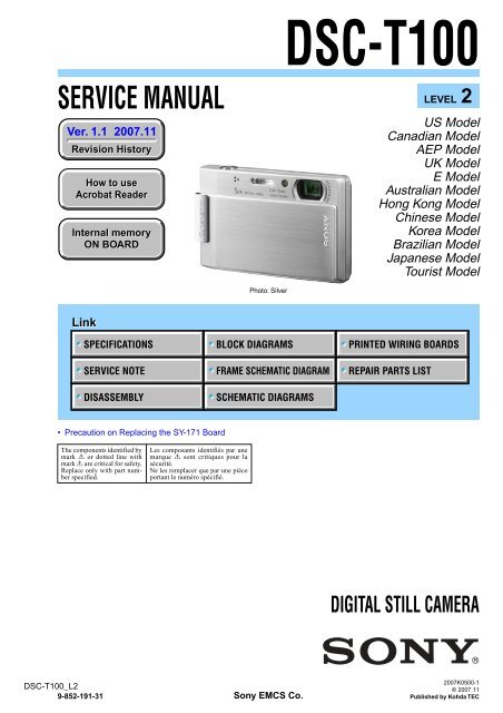
Photo: Silver<br />
BLOCK DIAGRAMS<br />
FRAME SCHEMATIC DIAGRAM<br />
SCHEMATIC DIAGRAMS<br />
<strong>Sony</strong> EMCS Co.<br />
<strong>DSC</strong>-<strong>T100</strong><br />
REPAIR PARTS LIST<br />
LEVEL 2<br />
US Model<br />
Canadian Model<br />
AEP Model<br />
UK Model<br />
E Model<br />
Australian Model<br />
Hong Kong Model<br />
Chinese Model<br />
Korea Model<br />
Brazilian Model<br />
Japanese Model<br />
Tourist Model<br />
PRINTED WIRING BOARDS<br />
DIGITAL STILL CAMERA<br />
2007K0500-1<br />
© 2007.11<br />
Published by Kohda TEC
<strong>Camera</strong><br />
[System]<br />
Image device: 7.18 mm (1/2.5 type) color CCD,<br />
Primary color filter<br />
Total pixel number <strong>of</strong> camera:<br />
Approx. 8 286 000 pixels<br />
Effective pixel number <strong>of</strong> camera:<br />
Approx. 8 083 000 pixels<br />
Lens: Carl Zeiss Vario-Tessar 5 × zoom lens f =<br />
5.8 − 29.0 mm (35 − 175mm when converted<br />
to a 35 mm still camera) F3.5 − 4.4<br />
Exposure control: Automatic exposure, Scene<br />
Selection (9 modes)<br />
White balance: Automatic, Daylight, Cloudy,<br />
Fluorescent 1, Fluorescent 2, Fluorescent 3,<br />
Incandescent, Flash<br />
File format (DCF compliant):<br />
Still images: Exif Ver. 2.21 JPEG compliant,<br />
DPOF compatible<br />
Movies: MPEG1 compliant (Monaural)<br />
Recording media: Internal Memory (approx.<br />
31 MB), “Memory Stick Duo”<br />
Flash: Flash range (ISO (Recommended Exposure<br />
Index) set to Auto): approx. 0.1 to 3.7 m<br />
(4 inches to 12 feet 1 3/4 inches) (W)/<br />
approx. 0.8 to 2.9 m (2 feet 7 1/2 inches to<br />
9feet 6 1/4 inches) (T)<br />
<strong>DSC</strong>-<strong>T100</strong>_L2<br />
SPECIFICATIONS<br />
[Input and Output connectors]<br />
Multi connector:<br />
Video output<br />
Audio output (mono)<br />
USB communication<br />
USB communication:<br />
Hi-Speed USB (USB 2.0 compliant)<br />
[LCD screen]<br />
LCD panel: 7.5 cm (3.0 type) TFT drive<br />
Total number <strong>of</strong> dots: 230 400 (960 × 240) dots<br />
[Power, general]<br />
Power:<br />
Rechargeable battery pack NP-BG1, 3.6 V<br />
AC-LS5K AC Adaptor (not supplied), 4.2 V<br />
Power consumption (during shooting): 1.1 W<br />
Operating temperature: 0 to 40°C (32 to 104°F)<br />
Storage temperature: −20 to +60°C (–4 to +140°F)<br />
Dimensions: 91.85 × 9.2 × 22.3mm<br />
(3 5/8 × 2 3/8 × 29/32inches)<br />
(W/H/D, excluding protrusions)<br />
Mass: Approx. 172 g (6.1 oz) (including NP-BG1<br />
battery pack and wrist strap, etc.)<br />
Microphone: Monaural<br />
Speaker: Monaural<br />
Exif Print: Compatible<br />
PRINT Image Matching III: Compatible<br />
PictBridge: Compatible<br />
— 2 —<br />
BC-CSG/BC-CSGB/BC-CSGC<br />
battery charger<br />
Power requirements: AC 100 to 240 V, 50/60 Hz,<br />
2W (BC-CSG/BC-CSGC)/ 2.6 W (BC-<br />
CSGB)<br />
Output voltage: DC 4.2 V, 0.25 A<br />
Operating temperature: 0 to 40°C (32 to 104°F)<br />
Storage temperature: -20 to +60°C (−4 to<br />
+140°F)<br />
Dimensions: Approx. 62 × 24 × 91mm (2 1/2 ×<br />
31/32 × 3 5/8 inches) (W/H/D)<br />
Mass: Approx. 75 g (2.7 oz)<br />
Rechargeable battery pack NP-<br />
BG1<br />
Used battery: Lithium-ion battery<br />
Maximum voltage: DC 4.2 V<br />
Nominal voltage: DC 3.6 V<br />
Capacity: 3.4 Wh (960 mAh)<br />
Design and specifications are subject to change<br />
without notice.
<strong>DSC</strong>-<strong>T100</strong>_L2<br />
CAUTION<br />
Danger <strong>of</strong> explosion if battery is incorrectly replaced.<br />
Replace only with the same or equivalent type.<br />
SAFETY-RELATED COMPONENT WARNING!!<br />
COMPONENTS IDENTIFIED BY MARK 0 OR DOTTED LINE WITH<br />
MARK 0 ON THE SCHEMATIC DIAGRAMS AND IN THE PARTS<br />
LIST ARE CRITICAL TO SAFE OPERATION. REPLACE THESE<br />
COMPONENTS WITH SONY PARTS WHOSE PART NUMBERS<br />
APPEAR AS SHOWN IN THIS MANUAL OR IN SUPPLEMENTS<br />
PUBLISHED BY SONY.<br />
1. Check the area <strong>of</strong> your repair for unsoldered or poorly-soldered<br />
connections. Check the entire board surface for solder splashes<br />
and bridges.<br />
2. Check the interboard wiring to ensure that no wires are<br />
"pinched" or contact high-wattage resistors.<br />
3. Look for unauthorized replacement parts, particularly<br />
transistors, that were installed during a previous repair. Point<br />
them out to the customer and recommend their replacement.<br />
4. Look for parts which, through functioning, show obvious signs<br />
<strong>of</strong> deterioration. Point them out to the customer and<br />
recommend their replacement.<br />
5. Check the B+ voltage to see it is at the values specified.<br />
6. FLEXIBLE Circuit Board Repairing<br />
• Keep the temperature <strong>of</strong> the soldering iron around 270°C<br />
during repairing.<br />
• Do not touch the soldering iron on the same conductor <strong>of</strong> the<br />
circuit board (within 3 times).<br />
• Be careful not to apply force on the conductor when soldering<br />
or unsoldering.<br />
SAFETY CHECK-OUT<br />
After correcting the original service problem, perform the following<br />
safety checks before releasing the set to the customer.<br />
— 3 —<br />
ATTENTION AU COMPOSANT AYANT RAPPORT<br />
À LA SÉCURITÉ!<br />
LES COMPOSANTS IDENTIFÉS PAR UNE MARQUE 0 SUR LES<br />
DIAGRAMMES SCHÉMATIQUES ET LA LISTE DES PIÈCES SONT<br />
CRITIQUES POUR LA SÉCURITÉ DE FONCTIONNEMENT. NE<br />
REMPLACER CES COMPOSANTS QUE PAR DES PIÈSES SONY<br />
DONT LES NUMÉROS SONT DONNÉS DANS CE MANUEL OU<br />
DANS LES SUPPÉMENTS PUBLIÉS PAR SONY.<br />
Unleaded solder<br />
Boards requiring use <strong>of</strong> unleaded solder are printed with the leadfree<br />
mark (LF) indicating the solder contains no lead.<br />
(Caution: Some printed circuit boards may not come printed with<br />
the lead free mark due to their particular size.)<br />
: LEAD FREE MARK<br />
Unleaded solder has the following characteristics.<br />
• Unleaded solder melts at a temperature about 40°C higher than<br />
ordinary solder.<br />
Ordinary soldering irons can be used but the iron tip has to be<br />
applied to the solder joint for a slightly longer time.<br />
Soldering irons using a temperature regulator should be set to<br />
about 350°C.<br />
Caution: The printed pattern (copper foil) may peel away if the<br />
heated tip is applied for too long, so be careful!<br />
• Strong viscosity<br />
Unleaded solder is more viscous (sticky, less prone to flow) than<br />
ordinary solder so use caution not to let solder bridges occur such<br />
as on IC pins, etc.<br />
• Usable with ordinary solder<br />
It is best to use only unleaded solder but unleaded solder may<br />
also be added to ordinary solder.
Section<br />
TABLE OF CONTENTS<br />
Title Page<br />
1. SERVICE NOTE<br />
1-1. Precaution on Replacing the SY-171 Board ····················1-1<br />
1-2. Self-diagnosis Function ···················································1-1<br />
1-3. Process After Fixing Flash Error ·····································1-2<br />
1-4. Method for Copying or Erasing the Data in Internal<br />
Memory ···········································································1-3<br />
1-5. How to Write Data to Internal Memory ··························1-4<br />
2. DISASSEMBLY<br />
2-1. Disassembly·····································································2-2<br />
3. BLOCK DIAGRAMS<br />
3-1. Overall Block Diagram (1/2) ···········································3-1<br />
3-2. Overall Block Diagram (2/2) ···········································3-2<br />
3-3. Power Block Diagram (1/2)·············································3-3<br />
3-4. Power Block Diagram (2/2)·············································3-4<br />
4. PRINTED WIRING BOARDS AND<br />
SCHEMATIC DIAGRAMS<br />
4-1. Frame Schematic Diagram ··············································4-1<br />
4-2. Schematic Diagrams ························································4-3<br />
4-3. Printed Wiring Boards ···················································4-19<br />
5. REPAIR PARTS LIST<br />
5-1. Exploded Views ·······························································5-2<br />
5-2. Electrical Parts List ·························································5-5<br />
<strong>DSC</strong>-<strong>T100</strong>_L2<br />
— 4 —
<strong>DSC</strong>-<strong>T100</strong>_L2<br />
1-2. SELF-DIAGNOSIS FUNCTION<br />
1-2-1. Self-diagnosis Function<br />
When problems occur while the unit is operating, the self-diagnosis<br />
function starts working, and displays on the LCD screen what to<br />
do.<br />
Details <strong>of</strong> the self-diagnosis functions are provided in the Instruction<br />
manual.<br />
C<br />
3 2<br />
1. SERVICE NOTE<br />
1-1. PRECAUTION ON REPLACING THE SY-171 BOARD<br />
DESTINATION DATA<br />
When you replace to the repairing board, the written destination data <strong>of</strong> repairing board also might be changed to original setting.<br />
Refer to <strong>Service</strong> <strong>Manual</strong> ADJ, and perform “DESTINATION DATA WRITE”.<br />
USB SERIAL No.<br />
The set is shipped with a unique ID (USB Serial No.) written in it.<br />
This ID has not been written in a new board for service, and therefore it must be entered after the board replacement.<br />
Refer to <strong>Service</strong> <strong>Manual</strong> ADJ, and perform “USB SERIAL No. INPUT”.<br />
LCD screen<br />
Blinks at 3.2 Hz<br />
0 0<br />
Repaired by:<br />
Block Detailed Code<br />
C : Corrected by customer<br />
E : Corrected by service<br />
engineer<br />
Indicates the appropriate<br />
step to be taken.<br />
E.g.<br />
Refer to “1-2-3. Self-diagnosis Code Table”.<br />
13 ....Format the “Memory Stick Duo”.<br />
32 ....Turn on power again.<br />
1-1<br />
1-2-2. Self-diagnosis Display<br />
When problems occur while the unit is operating, the LCD screen<br />
shows a 4-digit display consisting <strong>of</strong> an alphabet and numbers, which<br />
blinks at 3.2 Hz. This 5-character display indicates the “repaired<br />
by:”, “block” in which the problem occurred, and “detailed code”<br />
<strong>of</strong> the problem.
1-2-3. Self-diagnosis Code Table<br />
Repaired by:<br />
C<br />
C<br />
E<br />
E<br />
E<br />
E<br />
E<br />
E<br />
E<br />
E<br />
E<br />
Self-diagnosis Code<br />
Block<br />
Function<br />
1 3<br />
3 2<br />
6 1<br />
6 1<br />
6 2<br />
6 2<br />
6 2<br />
6 2<br />
6 2<br />
9 1<br />
9 2<br />
1-3. PROCESS AFTER FIXING FLASH ERROR<br />
When “FLASH error” (Self-diagnosis Code E : 91 : 01) occurs, to prevent any abnormal situation caused by high voltage, setting <strong>of</strong> the flash<br />
is changed automatically to disabling charge and flash setting.<br />
After fixing, this setting needs to be deactivated. Flash error code can be initialized by the operations on the HOME screen.<br />
Method for Initializing the Flash Error Code<br />
<strong>DSC</strong>-<strong>T100</strong>_L2<br />
Detailed<br />
Code<br />
0 1<br />
0 1<br />
0 0<br />
1 0<br />
0 2<br />
1 0<br />
1 1<br />
1 2<br />
2 0<br />
0 1<br />
0 0<br />
Symptom/State<br />
The internal memory has experienced a<br />
format error.<br />
“Memory Stick Duo” is unformatted.<br />
“Memory Stick Duo” is broken.<br />
“Memory Stick Duo” type error<br />
The camera cannot read or write data<br />
on the “Memory Stick Duo”.<br />
Trouble with hardware<br />
Difficult to adjust focus<br />
(Cannot initialize focus)<br />
Zoom operations fault<br />
(Cannot initialize zoom lens.)<br />
Abnormality <strong>of</strong> IC for steadyshot.<br />
Lens initializing failure.<br />
Lens overheating (PITCH).<br />
Lens overheating (YAW).<br />
Abnormality <strong>of</strong> thermistor.<br />
Abnormality when flash is being charged.<br />
Non-standard battery is used.<br />
1-2<br />
Format the internal memory.<br />
Note: After repair, be sure to perform “1-3. PROCESS AFTER FIXING FLASH ERROR”.<br />
Initialize<br />
Initializes the setting to the default setting. The images stored in the internal memory are<br />
retained.<br />
1 Select [Initialize] with v/V/b/B, then press z.<br />
The message “Initialize all settings” appears.<br />
2 Select [OK] with v, then press z.<br />
The settings are reset to the default setting.<br />
To cancel the resetting<br />
Select [Cancel] in step 2, then press z.<br />
• Make sure that the power is not disconnected during resetting.<br />
Correction<br />
Format the “Memory Stick Duo”.<br />
Insert a new “Memory Stick Duo”.<br />
Insert a supported “Memory Stick Duo”.<br />
Turn the power <strong>of</strong>f and on again, or taking out and inserting the<br />
“Memory Stick Duo” several times.<br />
Turn the power <strong>of</strong>f and on again.<br />
Retry turn the power on by the power switch. If it does not<br />
recover, check the focus reset sensor <strong>of</strong> lens block (pin 6 <strong>of</strong><br />
CN402 on the SY-171 board). If it is OK, check the focus motor<br />
drive IC (IC401 on the SY-171 board).<br />
Retry turn the power on by the power switch. Check the zoom<br />
reset sensor <strong>of</strong> lens block (pin 9 <strong>of</strong> CN402 on the SY-171<br />
board) when zooming is performed when the zoom button is<br />
operated. If it is OK, check the zoom motor drive IC (IC401 on<br />
the SY-171 board).<br />
Check or replacement <strong>of</strong> the IC for steadyshot (IC503 on the SY-<br />
171 board).<br />
Check or replacement <strong>of</strong> the IC for steadyshot (IC503 on the SY-<br />
171 board).<br />
Check the HALL element (PITCH) <strong>of</strong> optical image stabilizer<br />
(pin ea, es <strong>of</strong> CN402 on the SY-171 board). If it is OK, check<br />
PITCH angular velocity sensor (SE502 on the SY-171 board)<br />
peripheral circuits.<br />
Check the HALL element (YAW) <strong>of</strong> optical image stabilizer (pin<br />
ed, ef <strong>of</strong> CN402 on the SY-171 board). If it is OK, check YAW<br />
angular velocity sensor (SE501 on the SY-171 board) peripheral<br />
circuits.<br />
Check the OIS temp sensor <strong>of</strong> optical image stabilizer (pin wa <strong>of</strong><br />
CN402 on the SY-171 board).<br />
Checking <strong>of</strong> flash unit or replacement <strong>of</strong> flash unit. (Note)<br />
Use the compatible battery only.
<strong>DSC</strong>-<strong>T100</strong>_L2<br />
1-4. METHOD FOR COPYING OR ERASING THE DATA IN INTERNAL MEMORY<br />
The data can be copied/erased by the operations on the HOME screen. (When erasing the data, execute formatting the internal memory.)<br />
Note 1: When replacing the SY-171 board, erase the data in internal memory <strong>of</strong> the board before replacement.<br />
Note 2: When replacing the SY-171 board, execute formatting and initialize the internal memory after replacement.<br />
Method for Copying the Data in Internal Memory<br />
Copy<br />
Copies all images in the internal memory to a “Memory Stick Duo”.<br />
1 Insert a “Memory Stick Duo” having 32MB or larger capacity.<br />
2 Select [Copy] with v/V/b/B on the control button, then press z.<br />
The message “All data in internal memory will be copied” appears.<br />
3 Select [OK] with v, then press z.<br />
Copying starts.<br />
To cancel the copying<br />
Select [Cancel] in step 3, then press z.<br />
• Use a fully charged battery pack. If you attempt to copy image files using a battery pack with little<br />
remaining charge, the battery pack may run out, causing copying to fail or possibly corrupting the data.<br />
• You cannot copy individual images.<br />
• The original images in the internal memory are retained even after copying. To delete the contents <strong>of</strong> the<br />
internal memory, remove the “Memory Stick Duo” after copying, then execute the [Format] command in<br />
[ Internal Memory Tool].<br />
• When you copy the data in the internal memory to the “Memory Stick Duo”, all the data will be copied.<br />
You cannot choose a specific folder on the “Memory Stick Duo” as the destination for the data to be<br />
copied.<br />
• Even if you copy data, a DPOF (Print order) mark is not copied.<br />
Method for Formatting the Internal Memory<br />
This item does not appear when a “Memory Stick Duo” is inserted in the camera.<br />
Format<br />
Formats the internal memory.<br />
• Note that formatting irrevocably erases all data in the internal memory, including even protected images.<br />
1 Select [Format] with v/V/b/B on the control button, then press z.<br />
The message “All data in internal memory will be erased” appears.<br />
2 Select [OK] with v, then press z.<br />
The format is complete.<br />
To cancel the formatting<br />
Select [Cancel] in step 2, then press z.<br />
1-3
1-5. HOW TO WRITE DATA TO INTERNAL MEMORY<br />
Usually, the camera has been set so as to disable the data writing from the PC to the internal memory <strong>of</strong> the camera.<br />
This setting must be changed temporarily when the data is to be written to the internal memory such as a case after the board replacement.<br />
To change the setting, use the write enable tool “WriteEnableTool.exe”.<br />
Data writing method<br />
1) Connect the PC to the camera (USB mode: Mass Storage), and switch the driver to the “<strong>Sony</strong> Seus USB Driver”.<br />
2) Start the Write Enable Tool and the SeusEX.<br />
3) Click the [Activate Write Enable Mode] button <strong>of</strong> the Write Enable Tool.<br />
4) Upon completion <strong>of</strong> the setting change, the following message will be displayed.<br />
5) Return the driver to the original one, and connect the PC to the camera (USB mode: Mass Storage).<br />
6) Write the data read out into the PC to the internal memory <strong>of</strong> the camera.<br />
7) Disconnect the PC from the camera, and turn <strong>of</strong>f the camera.<br />
Note: By turning <strong>of</strong>f the camera, the write enable setting is reset.<br />
<strong>DSC</strong>-<strong>T100</strong>_L2<br />
1-4E
<strong>DSC</strong>-<strong>T100</strong>_L2<br />
NOTE FOR REPAIR<br />
2. DISASSEMBLY<br />
• Make sure that the flat cable and flexible board are not cracked <strong>of</strong> bent at the terminal.<br />
Do not insert the cable insufficiently nor crookedly.<br />
• When remove a connector, don’t pull at wire <strong>of</strong> connector. It is possible that a wire is snapped.<br />
• When installing a connector, don’t press down at wire <strong>of</strong> connector.<br />
It is possible that a wire is snapped.<br />
• Do not apply excessive load to the gilded flexible board.<br />
2-1<br />
Cut and remove the part <strong>of</strong> gilt<br />
which comes <strong>of</strong>f at the point.<br />
(Be careful or some<br />
pieces <strong>of</strong> gilt may be left inside)<br />
DISCHARGING OF THE ST-162 FLEXIBLE BOARD’S CHARGING CAPACITOR<br />
(C901)<br />
The charging capacitor (C901) <strong>of</strong> the ST-162 flexible board is<br />
charged up to the maximum 300 V potential.<br />
There is a danger <strong>of</strong> electric shock by this high voltage when the<br />
capacitor is handled by hand. The electric shock is caused by<br />
the charged voltage which is kept without discharging when the<br />
main power <strong>of</strong> the unit is simply turned <strong>of</strong>f. Therefore, the<br />
remaining voltage must be discharged as described below.<br />
Preparing the Short Jig<br />
To preparing the short jig, a small clip is attached to each end <strong>of</strong><br />
a resistor <strong>of</strong> 1 kΩ /1 W (1-215-869-11).<br />
Wrap insulating tape fully around the leads <strong>of</strong> the resistor to<br />
prevent electrical shock.<br />
1 kΩ/1 W<br />
Wrap insulating tape.<br />
Note: High-voltage cautions<br />
Discharging the Capacitor<br />
Short-circuit between the two points<br />
with the short jig about 10 seconds.<br />
C901<br />
R:1 kΩ/1 W<br />
(Part code: 1-215-869-11)
2-1. DISASSEMBLY<br />
2-1-1. FRONT CABINET/LENS SECTION<br />
Follow the disassembly in the numerical order given.<br />
1 Cabinet (Front) Assy (1-1 to 1-9)<br />
2 Lens Block (2-1 to 2-5)<br />
1-5<br />
(#20/#21)<br />
<strong>DSC</strong>-<strong>T100</strong>_L2<br />
1-7<br />
(#26)<br />
1 Cabinet (Front) Assy<br />
1-4<br />
(#20/#21)<br />
1-9<br />
(RED only)<br />
2-1<br />
1-2 (Claw)<br />
1-3<br />
1-1<br />
(#20/#21)<br />
2-2<br />
HELP<br />
EXPLODED VIEW HARDWARE LIST<br />
Note: High-voltage cautions<br />
Discharging the Capacitor<br />
Short-circuit between the two points<br />
with the short jig about 10 seconds.<br />
R:1 kΩ/1 W<br />
(Part code: 1-215-869-11)<br />
2-4<br />
(#26)<br />
1-8<br />
(#26)<br />
2-2<br />
2-3<br />
C901<br />
2-5<br />
1-6 (#26)<br />
2 Lens Block<br />
HELP<br />
HELP<br />
HELP
<strong>DSC</strong>-<strong>T100</strong>_L2<br />
2-1-2. LCD/MAIN BOARD SECTION<br />
Follow the disassembly in the numerical order given.<br />
1 SY-171 Board (1-1 to 1-9)<br />
2 Cabinet (Rear) Assy (2-1 to 2-2)<br />
3 LCD Panel Block (3-1 to 3-2)<br />
1 SY-171<br />
Board<br />
1-5<br />
(Claw)<br />
1-4<br />
(#71)<br />
1-9<br />
(Claw)<br />
SY-171<br />
1-6<br />
(Claw)<br />
3 LCD Panel Block<br />
1-1<br />
1-7<br />
1-2<br />
HELP<br />
3-2<br />
1-3<br />
2-2<br />
2-3<br />
EXPLODED VIEW HARDWARE LIST<br />
2 Cabinet (Rear) Assy<br />
3-1<br />
1-8<br />
(Claw)<br />
2-1<br />
(#20/#21)
2-1-3. BT HOLDER SECTION<br />
Follow the disassembly in the numerical order given.<br />
1 SW-496 Flexible Board (1-1 to 1-5)<br />
2 Flash Unit (2-1 to 2-4)<br />
3 BT-035 Flexible Board (3-1 to 3-3)<br />
2 Flash Unit<br />
<strong>DSC</strong>-<strong>T100</strong>_L2<br />
2-2<br />
3-2<br />
HELP<br />
2-1 (Claw)<br />
2-4 (Claw)<br />
3-1 (Solder)<br />
HELP<br />
2-4E<br />
1-5<br />
(Claw)<br />
EXPLODED VIEW HARDWARE LIST<br />
2-3<br />
(Claw)<br />
3-3<br />
3 BT-035 Flexible Board<br />
1-1<br />
(#26)<br />
1-2<br />
1-3<br />
(Claw)<br />
1-4<br />
1 SW-496<br />
Flexible<br />
Board
<strong>DSC</strong>-<strong>T100</strong>_L2<br />
HELP<br />
Sheet attachment positions and procedures <strong>of</strong> processing the flexible boards/harnesses are shown.<br />
Harness (Black)<br />
Microphone block<br />
Harness (Black)<br />
SY-171<br />
board<br />
SW-496 flexible board<br />
Loudspeaker<br />
Harness (Red)<br />
Harness (Red)<br />
HELP
PRECAUTIONS WHEN HOLDING THE LSV-1220A<br />
• Hold the LSV-1220A at the center <strong>of</strong> both sides. • Do not hold the LSV-1220A in the front-rear thickness<br />
direction.<br />
• Do not touch the top <strong>of</strong> lens prism. • Do not touch the motor coil or terminals.<br />
<strong>DSC</strong>-<strong>T100</strong>_L2<br />
LSV-1220A<br />
LSV-1220A<br />
Hold here.<br />
Do not touch here.<br />
Lens prism<br />
LSV-1220A<br />
LSV-1220A<br />
Motor<br />
Do not touch<br />
the coil.<br />
Do not touch<br />
the terminals.<br />
HELP
<strong>DSC</strong>-<strong>T100</strong>_L2<br />
FOCUS MOTOR DISASSEMBLING PROCEDURE<br />
Solder<br />
Note:<br />
Take care not to melt<br />
the mold part <strong>of</strong> .<br />
Screw<br />
Focus motor<br />
Lens block<br />
Lens<br />
Cover the lens surface for protection.<br />
1 Cover the lens surface to protect from solder splashing.<br />
2 Remove the solder.<br />
3 Remove one screw.<br />
* Tightening torque = 0.5 ± 0.1kgf • cm<br />
4 Remove the focus motor from the lens block.<br />
ZOOM MOTOR DISASSEMBLING PROCEDURE<br />
Screw<br />
Lens block<br />
Zoom motor<br />
Lens<br />
Cover the lens<br />
surface for protection.<br />
Note:<br />
Take care not to melt<br />
the mold part <strong>of</strong> .<br />
1 Cover the lens surface to protect from solder splashing.<br />
2 Remove the solder.<br />
3 Remove two screws.<br />
* Tightening torque = 0.5 ± 0.1kgf • cm<br />
4 Remove the zoom motor from the lens block.<br />
Solder<br />
HELP
INSTALLATION METHOD OF BATTERY TERMINAL BOARD<br />
1 Install the BT-035 flexible board in the BT holder.<br />
2 Insert the battery terminal board into a slit in the BT holder to install.<br />
*The battery terminal board is attached with the notch for installation.<br />
<strong>DSC</strong>-<strong>T100</strong>_L2<br />
BT holder<br />
2Battery terminal board<br />
3 Fold the notch 3 or 4 times repeatedly to break.<br />
Notch<br />
1BT-035<br />
flexible board<br />
Notch<br />
Notch<br />
Battery terminal<br />
board<br />
Battery terminal board<br />
HELP
<strong>DSC</strong>-<strong>T100</strong>_L2<br />
Link<br />
OVERALL BLOCK DIAGRAM (2/2)<br />
3. BLOCK DIAGRAMS<br />
OVERALL BLOCK DIAGRAM (1/2) POWER BLOCK DIAGRAM (1/2)<br />
POWER BLOCK DIAGRAM (2/2)
<strong>DSC</strong>-<strong>T100</strong>_L2<br />
3. BLOCK DIAGRAMS<br />
3-1. OVERALL BLOCK DIAGRAM (1/2) ( ) : Number in parenthesis ( ) indicates the division number <strong>of</strong> schematic diagram where the component is located.<br />
ZOOM<br />
RESET<br />
SENSOR<br />
LENS<br />
M901<br />
ZOOM<br />
MOTOR<br />
M<br />
LENS BLOCK<br />
FOCUS<br />
RESET<br />
SENSOR<br />
M902<br />
FOCUS<br />
MOTOR<br />
M<br />
OPTICAL IMAGE<br />
STABILIZER<br />
IRIS<br />
(METER)<br />
IRIS<br />
MOTOR<br />
M<br />
LENS TEMP<br />
SENSOR<br />
OIS TEMP<br />
SENSOR<br />
YAW<br />
MOTOR M<br />
HALL<br />
ELEMENT<br />
PITCH<br />
MOTOR M<br />
HALL<br />
ELEMENT<br />
CD-696 FLEXIBLE BOARD SY-171 BOARD (1/2)<br />
SW-496 FLEXIBLE<br />
BOARD (1/2)<br />
18 10 14 38<br />
CN301<br />
CCD_OUT<br />
D14<br />
IC001<br />
8.1M CCD<br />
IMAGER<br />
IC002<br />
BUFFER<br />
18<br />
POWER_SAVE<br />
C7<br />
28 - 30<br />
32, 33 16, 15<br />
1, 16<br />
13, 14 34, 33 21 - 32<br />
4 - 2<br />
27 6<br />
20 8<br />
3 - 14<br />
IRIS_A, A, B, B<br />
FOCUS_A, A, B, B<br />
ZOOM_A, A, B, B<br />
FC_SENS<br />
FC_SENS_GND<br />
ZM_SENS<br />
ZM_SENS_GND<br />
LENS_TEMP<br />
OIS_TEMP<br />
YAW±<br />
YAW_HALL_BIAS±,<br />
YAW_HALL±<br />
PITCH±<br />
PITCH_HALL_BIAS±,<br />
PITCH_HALL±<br />
31 12<br />
H1 - H3<br />
LH1<br />
RG<br />
V1, V2, V3A, V3B, V4,<br />
V5A, V5B, V6 - V10<br />
VST1, VST2<br />
VHLD1, VHLD2<br />
CA_FD<br />
XDD_SYS_RST<br />
CLK_IC_503<br />
XIC_211_IC_503_RST<br />
XCS_IC_503<br />
P10, P9, P11<br />
P7<br />
P8<br />
SUB<br />
1 19<br />
J4<br />
SUB_CONT<br />
25<br />
17<br />
05<br />
17 - 14<br />
1 - 4<br />
36 - 39<br />
6<br />
8<br />
9<br />
11<br />
12<br />
21<br />
18, 19, 26, 27<br />
22, 23, 33, 34<br />
20, 24, 25<br />
29 - 32<br />
CN402<br />
B10, D10<br />
G6, J8, J9, J7<br />
B1, D1<br />
J3, J2, H2, J4<br />
IC503<br />
OPTICAL<br />
IMAGE<br />
STABILIZATION<br />
DRIVE<br />
(3/11)<br />
J5<br />
LV<br />
D5, D6<br />
G5<br />
C9<br />
A7<br />
A3<br />
A6<br />
A5<br />
A4, B4, B5<br />
Q301<br />
SWAOUT<br />
CLK, DATA<br />
SWBOUT<br />
Q302<br />
13<br />
24, 25<br />
10<br />
IC506<br />
F1, G2, E2, E1,<br />
G1, D4, D3, F4,<br />
E4, F3, D1, C2<br />
J2, H4<br />
H3, H1<br />
G4<br />
C6<br />
F2, E2, D2, B1<br />
D6, E6, B7, C6<br />
B4, B5, B3, A3<br />
PITCH/YAW<br />
SENSOR<br />
AMP<br />
(3/11)<br />
IC304<br />
CCD SIGNAL<br />
PROCESS,<br />
TIMING<br />
GENERATOR<br />
(1/11)<br />
IC401<br />
LENS DRIVE<br />
(2/11)<br />
IRIS MOTOR<br />
DRIVER<br />
FOCUS<br />
MOTOR<br />
DRIVER<br />
ZOOM<br />
MOTOR<br />
DRIVER<br />
21<br />
1<br />
N5, P4, M4, N2, L3, L1, P5,<br />
L5, N4, N3, M2, L2, K4, K3<br />
K13<br />
J13<br />
K14<br />
D10<br />
D7 - D9<br />
D4<br />
F5, E5, D3, F1<br />
D5, A6, B6, C5<br />
A2, C3, C4, A1<br />
SE501<br />
YAW<br />
SENSOR<br />
SE502<br />
PITCH<br />
SENSOR<br />
X201<br />
36MHz<br />
2<br />
CA_AD00 - CA_AD13<br />
CA_HD<br />
CA_FD<br />
GEN_TG_CLK<br />
IC202<br />
CLOCK<br />
GENERATOR<br />
(4/11)<br />
VSUB_CONT_PRE,<br />
VSUB_CONT_POST<br />
3-1<br />
1<br />
3<br />
5<br />
XDD_SYS_RST<br />
XCS_FE, XIC_211_3_SCK, IC_211_3_SO<br />
XLENS_DRIVER_PS<br />
IRIS_DIR_A, IRIS_BRK_A,<br />
IRIS_DIR_B, IRIS_BRK_B<br />
FC_DIR_A, FC_DIR_B, FC_BRK_A<br />
ZM_DIR_A, ZM_DIR_B, ZM_BRK_A<br />
XDD_SYS_RST<br />
IC_211_0_SO, IC_211_0_SI, XIC_211_0_SCK<br />
FC_SENS<br />
XFC_RST_LED<br />
ZM_SENS_1ST<br />
XZM_RST_LED<br />
LENS_TEMP<br />
TZ_HALL_TEMP<br />
GEAR_ON<br />
GEN_SYS_CLK<br />
1<br />
OVERALL (2/2)<br />
(PAGE 3-2)<br />
AB21, AC21, AB20, AC20, AB19,<br />
AC19, AC18, AE21, AF21, AE20,<br />
AF20, AE19, AF19, AE18<br />
AE23<br />
AF22<br />
AF18<br />
Y13<br />
Y12<br />
V19, D19, C25<br />
R7, AF25<br />
H11<br />
W16, AD25, Y18, Y17<br />
W18, AB26, W17<br />
AB23, AC26, AA23<br />
Y10<br />
M8<br />
AD26<br />
J8<br />
AE3<br />
AF3<br />
W13<br />
H10<br />
U8<br />
IC211<br />
(1/2)<br />
CPU<br />
(4/11, 5/11)<br />
D17, B19, E17, A19,<br />
E16, A18, D16, A17<br />
Y1, AA1 E18, B23 B18, D18, B17<br />
U19<br />
V8<br />
AF8<br />
AE8<br />
AB13<br />
AF12<br />
AC12<br />
V7<br />
A13 - A15,<br />
B13 - B15<br />
IC_211_CVOUT<br />
VOUT_1<br />
VOUT_2<br />
XHD_EN<br />
IC_211_2_SO,<br />
XIC_211_2_SCK<br />
XCS_AUDIO<br />
IC_211_AUIN<br />
IC_211_AUOUT<br />
BUFFER<br />
E6, D5<br />
D6<br />
A6<br />
B6<br />
F3<br />
Q242 - Q244<br />
LCD_D0 - LCD_D7<br />
LCD_CK, LCD_HD, LCD_VD<br />
XCS_ PANEL<br />
XDD_SYS_RST<br />
IC_211_2_SO, XIC_211_2_SCK<br />
2<br />
OVERALL (2/2)<br />
(PAGE 3-2)<br />
IC602<br />
AUDIO/VIDEO<br />
AMP<br />
(7/11)<br />
Q241<br />
CLAMP<br />
V_LINE_OUT V_OUT<br />
40<br />
IC_211_YOUT HDY<br />
26<br />
IC_211_PBOUT<br />
HDPb<br />
25<br />
IC_211_PROUT HDPr<br />
24<br />
USB_DP, USB_DM D±<br />
3<br />
OVERALL (2/2)<br />
(PAGE 3-2)<br />
A3<br />
A1, C1<br />
E2<br />
F1<br />
MSX_BS, MSX_D0 - MSX_D3, MSX_CLK<br />
BL_L<br />
CN713<br />
(1/2)<br />
46 - 39<br />
37, 35, 34<br />
31<br />
30<br />
32, 33<br />
51<br />
AU_LINE_OUT AOUT_L<br />
39<br />
2<br />
29, 32<br />
BL_H<br />
BL_L<br />
MIC_SIG<br />
USB_VBUS USB_VBUS<br />
35<br />
CN704<br />
XMS_IN<br />
6<br />
2 - 5, 7, 8<br />
FP-636<br />
FLEXIBLE<br />
D0 - D7<br />
DCK, HD, VD<br />
XCS<br />
RESET<br />
SI, SCK<br />
SP±<br />
BOARD (1/2)<br />
CN710<br />
(MAGIC FLEXIBLE)<br />
MEMORY<br />
STICK<br />
DUO<br />
9<br />
7<br />
20<br />
22<br />
24<br />
17, 14<br />
11<br />
CN001<br />
6 - 13<br />
14 - 16<br />
19<br />
20<br />
18, 17<br />
MC-178<br />
BOARD<br />
(1/2)<br />
W001<br />
(1/2)<br />
16<br />
20<br />
24<br />
4<br />
2<br />
10, 12<br />
A : VIDEO SIGNAL<br />
A : AUDIO SIGNAL<br />
A : VIDEO/AUDIO SIGNAL<br />
1<br />
2<br />
6<br />
LCD901<br />
3.0 inch<br />
COLOR<br />
LCD<br />
UNIT<br />
D901<br />
BACKLIGHT<br />
MIC901<br />
SP901<br />
SPEAKER<br />
CN001<br />
(1/2)<br />
MULTI<br />
CONNECTOR
3-2. OVERALL BLOCK DIAGRAM (2/2) ( ) : Number in parenthesis ( ) indicates the division number <strong>of</strong> schematic diagram where the component is located.<br />
FLASH<br />
UNIT<br />
<strong>DSC</strong>-<strong>T100</strong>_L2<br />
ST-162 FLEXIBLE BOARD<br />
XE_H<br />
TRIGGER<br />
TRIGGER_GND<br />
XE_L<br />
Q001<br />
FLASH<br />
DRIVE<br />
C901<br />
CHARGING<br />
CAPACITOR<br />
+<br />
D001<br />
3<br />
SW-496 FLEXIBLE BOARD<br />
(2/2)<br />
S002<br />
POWER<br />
T001<br />
4 1<br />
S003<br />
N<br />
S001<br />
(SHUTTER)<br />
D003<br />
(POWER)<br />
2<br />
BT001<br />
LITHIUM<br />
BATTERY<br />
ST_UNREG<br />
15<br />
1, 2<br />
7<br />
D002<br />
SELF-TIMER/<br />
AF ILLUMINATOR<br />
S004 - S012<br />
FUNCTION<br />
KEY<br />
IC002<br />
FLASH<br />
CONTROL,<br />
CHARGE<br />
CONTROL<br />
14<br />
13<br />
12, 11<br />
4<br />
10<br />
9<br />
6<br />
4<br />
SY-171 BOARD (2/2)<br />
CN713<br />
(2/2)<br />
XPWR_ON<br />
8<br />
7<br />
DIRECT_PB<br />
XAE_LOCK_SW<br />
XSHUT_SW<br />
KEY_AD_1,<br />
KEY_AD_2<br />
XPWR_LED<br />
05<br />
CN701<br />
4<br />
14<br />
13<br />
12<br />
11<br />
1<br />
STRB_CHG<br />
XSTRB_FULL<br />
STB_CHG_CONT<br />
STRB_ON1<br />
3<br />
OVERALL (1/2)<br />
(PAGE 3-1)<br />
XAF_LED<br />
VL_3V<br />
IC103<br />
LENS BARRIER<br />
DETECT<br />
(8/11)<br />
D101<br />
2<br />
BATT_SENS<br />
XMS_IN<br />
USB_VBUS<br />
3<br />
2<br />
IC102<br />
BACK UP VCC<br />
(8/11)<br />
IC106<br />
RESET<br />
(8/11)<br />
Q704<br />
AF LED<br />
CONTROL<br />
XPWR_ON<br />
DIRECT_PB<br />
Q102<br />
BATTERY<br />
DETECT<br />
Q101<br />
X101<br />
32.768kHz<br />
1<br />
1<br />
OVERALL (1/2)<br />
(PAGE 3-1)<br />
5<br />
4<br />
B8 H8<br />
B7<br />
A8<br />
C6<br />
D8<br />
J5<br />
J4<br />
D7<br />
A9<br />
IC101<br />
FRONT<br />
CONTROL<br />
(8/11)<br />
D102<br />
XDD_SYS_RST<br />
IC_211_0_SO,<br />
IC_211_0_SI,<br />
XIC_211_0_SCK<br />
3-2<br />
F9<br />
B9<br />
A1<br />
B4<br />
E2<br />
D1, D2, E1<br />
XPWR_ON<br />
BATT_SENS<br />
BL_EN2<br />
ST_UNREG<br />
BATT_SENS<br />
CAM_13V<br />
CAM_-7.5V<br />
PANEL_6.4V<br />
TI_DD_5V<br />
MT_5.0V<br />
D_3.0V<br />
A_3.0V<br />
DDR_1.8V<br />
D_1.8V<br />
D_1.2V<br />
MS_VCC<br />
BL_H<br />
XPWR_OFF<br />
XIC_211_RST_REQ<br />
XDD_SYS_RST<br />
XCS_FR<br />
IC_211_0_SO,<br />
IC_211_0_SI,<br />
XIC_211_0_SCK<br />
D706<br />
(MS ACCESS)<br />
AFLED_CONT<br />
XPWR_LED<br />
XAE_LOCK_SW<br />
XSHUT_SW<br />
KEY_AD_1,<br />
KEY_AD_2<br />
STRB_CHG<br />
XSTRB_FULL<br />
STB_CHG_CONT<br />
STRB_ON1<br />
IC001<br />
DC/DC<br />
CONVERTER<br />
(9/11)<br />
Q006<br />
BACKLIGHT<br />
CONTROL<br />
G8 K8<br />
W12<br />
AB18<br />
G9<br />
A23<br />
H17, A24, G17<br />
H8<br />
G15<br />
Y9<br />
N19<br />
R19<br />
AC8, AF6<br />
V2<br />
H9<br />
H15<br />
Y16<br />
IC211<br />
(2/2)<br />
CPU<br />
(4/11, 5/11)<br />
D26, G19<br />
W20, H18, B24, G18<br />
BL_L<br />
2<br />
OVERALL (1/2)<br />
(PAGE 3-1)<br />
XACV_IN<br />
XAV_JACK_IN (XACC_IN)<br />
IC_211_1_UI, IC_211_1_UO<br />
XCS_IC_201,<br />
XIC_211_1_SCK,<br />
IC_211_1_SO,<br />
IC_211_1_SI<br />
XDD_SYS_RST<br />
B1, B5, C5, D5<br />
B2<br />
Q004,<br />
Q013<br />
D002<br />
D003<br />
IC201<br />
BATTERY<br />
AUTHENTICATION<br />
(11/11)<br />
E4<br />
FP-636 MC-178 BOARD<br />
FLEXIBLE<br />
BOARD (2/2)<br />
CN710<br />
(MAGIC FLEXIBLE)<br />
(2/2)<br />
W001<br />
10<br />
XPOWER_ON<br />
(2/2)<br />
37<br />
XPOWER_ON<br />
7<br />
19 - 22<br />
14 - 18<br />
36<br />
11, 12<br />
ACV_UNREG<br />
CHARGE_V<br />
JACK_IN<br />
UART_Rx,<br />
UART_Tx<br />
CN702<br />
1 - 5<br />
6<br />
7 - 10<br />
25 - 28<br />
29 - 33<br />
12<br />
35, 36<br />
ACV_UNREG<br />
CHARGE_V<br />
XAV_JACK_IN<br />
UART_Rx,<br />
UART_Tx<br />
BT-035 FLEXIBLE<br />
BOARD<br />
BATT_UNREG<br />
BATT_SIG<br />
BATT_GND<br />
23, 25<br />
XACV_DET BATT_XEXT<br />
13 34 19<br />
17, 21<br />
26<br />
15, 9<br />
+<br />
S<br />
–<br />
CN001<br />
(2/2)<br />
MULTI<br />
CONNECTOR<br />
BT901<br />
BATTERY<br />
TERMINAL
<strong>DSC</strong>-<strong>T100</strong>_L2<br />
3-3. POWER BLOCK DIAGRAM (1/2) ( ) : Number in parenthesis ( ) indicates the division number <strong>of</strong> schematic diagram where the component is located.<br />
CN001<br />
MULTI<br />
CONNECTOR<br />
BT901<br />
BATTERY<br />
TERMINAL<br />
+<br />
S<br />
–<br />
05<br />
23, 25<br />
MC-178<br />
BOARD<br />
W001<br />
ACV_UNREG<br />
BATT_XEXT XACV_DET<br />
19 34<br />
13<br />
17, 21<br />
CHARGE_V<br />
25-28<br />
29-33<br />
CN702<br />
19-22<br />
14-18<br />
SY-171 BOARD (1/2)<br />
ACV_UNREG<br />
CHARGE_V<br />
XPOWER_ON XPOWER_ON<br />
7 37 10<br />
BT-035 FLEXIBLE<br />
BOARD<br />
BATT_UNREG<br />
BATT_SIG<br />
BATT_GND<br />
A<br />
POWER (2/2)<br />
(PAGE 3-4)<br />
B<br />
POWER (2/2)<br />
(PAGE 3-4)<br />
C<br />
POWER (2/2)<br />
(PAGE 3-4)<br />
D<br />
POWER (2/2)<br />
(PAGE 3-4)<br />
FP-636 FLEXIBLE<br />
BOARD<br />
CN710<br />
(MAGIC FLEXIBLE)<br />
1-5<br />
6<br />
7-10<br />
XDD_SYS_RST<br />
XIC_211_RST_REQ<br />
XPWR_OFF<br />
XPWR_ON<br />
DIRECT_PB<br />
DDC2P9_EN<br />
D102<br />
D003<br />
D002<br />
IC201<br />
BATTERY<br />
AUTHENTICATION<br />
(11/11)<br />
B2 XRESET<br />
A9 CS<br />
B4 XSYS_RST<br />
IC101<br />
FRONT CONTROL<br />
(8/11)<br />
Q004, 013<br />
XACV_IN<br />
IC_211_1_SI<br />
P144_SOA0 D5<br />
E4 TXRX<br />
IC_211_1_SO<br />
P143_SIA0 C5<br />
XIC_211_1_SCK<br />
P142_XSCKA0 B5<br />
XCS_IC_201<br />
P120_INTP0 B1<br />
IC106<br />
RESET<br />
(8/11)<br />
1 OUT Vdd 4<br />
BATT_SENS H8<br />
DDC2P9_AD H7<br />
DDC1P8_AD J7<br />
DDC1P2_EN D9<br />
CAMDD_EN B2<br />
DDC2P9_EN E9<br />
BL_EN1 F8<br />
BL_EN2 F9<br />
DDC5PSW_EN F7<br />
VSU_EN J8<br />
A1 XRESET_REQ<br />
DDC1P8_EN E8<br />
B9 XPOWER_OFF<br />
DDC1P8_LVDET C9<br />
PANEL_EN B1<br />
EVER_PSB J9<br />
SW1P8_EN J1<br />
B8 XPOWER_ON0<br />
LDO1P8_EN H2<br />
B7 XPOWER_ON2<br />
DISW1P8_EN C2<br />
A8 XPOWER_ON1<br />
DISW2P9_EN C1<br />
XRSTX D7<br />
DDC1P2_RESET C8<br />
D_3.0V<br />
F001<br />
F002<br />
1.2V_INT<br />
E<br />
POWER (2/2)<br />
(PAGE 3-4)<br />
D_3.0V<br />
D_1.8V<br />
BACK_UP_VCC<br />
DDC1P2_EN<br />
CAMDD_EN<br />
DDC2P9_EN<br />
BL_EN1<br />
BL_EN2<br />
DDC5PSW_EN<br />
VSU_EN<br />
DDC1P8_EN<br />
DDCPV_EN<br />
PANEL_EN<br />
EVER_PSB<br />
SW_1P8_EN<br />
LDO_1P8_EN<br />
DISW1P8_EN<br />
DISW2P9_EN<br />
BATTERY<br />
DETECT<br />
L007<br />
Q102<br />
28 GD<br />
45 BATT<br />
13 PVSD<br />
29 PVBST<br />
35 PVLED<br />
47 LXSU<br />
9<br />
L002<br />
IC001<br />
DC/DC CONVERTER<br />
(9/11)<br />
PVAFE<br />
3-3<br />
LXSD 16<br />
ONSD 15<br />
LXBST 31<br />
SWBST 30<br />
ONBST 22<br />
LXINV 21<br />
PVINV 20<br />
ONINV 1<br />
PVM 4<br />
LXM 5<br />
ONM 3<br />
LXLED 33<br />
SWLED 34<br />
FBLLED 37<br />
ONLED 36<br />
SU 43<br />
PVSU 44<br />
ONSU 46<br />
SEQCCD 27<br />
LXAFE 8<br />
ONAFE 10<br />
IC002<br />
5V REG<br />
(9/11)<br />
9<br />
6<br />
SW<br />
VBAT<br />
VOUT 2<br />
7 LBI<br />
1 EN PS 8<br />
L009<br />
D011<br />
L004<br />
DDC1P2_EN<br />
CAMDD_EN<br />
L005<br />
DDC2P9_EN<br />
L003<br />
BL_EN1<br />
VSU_EN<br />
L006<br />
DDC1P8_EN<br />
EVER_PSB<br />
BL_EN2<br />
D007<br />
D010<br />
D006<br />
DDC5PSW_EN<br />
DDCPV_EN<br />
PANEL_EN<br />
SW_1P8_EN<br />
Q006<br />
BACKLIGHT<br />
CONTROL<br />
Q003<br />
B+ SWITCH<br />
Q014<br />
B+ SWITCH<br />
IC003<br />
1.8V REG<br />
(9/11)<br />
B2 VIN VOUT B1<br />
STBY<br />
A2<br />
LDO_1P8_EN<br />
DISW1P8_EN<br />
DISW2P9_EN<br />
D008, D009,<br />
C023, C025<br />
CHARGE<br />
PUMP<br />
CIRCUIT<br />
D_3.0V<br />
D_1.8V<br />
Q010, 012<br />
B+ SWITCH<br />
BACK_UP_VCC<br />
D101<br />
Q001<br />
B+ SWITCH<br />
IC102<br />
IC006<br />
6.4V REG<br />
(9/11)<br />
6 Vin Vout 4<br />
Vcont<br />
1<br />
BACK UP VCC<br />
(8/11)<br />
2 VCH<br />
3 VBAT VOUT 6<br />
7 VIN VRO 8<br />
5 XRESET<br />
4 CS<br />
MS_PWR_ON<br />
Q007<br />
1.8V/3.0V<br />
DISCHARGE<br />
F<br />
POWER (2/2)<br />
(PAGE 3-4)<br />
EVER_3V<br />
IC007<br />
VOLTAGE<br />
DETECTOR<br />
(9/11)<br />
VIN 4<br />
1 VOUT<br />
VSEN 3<br />
MS_VCC<br />
L001<br />
ST_UNREG<br />
IC103<br />
9<br />
D_1.2V<br />
CAM_13V<br />
CAM_-7.5V<br />
A_3.0V<br />
D_3.0V<br />
BL_H<br />
BL_L<br />
MT_5.0V<br />
PANEL_6.4V<br />
TI_DD_5V<br />
D_1.8V<br />
DDR_1.8V<br />
VL_3V<br />
LENS BARRIER<br />
DETECT<br />
(8/11)<br />
2 OUT<br />
CN704<br />
MEMORY<br />
STICK<br />
DUO<br />
G<br />
POWER (2/2)<br />
(PAGE 3-4)
3-4. POWER BLOCK DIAGRAM (2/2) ( ) : Number in parenthesis ( ) indicates the division number <strong>of</strong> schematic diagram where the component is located.<br />
05<br />
<strong>DSC</strong>-<strong>T100</strong>_L2<br />
SY-171 BOARD (2/2)<br />
G<br />
POWER (1/2)<br />
(PAGE 3-3)<br />
ST_UNREG<br />
D_1.2V<br />
CAM_13V<br />
CAM_-7.5V<br />
A_3.0V<br />
D_3.0V<br />
BL_H<br />
BL_L<br />
MT_5.0V<br />
PANEL_6.4V<br />
TI_DD_5V<br />
D_1.8V<br />
DDR_1.8V<br />
VL_3V<br />
B<br />
POWER (1/2)<br />
(PAGE 3-3)<br />
E<br />
POWER (1/2)<br />
(PAGE 3-3)<br />
F<br />
POWER (1/2)<br />
(PAGE 3-3)<br />
XACV_IN<br />
A_3.0V<br />
D_1.8V<br />
D_3.0V<br />
MT_5.0V<br />
D_1.8V<br />
D_3.0V<br />
TI_DD_5V<br />
MT_5.0V<br />
A_3.0V<br />
D_3.0V<br />
D_1.2V<br />
DDR_1.8V<br />
D_1.8V<br />
XIC_211_RST_REQ<br />
XPWR_OFF<br />
IC_211_1_SI<br />
IC_211_1_SO<br />
XIC_211_1_SCK<br />
XCS_IC_201<br />
MS_PWR_ON<br />
A<br />
POWER (1/2)<br />
(PAGE 3-3)<br />
IC501<br />
2.8V REG<br />
(3/11)<br />
B2 VIN VOUT B1<br />
VCONT<br />
A2<br />
L602<br />
R254<br />
IC502<br />
1.5V REG<br />
(3/11)<br />
B2 VIN VOUT B1<br />
XDD_SYS_RST<br />
XIC_211_IC_503_RST<br />
R253<br />
FB290<br />
L241<br />
FB281<br />
FB201<br />
FB282<br />
FB283<br />
H10 GPE_09<br />
AB18 XRESET<br />
XDD_SYS_RST<br />
IC211<br />
CPU<br />
(4/11)<br />
(5/11)<br />
(6/11)<br />
W12 XRESET_REQ<br />
G8 GPE_00<br />
K8 GPE_05<br />
G18 SIO1_RXD<br />
B24 SIO1_TXD<br />
H18 SIO1_SCK<br />
W20 GPS_04<br />
T7 GPE_15<br />
AU_AVCC<br />
TPU2_OUT G15<br />
IC503<br />
OPTICAL<br />
IMAGE<br />
STABILIZATION<br />
DRIVE<br />
(3/11)<br />
A7 RESET_N<br />
A6 XDL<br />
L211<br />
D_3.0V<br />
D_1.8V<br />
L601<br />
D601<br />
D602<br />
D_1.8V<br />
D_3.0V<br />
TI_DD_5V<br />
MT_5.0V<br />
AFLED_CONT<br />
CAM_3.5V<br />
D<br />
POWER (1/2)<br />
(PAGE 3-3)<br />
IC506<br />
PITCH/YAW<br />
SENSOR AMP<br />
(3/11)<br />
SE502<br />
PITCH<br />
SENSOR<br />
SE501<br />
YAW<br />
SENSOR<br />
IC602<br />
AUDIO/VIDEO<br />
AMP<br />
(7/11)<br />
D706<br />
(MS ACCESS)<br />
IC202<br />
CLOCK<br />
GENERATOR<br />
(4/11)<br />
DDC2P9_EN<br />
3-4E<br />
D_1.8V<br />
D_3.0V<br />
XDD_SYS_RST<br />
TI_DD_5V<br />
MT_5.0V<br />
TI_DD_5V<br />
D_3.0V<br />
XDD_SYS_RST<br />
D_3.0V<br />
MT_5.0V<br />
IC307<br />
3.5V REG<br />
(1/11)<br />
B2 VIN VOUT B1<br />
STBY<br />
A2<br />
IC306<br />
2.3V REG<br />
(1/11)<br />
B2 VIN VOUT B1<br />
6 Vin Vout 4<br />
IC308<br />
2.8V REG<br />
(1/11)<br />
PANEL_6.4V<br />
BL_H<br />
BL_L<br />
ST_UNREG<br />
VL_3V<br />
CAM_13V<br />
CAM_-7.5V<br />
Q704<br />
IC305<br />
13V REG<br />
(1/11)<br />
5 Vin Vout 4<br />
CAM_3.5V<br />
FB301<br />
FB303<br />
Q304<br />
2.8V/3.5V<br />
DISCHARGE<br />
C<br />
POWER (1/2)<br />
(PAGE 3-3)<br />
L701<br />
L702<br />
Q710<br />
AF LED<br />
DRIVE<br />
AF LED<br />
CONTROL<br />
FB302<br />
IC304<br />
CCD SIGNAL<br />
PROCESS,<br />
TIMING GENERATOR<br />
(1/11)<br />
D10 RESET<br />
ST_UNREG<br />
CN713<br />
VCCI<br />
VCC2(6V)<br />
VCC(3V)<br />
RESET<br />
BL_H<br />
BL_L<br />
D_3.0V<br />
XPWR_ON<br />
DIRECT_PB<br />
CN701<br />
M_5V<br />
M_5V<br />
XAF_LED<br />
VL_3V<br />
8, 9 23, 24 25, 26 27, 28<br />
30<br />
50<br />
51<br />
5<br />
8<br />
7<br />
10<br />
2<br />
1<br />
4<br />
SW-496 FLEXIBLE<br />
BOARD<br />
D003<br />
(POWER)<br />
S002<br />
POWER<br />
S003<br />
ST-162 FLEXIBLE BOARD<br />
D002<br />
SELF TIMER/<br />
AF ILLUMINATOR<br />
BT001<br />
LITHIUM<br />
BATTERY<br />
L303<br />
L302<br />
Q303<br />
-7.5V<br />
DISCHARGE<br />
CN402<br />
ZM_SENS_VCC<br />
10<br />
FC_SENS_VCC<br />
IC401<br />
LENS DRIVE<br />
(2/11)<br />
L001<br />
IC002<br />
FLASH CONTROL,<br />
CHARGE CONTROL<br />
T001<br />
LENS BLOCK<br />
ZOOM<br />
RESET<br />
SENSOR<br />
FOCUS<br />
RESET<br />
SENSOR<br />
D001<br />
CN301<br />
CD-696 FLEXIBLE<br />
BOARD<br />
CAM_13V<br />
15<br />
IC001<br />
CAM_-7.5V<br />
CN001<br />
VCCI<br />
36<br />
VCC2(6V)<br />
VCC(3V)<br />
RESET<br />
BL_H<br />
BL_L<br />
16<br />
7<br />
37<br />
38<br />
20<br />
1<br />
2<br />
LCD901<br />
3.0 inch<br />
COLOR<br />
LCD UNIT<br />
D901<br />
BACKLIGHT<br />
8.1M<br />
CCD IMAGER<br />
IC002<br />
BUFFER<br />
FLASH<br />
UNIT
<strong>DSC</strong>-<strong>T100</strong>_L2<br />
4-1. FRAME SCHEMATIC DIAGRAM<br />
BT901<br />
BATTERY<br />
TERMINAL<br />
BT-035 FLEXIBLE<br />
BOARD<br />
1<br />
10<br />
LEVEL3<br />
SY-171 BOARD<br />
(SIDE B)<br />
10 1<br />
CN702<br />
1 10<br />
SP901<br />
SPEAKER<br />
28<br />
CN704<br />
MEMORY STICK<br />
CONNECTOR<br />
26<br />
25<br />
CN001<br />
MULTI CONNECTOR<br />
2<br />
27<br />
4. PRINTED WIRING BOARDS AND SCHEMATIC DIAGRAMS<br />
12<br />
11<br />
LEVEL3<br />
MC-178 BOARD<br />
(SIDE B)<br />
1<br />
2 CN001 38<br />
1 39<br />
SW-496<br />
FLEXIBLE<br />
BOARD<br />
51<br />
51<br />
50<br />
9<br />
1-6 7<br />
8<br />
CN713<br />
IC211<br />
(Not supplied)<br />
LEVEL3<br />
FP-636 FLEXIBLE<br />
BOARD<br />
CN710 (MAGIC FLEXIBLE)<br />
1<br />
2<br />
1<br />
40<br />
38 41-46<br />
39<br />
40 38<br />
41-46 7<br />
8<br />
9 1-6<br />
39 W001<br />
LEVEL3<br />
MC-178 BOARD<br />
(SIDE A)<br />
4-1<br />
LCD901<br />
3.0 inch<br />
COLOR<br />
LCD UNIT<br />
D901<br />
BACKLIGHT<br />
MIC901<br />
MICROPHONE<br />
BLOCK<br />
LEVEL3<br />
SY-171 BOARD<br />
(SIDE A)<br />
2 38<br />
CN301<br />
1 39<br />
2 38<br />
CN402<br />
1 39<br />
1 14<br />
CN701<br />
39<br />
1<br />
IC001<br />
(Not supplied)<br />
IC002<br />
(Not supplied)<br />
LEVEL3<br />
CD-696 FLEXIBLE<br />
BOARD<br />
14<br />
1<br />
LENS BLOCK<br />
FLASH UNIT<br />
ST-162 FLEXIBLE BOARD<br />
BT001<br />
LITHIUM BATTERY<br />
C901<br />
CHARGING CAPACITOR<br />
FRAME
<strong>DSC</strong>-<strong>T100</strong>_L2<br />
Link<br />
SW-496 FLEXIBLE BOARD<br />
(LCD, CONTROL SWITCH)<br />
4-2. SCHEMATIC DIAGRAMS<br />
ST-162 FLEXIBLE BOARD (FLASH DRIVE)<br />
COMMON NOTE FOR SCHEMATIC DIAGRAMS<br />
BT-035 FLEXIBLE BOARD (BATTERY IN)
<strong>DSC</strong>-<strong>T100</strong>_L2<br />
4-2. SCHEMATIC DIAGRAMS<br />
4-2. SCHEMATIC DIAGRAMS<br />
THIS NOTE IS COMMON FOR SCHEMATIC DIAGRAMS<br />
(In addition to this, the necessary note is printed in each block)<br />
(For schematic diagrams)<br />
• All capacitors are in µF unless otherwise noted. pF : µ<br />
µF. 50 V or less are not indicated except for electrolytics<br />
and tantalums.<br />
• Chip resistors are 1/10 W unless otherwise noted.<br />
kΩ=1000 Ω, MΩ=1000 kΩ.<br />
• Caution when replacing chip parts.<br />
New parts must be attached after removal <strong>of</strong> chip.<br />
Be careful not to heat the minus side <strong>of</strong> tantalum<br />
capacitor, Because it is damaged by the heat.<br />
• Some chip part will be indicated as follows.<br />
Example C541 L452<br />
22U 10UH<br />
TA A 2520<br />
Kinds <strong>of</strong> capacitor External dimensions (mm)<br />
Case size<br />
• Constants <strong>of</strong> resistors, capacitors, ICs and etc with XX<br />
indicate that they are not used.<br />
In such cases, the unused circuits may be indicated.<br />
• Parts with ★ differ according to the model/destination.<br />
Refer to the mount table for each function.<br />
• All variable and adjustable resistors have characteristic<br />
curve B, unless otherwise noted.<br />
• Signal name<br />
XEDIT → EDIT PB/XREC → PB/REC<br />
• 2: non flammable resistor<br />
• 5: fusible resistor<br />
• C: panel designation<br />
• A: B+ Line<br />
• B: B– Line<br />
• J : IN/OUT direction <strong>of</strong> (+,–) B LINE.<br />
• C: adjustment for repair.<br />
• A: not use circuit<br />
(Measuring conditions voltage and waveform)<br />
• Voltages and waveforms are measured between the<br />
measurement points and ground when camera shoots<br />
color bar chart <strong>of</strong> pattern box. They are reference values<br />
and reference waveforms.<br />
(VOM <strong>of</strong> DC 10 MΩ input impedance is used)<br />
• Voltage values change depending upon input<br />
impedance <strong>of</strong> VOM used.)<br />
Precautions for Replacement <strong>of</strong> Imager<br />
• If the imager has been replaced, carry out all the adjustments<br />
for the camera section.<br />
• As the imager may be damaged by static electricity from<br />
its structure, handle it carefully like for the MOS IC.<br />
In addition, ensure that the receiver is not covered with<br />
dusts nor exposed to strong light.<br />
4-3<br />
1. Connection<br />
Pattern box<br />
Pattern box<br />
Pattern box PTB-450<br />
J-6082-200-A<br />
or<br />
Small pattern box<br />
PTB-1450<br />
J-6082-557-A<br />
2. Adjust the distance so that the output waveform <strong>of</strong><br />
Fig. a and the Fig. b can be obtain.<br />
Yellow<br />
H<br />
Cyan<br />
Green<br />
White<br />
Magenta<br />
Red<br />
Blue<br />
A B A=B B A<br />
Fig. a (Video output terminal output waveform)<br />
Fig.b (Picture on monitor TV)<br />
Color bar chart<br />
L = 24 cm (PTB-450)<br />
L = 11 cm (PTB-1450)<br />
For PTB-450:<br />
J-6020-250-A<br />
For PTB-1450:<br />
J-6082-559-A<br />
Front <strong>of</strong> the lens<br />
L <strong>Camera</strong><br />
Electronic beam<br />
scanning frame<br />
CRT picture frame<br />
When indicating parts by reference number, please<br />
include the board name.<br />
The components identified by mark 0 or dotted line with<br />
mark 0 are critical for safety.<br />
Replace only with part number specified.<br />
Les composants identifiés par une marque 0 sont<br />
critiques pour la sécurité.<br />
Ne les remplacer que par une pièce portant le numéro<br />
spécifie.
<strong>DSC</strong>-<strong>T100</strong>_L2<br />
Schematic diagrams <strong>of</strong> the CD-696 flexible, SY-171, MC-178 and FP-636 flexible boards are not shown.<br />
Pages from 4-5 to 4-16 are not shown.
A<br />
B<br />
C<br />
D<br />
E<br />
F<br />
G<br />
H<br />
<strong>DSC</strong>-<strong>T100</strong>_L2<br />
05<br />
1<br />
LCD, CONTROL SWITCH<br />
XX MARK:NO MOUNT<br />
LND051<br />
LND050<br />
LND049<br />
LND048<br />
LND047<br />
LND046<br />
LND045<br />
LND044<br />
LND043<br />
LND042<br />
LND041<br />
LND040<br />
LND039<br />
LND038<br />
LND037<br />
LND036<br />
LND035<br />
LND034<br />
LND033<br />
LND032<br />
LND031<br />
LND030<br />
LND029<br />
LND028<br />
LND027<br />
LND026<br />
LND025<br />
LND024<br />
LND023<br />
LND022<br />
LND021<br />
LND020<br />
LND019<br />
LND018<br />
LND017<br />
LND016<br />
LND015<br />
LND014<br />
LND013<br />
LND012<br />
LND011<br />
LND010<br />
LND009<br />
LND008<br />
LND007<br />
LND006<br />
LND005<br />
LND004<br />
LND003<br />
LND002<br />
LND001<br />
2<br />
SW-496 FLEXIBLE BOARD<br />
SY-171<br />
(10/11)<br />
CN713<br />
Page 4-15<br />
<strong>of</strong> Level 3<br />
BL_L 51<br />
BL_H 50<br />
N.C. 49<br />
GND 48<br />
GND 47<br />
D0 46<br />
D1 45<br />
D2 44<br />
D3 43<br />
D4 42<br />
D5 41<br />
D6 40<br />
D7 39<br />
GND 38<br />
DCK 37<br />
GND 36<br />
HD 35<br />
VD 34<br />
SCK 33<br />
SI 32<br />
XCS 31<br />
RESET 30<br />
OUT61LV 29<br />
VCCI 28<br />
VCCI 27<br />
VCC2(6V) 26<br />
VCC2(6V) 25<br />
VCC(3V) 24<br />
VCC(3V) 23<br />
GND 22<br />
GND 21<br />
OUT18V 20<br />
GND 19<br />
GND 18<br />
GND 17<br />
GND 16<br />
GND 15<br />
AE_LOCK_SW 14<br />
XSHTTER_SW 13<br />
KEY_AD01 12<br />
KEY_AD02 11<br />
REG_GND 10<br />
N.C. 9<br />
XPWR_ON1 8<br />
DIRECT_PB 7<br />
N.C. 6<br />
D_3.0V 5<br />
XPWR_LED 4<br />
REG_GND 3<br />
MIC_SIG 2<br />
MIC_GND 1<br />
3<br />
4<br />
CL001<br />
CL002<br />
D003<br />
SML-412MWT86<br />
POWER<br />
5<br />
MIC901<br />
MICROPHONE<br />
BLOCK<br />
Note: All mounted parts except MIC901 are not supplied,<br />
though they are included in SW-496 flexible board.<br />
However MIC901 is not included in it.<br />
3 2<br />
1<br />
6<br />
D001<br />
XX<br />
4-17<br />
C006<br />
1u<br />
C001<br />
4.7u<br />
C003<br />
1u<br />
C005<br />
1u<br />
C002<br />
1u<br />
3 2<br />
1<br />
D002<br />
XX<br />
7<br />
S001<br />
(SHUTTER)<br />
3<br />
2<br />
S002<br />
POWER<br />
S003<br />
NO<br />
1<br />
2<br />
4<br />
2<br />
4<br />
4<br />
STATIC_GND<br />
1<br />
3<br />
1<br />
3<br />
LND058<br />
8<br />
CL005<br />
C011 4.7u<br />
C007 0.1u<br />
C008 0.1u<br />
C010 0.047u<br />
S004<br />
(FLASH)<br />
R008 270<br />
R009 270<br />
R001<br />
2200<br />
9<br />
S005<br />
(MACRO)<br />
S009<br />
T<br />
(+)<br />
CN001 39P<br />
1 BL_H<br />
2 BL_L<br />
3 N.C.<br />
4 COM<br />
5 GND<br />
6 D0<br />
7 D1<br />
8 D2<br />
9 D3<br />
10 D4<br />
11 D5<br />
12 D6<br />
13 D7<br />
14 DCK<br />
15 HD<br />
16 VD<br />
17 SCK<br />
18 SI<br />
19 XCS<br />
20 RESET<br />
21 OUT5.3V<br />
22 COMDC<br />
23 VBRT<br />
24 COMAC<br />
25 OUT71V<br />
26 C71CFP<br />
27 C71CFN<br />
28 C3LCFP<br />
29 C3LCFN<br />
30 OUT3LV<br />
31 C61LCFN<br />
32 OUT61LV<br />
33 C61LCFP<br />
34 OUT58V<br />
35 OUT18V<br />
36 VCCI<br />
37 VCC2(6V)<br />
38 VCC(3V)<br />
39 GND<br />
R002<br />
2200<br />
R005<br />
2200<br />
S006<br />
(DISP)<br />
S010<br />
(ZOOM) W<br />
(-/INDEX)<br />
10<br />
R003<br />
2200<br />
R006<br />
2200<br />
S007<br />
(SELF-TIMER)<br />
S012<br />
HOME<br />
R004<br />
2200<br />
R007<br />
2200<br />
LCD901<br />
3.0 inch<br />
COLOR<br />
LCD<br />
UNIT<br />
11<br />
D901<br />
BACKLIGHT<br />
S008<br />
(SET)<br />
S011<br />
MENU<br />
SW-496
<strong>DSC</strong>-<strong>T100</strong>_L2<br />
• Refer to page 4-3 for mark 0.<br />
A<br />
B<br />
C<br />
D<br />
E<br />
F<br />
A<br />
B<br />
C<br />
05<br />
05<br />
1<br />
FLASH DRIVE<br />
XX MARK:NO MOUNT<br />
NO MARK:REC/PB MODE<br />
LND014<br />
LND013<br />
LND012<br />
LND011<br />
LND010<br />
LND009<br />
LND008<br />
LND007<br />
LND006<br />
LND005<br />
LND004<br />
LND003<br />
LND002<br />
LND001<br />
2<br />
ST-162 FLEXIBLE BOARD<br />
SY-171<br />
(10/11)<br />
CN701<br />
Page 4-15<br />
<strong>of</strong> Level 3<br />
1<br />
BATTERY IN<br />
LND001<br />
LND002<br />
LND003<br />
LND004<br />
LND005<br />
LND006<br />
LND007<br />
LND008<br />
LND009<br />
LND010<br />
STRB_CHARGE 14<br />
XSTRB_FULL 13<br />
I_PEAK 12<br />
STRB_ON 11<br />
M_5V 10<br />
ST_UNREG 9<br />
ST_UNREG 8<br />
REG_GND 7<br />
REG_GND 6<br />
REG_GND 5<br />
VL_3V 4<br />
REG_GND 3<br />
2<br />
M_5V 2<br />
XAF_LED 1<br />
4<br />
5<br />
6<br />
3<br />
L001<br />
2.2uH<br />
BT001<br />
LITHIUM<br />
BATTERY<br />
3<br />
2<br />
1<br />
D002<br />
DOR5352<br />
SELF-TIMER/<br />
AF ILLUMINATOR<br />
C007<br />
220p<br />
BT-035 FLEXIBLE BOARD<br />
SY-171<br />
(11/11)<br />
CN702<br />
Page 4-16<br />
<strong>of</strong> Level 3<br />
BATT_UNREG 1<br />
BATT_UNREG 2<br />
BATT_UNREG 3<br />
BATT_UNREG 4<br />
BATT_UNREG 5<br />
BATT_SIG 6<br />
BATT_GND 7<br />
BATT_GND 8<br />
BATT_GND 9<br />
BATT_GND 10<br />
3<br />
4<br />
R005<br />
4700<br />
C003<br />
XX<br />
4<br />
D003<br />
RB520S-40TE61<br />
C001<br />
1u<br />
4.1<br />
5<br />
0<br />
4-18<br />
5<br />
1<br />
2<br />
3<br />
4<br />
SW<br />
SW<br />
VCC<br />
F_ON<br />
C002<br />
22u<br />
N.C<br />
HGND<br />
0<br />
I_PEAK<br />
N.C<br />
0 4.1<br />
G_IGBT<br />
VBATT<br />
17<br />
5<br />
16<br />
6<br />
15<br />
7<br />
6<br />
IC002<br />
14<br />
N.C<br />
FLASH CONTROL,<br />
CHARGE CONTROL<br />
IC002<br />
TPS65552RGTR<br />
Note: BT901 is not included in BT-035 flexible board.<br />
BATT_UNREG<br />
BATT_SIG<br />
BATT_GND<br />
LND011<br />
LND012<br />
LND013<br />
5<br />
S<br />
BT901<br />
BATTERY<br />
TERMINAL<br />
6<br />
N.C<br />
8<br />
1<br />
2 3<br />
13<br />
N.C<br />
T001<br />
PGND<br />
PGND<br />
CHG<br />
XFULL<br />
4<br />
9 10 11 12<br />
0<br />
3.1<br />
7<br />
C004<br />
XX<br />
R004<br />
XX<br />
Note: BT001 (lithium battery), C901 (charging capacitor) and flash unit<br />
are not included in ST-162 flexible complete board.<br />
D001<br />
MA2YF8000LS0<br />
C006<br />
0.047u<br />
8<br />
CHARGE+<br />
CHARGE-<br />
LND023<br />
LND022<br />
R001<br />
100<br />
1/16W<br />
±5%<br />
9<br />
C901<br />
65u<br />
315V<br />
CHARGING<br />
CAPACITOR<br />
0<br />
R002<br />
1M<br />
1/16W<br />
±5%<br />
4<br />
3<br />
2<br />
1<br />
8 7 6 5<br />
R003<br />
1M<br />
1/10W<br />
±5%<br />
272<br />
10 11<br />
LND018<br />
TRIGGER<br />
LND019<br />
TRIGGER_GND<br />
Q001<br />
TIG022TS-S-TL-E<br />
FLASH DRIVE<br />
LND020<br />
XE_H<br />
LND021<br />
XE_L<br />
FLASH UNIT<br />
ST-162, BT-035
<strong>DSC</strong>-<strong>T100</strong>_L2<br />
Link<br />
4-3. PRINTED WIRING BOARDS<br />
SW-496 FLEXIBLE BOARD<br />
ST-162 FLEXIBLE BOARD<br />
COMMON NOTE FOR PRINTED WIRING BOARDS<br />
BT-035 FLEXIBLE BOARD
<strong>DSC</strong>-<strong>T100</strong>_L2<br />
4-3. PRINTED WIRING BOARDS<br />
4-3. PRINTED WIRING BOARDS<br />
THIS NOTE IS COMMON FOR PRINTED WIRING BOARDS<br />
• : Uses unleaded solder.<br />
• : Circuit board<br />
: Flexible board<br />
Pattern from the side which enables seeing.<br />
: pattern <strong>of</strong> the rear side<br />
(The other layers’ patterns are not indicated)<br />
• Through hole is omitted.<br />
• Circled numbers refer to waveforms.<br />
• There are a few cases that the part printed on diagram<br />
isn’t mounted in this model.<br />
• C: panel designation<br />
4-19<br />
• Chip parts.<br />
Transistor Diode<br />
C 6 5 4 4 5 6 5 4 4 5 3<br />
B<br />
E<br />
1 2 3 3 2 1 123<br />
3 2 1<br />
1 2 2 1 3 2<br />
5 4 3 345<br />
4<br />
1<br />
3<br />
2 1 2 1 2 1 6 5 4<br />
4 3 3 4 6 5 4 4 5 6<br />
1 2<br />
3<br />
4<br />
2<br />
1<br />
2<br />
1<br />
3<br />
1 2 3<br />
1 2 3 3 2 1
<strong>DSC</strong>-<strong>T100</strong>_L2<br />
Printed wiring boards <strong>of</strong> the CD-696 flexible, SY-171, MC-178 and FP-636 flexible boards are not shown.<br />
Pages 4-21 and 4-22 are not shown.
<strong>DSC</strong>-<strong>T100</strong>_L2<br />
SW-496 (2 layers), ST-162 (2 layers), BT-035 (1 layer)<br />
: Uses unleaded solder.<br />
SW-496 FLEXIBLE BOARD<br />
Note: All mounted parts except MIC901 are not supplied,<br />
though they are included in SW-496 flexible board.<br />
However MIC901 is not included in it.<br />
D003<br />
A<br />
K<br />
POWER<br />
MIC901<br />
S002 S003<br />
N<br />
CL002<br />
D001<br />
2<br />
1<br />
3<br />
CL001<br />
1 51<br />
LND001<br />
LND002<br />
LND003<br />
LND004<br />
LND005<br />
LND006<br />
LND007<br />
LND008<br />
LND009<br />
LND010<br />
LND011<br />
LND012<br />
LND013<br />
LND014<br />
LND015<br />
LND016<br />
LND017<br />
LND018<br />
LND019<br />
LND020<br />
LND021<br />
LND022<br />
LND023<br />
LND024<br />
LND025<br />
LND026<br />
LND027<br />
LND028<br />
LND029<br />
LND030<br />
LND031<br />
LND032<br />
LND033<br />
LND034<br />
LND035<br />
LND036<br />
LND037<br />
LND038<br />
LND039<br />
LND040<br />
LND041<br />
LND042<br />
LND043<br />
LND044<br />
LND045<br />
LND046<br />
LND047<br />
LND048<br />
LND049<br />
LND050<br />
LND051<br />
3<br />
S001<br />
2 1<br />
(SHUTTER)<br />
MENU<br />
HOME<br />
05<br />
4<br />
2<br />
1<br />
D002<br />
R009<br />
C010<br />
C008<br />
C003<br />
S010 S009<br />
S011<br />
C006<br />
R001<br />
S006<br />
S005 S008<br />
S012<br />
3<br />
C005<br />
LND058<br />
C002<br />
W (ZOOM) T<br />
(-/INDEX)<br />
(+)<br />
b<br />
(MACRO)<br />
S007<br />
R002<br />
R007<br />
CL005<br />
R003<br />
1<br />
39<br />
z<br />
(SET)<br />
R005<br />
C001<br />
R004<br />
R006<br />
CN001<br />
v<br />
(DISP)<br />
S004<br />
C007<br />
R008<br />
2<br />
38<br />
C011<br />
B<br />
(FLASH)<br />
V<br />
(SELF-TIMER)<br />
1-873-403-<br />
11<br />
14<br />
LND014<br />
LND013<br />
LND012<br />
LND011<br />
LND010<br />
LND009<br />
LND008<br />
LND007<br />
LND006<br />
LND005<br />
LND004<br />
LND003<br />
LND002<br />
LND001<br />
1<br />
ST-162 FLEXIBLE BOARD<br />
BT901<br />
05<br />
4-23<br />
BT-035 FLEXIBLE BOARD<br />
>PI<<br />
LND011<br />
LND012<br />
LND013<br />
BT-035<br />
ST162<br />
K<br />
1 3<br />
D002<br />
SELF-TIMER/<br />
AF ILLUMINATOR<br />
Note: BT001 (lithium battery), C901 (charging capacitor) and flash unit<br />
are not included in ST-162 flexible complete board.<br />
Note: BT901 is not included in<br />
BT-035 flexible board.<br />
6<br />
4<br />
LND020<br />
3<br />
2<br />
>PI<<br />
T001<br />
1<br />
LND001<br />
LND002<br />
LND003<br />
LND004<br />
LND005<br />
LND006<br />
LND007<br />
LND008<br />
LND009<br />
LND010<br />
10<br />
1-873-402-<br />
D001 D003<br />
K A<br />
4<br />
1<br />
11<br />
R005<br />
L001<br />
C002<br />
FLASH UNIT<br />
XE_H XE_L<br />
05<br />
TRIGGER<br />
C007<br />
LND018 LND019<br />
R003<br />
BT001<br />
TRIGGER_GND<br />
12 9<br />
13<br />
8<br />
IC002<br />
17<br />
16<br />
5<br />
1 4<br />
C001<br />
C006<br />
C004<br />
R002<br />
C003<br />
R004<br />
4<br />
5<br />
R001<br />
Q001<br />
1<br />
8<br />
LND021<br />
LND022<br />
BT001<br />
BATTERY,<br />
LITHIUM SECONDARY<br />
LND023<br />
1-873-401-<br />
C901<br />
CHARGING<br />
CAPACITOR<br />
CAUTION<br />
Danger <strong>of</strong> explosion if battery is incorrectly replaced.<br />
Replace only with the same or equivalent type.<br />
11<br />
SW-496, ST-162, BT-035
<strong>DSC</strong>-<strong>T100</strong>_L2<br />
Mounted parts location <strong>of</strong> the SY-171 and MC-178 boards are not shown.<br />
Pages 4-25 and 4-26 are not shown.<br />
4-26
<strong>DSC</strong>-<strong>T100</strong>_L2<br />
Link<br />
5. REPAIR PARTS LIST<br />
EXPLODED VIEWS<br />
Link ELECTRICAL PARTS LIST<br />
NOTE<br />
NOTE: Characters A to Z <strong>of</strong> the electrical parts list indicate location <strong>of</strong> exploded views in which the desired part is shown.<br />
A B C<br />
FRONT CABINET/LENS SECTION LCD/MAIN BOARD SECTION<br />
BT HOLDER SECTION<br />
ACCESSORIES<br />
BT-035 FLEXIBLE BOARD C ST-162 FLEXIBLE BOARD C SW-496 FLEXIBLE BOARD C
<strong>DSC</strong>-<strong>T100</strong>_L2<br />
5. REPAIR PARTS LIST<br />
5. REPAIR PARTS LIST<br />
NOTE:<br />
• -XX, -X mean standardized parts, so they may have some differences from<br />
the original one.<br />
• Items marked “*” are not stocked since they are seldom required for routine<br />
service. Some delay should be anticipated when ordering these items.<br />
• The mechanical parts with no reference number in the exploded views are not<br />
supplied.<br />
• Due to standardization, replacements in the parts list may be different from<br />
the parts specified in the diagrams or the components used on the set.<br />
• CAPACITORS:<br />
uF: µF<br />
• COILS<br />
uH: µH<br />
• RESISTORS<br />
All resistors are in ohms.<br />
METAL: metal-film resistor<br />
METAL OXIDE: Metal Oxide-film resistor<br />
F: nonflammable<br />
• SEMICONDUCTORS<br />
In each case, u: µ, for example:<br />
uA...: µA... , uPA... , µPA... ,<br />
uPB... , µPB... , µPC... , µPC... ,<br />
uPD..., µPD...<br />
• Abbreviation<br />
AR : Argentine model<br />
AUS : Australian model<br />
BR : Brazilian model<br />
CH : Chinese model<br />
CND : Canadian model<br />
EE : East European model<br />
HK : Hong Kong model<br />
J : Japanese model<br />
JE : Tourist model<br />
KR : Korea model<br />
NE : North European model<br />
TW : Taiwan model<br />
5-1<br />
When indicating parts by reference number,<br />
please include the board name.<br />
The components identified by mark 0 or<br />
dotted line with mark 0 are critical for safety.<br />
Replace only with part number specified.<br />
Les composants identifiés par une marque<br />
0 sont critiques pour la sécurité.<br />
Ne les remplacer que par une pièce portant<br />
le numéro spécifié.<br />
• Color Indication <strong>of</strong> Appearance Parts<br />
Example:<br />
(SILVER) : Cabinet’s Color<br />
(Silver) : Parts Color
5-1. EXPLODED VIEWS<br />
5-1-1. FRONT CABINET/LENS SECTION<br />
ns: not supplied<br />
1<br />
#20 (SILVER, RED)<br />
#21 (BLACK)<br />
<strong>DSC</strong>-<strong>T100</strong>_L2<br />
#26<br />
#20 (SILVER, RED)<br />
#21 (BLACK)<br />
5. REPAIR PARTS LIST<br />
Ref. No. Part No. Description Ref. No. Part No. Description<br />
1 X-2177-127-1 CABINET (FRONT) (BK) ASSY (BLACK)<br />
1 X-2177-128-1 CABINET (FRONT) (RD) ASSY (RED)<br />
1 X-2177-148-1 CABINET (FRONT) ASSY (SILVER)<br />
2 X-2177-123-1 CABINET (BELT) ASSY (SILVER)<br />
2 X-2177-124-1 CABINET (BELT) (BK) ASSY (BLACK)<br />
2 X-2177-125-1 CABINET (BELT) (RD) ASSY (RED)<br />
* 3 3-099-395-01 SHEET (A), SY INSULATING<br />
4 A-1236-991-A LSV-1220A (SERVICE) (Note 1)<br />
* 6 3-099-396-01 CUSHION, LENS<br />
8 A-1212-554-A CCD BLOCK ASSY (including CD-696 flexible<br />
complete board and IC001 (CCD imager))<br />
(Note 2)<br />
2<br />
9<br />
RED<br />
3<br />
10<br />
5-2<br />
RED<br />
#20 (SILVER, RED)<br />
#21 (BLACK)<br />
DISASSEMBLY HARDWARE LIST<br />
#26<br />
LCD/MAIN Board Section<br />
(See page 5-3)<br />
#26<br />
4 (Note 1)<br />
M902<br />
#30<br />
#30<br />
M901<br />
#26<br />
10<br />
#30<br />
RED<br />
8<br />
(including CD-696 flexible complete<br />
board and IC001 (CCD imager))<br />
(Note 2)<br />
Note 1: Be sure to read “Precautions when holding the LSV-<br />
1220A” on HELP when changing the LSV-1220A.<br />
Note 2: Be sure to read “Precautions for Replacement <strong>of</strong><br />
Imager” on page 4-3 when changing the imager.<br />
* 9 3-198-291-01 SHEET, BAND LIGHT INTERCEPTION (RED)<br />
* 10 3-211-628-01 SHEET, CCD LIGHT INTERCEPTION (RED)<br />
M901 1-787-538-11 STEPPING MOTOR, OPTICAL (Z1220)<br />
M902 1-787-539-11 STEPPING MOTOR, OPTICAL (F1220)<br />
#20 2-635-591-31 SCREW (M1.4), NEW TRUSTAR P2 (Silver)<br />
#21 2-662-396-21 SCREW (M1.4), NEW, TRUSTAR, P2 (Black)<br />
#26 2-635-591-11 SCREW (M1.4), NEW TRUSTAR P2 (Silver)<br />
#30 3-086-156-11 SCREW B1.2 (White)<br />
ns<br />
6
<strong>DSC</strong>-<strong>T100</strong>_L2<br />
5-1-2. LCD/MAIN BOARD SECTION<br />
52<br />
(including CN710 (FP-636 flexible<br />
board) and MC-178 complete board)<br />
#71<br />
51 57<br />
58<br />
BT Holder Section<br />
(See page 5-4)<br />
SY-171<br />
5. REPAIR PARTS LIST<br />
5-3<br />
DISASSEMBLY HARDWARE LIST<br />
Ref. No. Part No. Description Ref. No. Part No. Description<br />
* 51 3-099-398-01 PLATE, MC FIXED<br />
52 A-1257-764-A SY-171 BOARD, COMPLETE (SERVICE)<br />
(including CN710 (FP-636 flexible board)<br />
and MC-178 complete board)<br />
53 3-099-399-01 WINDOW, LCD<br />
54 3-099-401-01 BUTTON, FUNCTION (SILVER, RED)<br />
54 3-099-401-11 BUTTON, FUNCTION (BLACK)<br />
56<br />
SP901<br />
55 X-2177-157-1 CABINET (REAR) ASSY (SILVER)<br />
55 X-2177-158-1 CABINET (REAR) (BK) ASSY (BLACK)<br />
55 X-2177-159-1 CABINET (REAR) (RD) ASSY (RED)<br />
56 3-099-397-01 SCREW, TRIPOD<br />
53<br />
D901<br />
54<br />
LCD901<br />
* 57 3-198-292-01 CUSHION, MC<br />
* 58 3-196-553-01 GASKET (SP)<br />
D901 1-480-023-11 BLOCK, LIGHT GUIDE PLATE (3.0)<br />
LCD901 A-1257-852-A SERVICE, LCD BLOCK ASSY<br />
SP901 1-826-403-31 LOUDSPEAKER (1.0CM)<br />
#20 2-635-591-31 SCREW (M1.4), NEW TRUSTAR P2 (Silver)<br />
#21 2-662-396-21 SCREW (M1.4), NEW, TRUSTAR, P2 (Black)<br />
#71 3-208-537-01 0+Z M1.4X2 NEW TORASUTA (Red)<br />
55<br />
#20 (SILVER, RED)<br />
#21 (BLACK)
5-1-3. BT HOLDER SECTION<br />
C901<br />
<strong>DSC</strong>-<strong>T100</strong>_L2<br />
BT001<br />
103<br />
112 101<br />
• Refer to page 5-1 for mark 0.<br />
BT901<br />
(Note)<br />
5. REPAIR PARTS LIST<br />
Ref. No. Part No. Description Ref. No. Part No. Description<br />
101 A-1246-095-A ST-162 FLEXIBLE BOARD, COMPLETE<br />
* 102 3-099-408-01 FRAME, RELEASE<br />
103 3-099-403-01 LID, DC (SILVER)<br />
103 3-099-403-11 LID, DC (BLACK)<br />
103 3-099-403-21 LID, DC (RED)<br />
104 3-099-402-01 HOLDER, MICROPHONE<br />
105 3-099-405-01 PLATE (REAR), INNER<br />
106 3-099-407-01 BASE, RELEASE<br />
107 3-099-406-02 BUTTON, RELEASE<br />
108 3-099-409-01 SPRING, RELEASE<br />
102<br />
109 1-873-403-11 SW-496 FLEXIBLE BOARD<br />
111<br />
MIC901<br />
5-4<br />
104<br />
DISASSEMBLY HARDWARE LIST<br />
110<br />
113<br />
#26<br />
105<br />
106<br />
107<br />
108<br />
109<br />
! : BT001 (BATTERY, LITHIUM<br />
SECONDARY)<br />
Board on the mount position.<br />
(See page 4-23.)<br />
Note: Refer to HELP “Installation method <strong>of</strong> battery terminal<br />
board” when changing the battery terminal board.<br />
CAUTION<br />
Danger <strong>of</strong> explosion if battery is incorrectly replaced.<br />
Replace only with the same or equivalent type.<br />
110 X-2177-161-1 HOLDER ASSY, BT (SILVER)<br />
110 X-2177-162-1 HOLDER (BK) ASSY, BT (BLACK)<br />
110 X-2177-163-1 HOLDER (RD) ASSY, BT (RED)<br />
111 1-873-402-11 BT-035 FLEXIBLE BOARD<br />
0 112 1-480-014-21 FLASH UNIT<br />
* 113 3-208-925-01 SHEET, SW INSULATING<br />
0 BT001 1-756-710-11 LITHIUM RECHARGEABLE BATTERY (MS614)<br />
BT901 1-780-456-11 TERMINAL BOARD, BATTERY (Note)<br />
0*C901 1-114-382-11 CAP, ELECT 65uF 315V<br />
MIC901 1-542-691-21 MICROPHONE BLOCK<br />
#26 2-635-591-11 SCREW (M1.4), NEW TRUSTAR P2 (Silver)
<strong>DSC</strong>-<strong>T100</strong>_L2<br />
5-2. ELECTRICAL PARTS LIST<br />
Ref. No. Part No. Description Ref. No. Part No. Description<br />
1-873-402-11 BT-035 FLEXIBLE BOARD<br />
********************<br />
(BT901 is not included in BT-035 flexible board.)<br />
< BATTERY TERMINAL ><br />
BT901 1-780-456-11 TERMINAL BOARD, BATTERY<br />
Electrical parts list <strong>of</strong> the CD-696, FP-636<br />
flexible and MC-178 boards are not shown.<br />
Page 5-6 is not shown.<br />
5-5<br />
BT-035
Ref. No. Part No. Description Ref. No. Part No. Description<br />
A-1246-095-A ST-162 FLEXIBLE BOARD, COMPLETE<br />
*******************************<br />
(BT001 (lithium battery), C901 (charging capacitor) and flash unit<br />
are not included in ST-162 flexible complete board.)<br />
0 1-480-014-21 FLASH UNIT<br />
< BATTERY TERMINAL ><br />
0 BT001 1-756-710-11 LITHIUM RECHARGEABLE BATTERY (MS614)<br />
< CAPACITOR ><br />
C001 1-165-908-11 CERAMIC CHIP 1uF 10% 10V<br />
C002 1-100-611-91 CERAMIC CHIP 22uF 20% 6.3V<br />
C006 1-100-758-11 CERAMIC CHIP 0.047uF 10% 250V<br />
C007 1-164-933-11 CERAMIC CHIP 220PF 10% 50V<br />
0* C901 1-114-382-11 CAP, ELECT 65uF 315V<br />
< DIODE ><br />
0* D001 6-501-433-01 DIODE MA2YF8000LS0<br />
* D002 6-501-364-01 DIODE DOR5352<br />
(SLEF-TIMER/AF ILLUMINATOR)<br />
D003 6-500-619-01 DIODE RB520S-40TE61<br />
< IC ><br />
IC002 6-707-555-01 IC TPS65552RGTR<br />
< COIL ><br />
* L001 1-400-820-11 INDUCTOR 2.2uH<br />
< TRANSISTOR ><br />
0* Q001 6-551-447-01 TRANSISTOR TIG022TS-S-TL-E<br />
< RESISTOR ><br />
R001 1-218-941-81 RES-CHIP 100 5% 1/16W<br />
R002 1-218-989-11 RES-CHIP 1M 5% 1/16W<br />
R003 1-216-121-11 RES-CHIP 1M 5% 1/10W<br />
R005 1-216-829-11 METAL CHIP 4.7K 5% 1/10W<br />
< TRANSFORMER ><br />
0 T001 1-445-108-21 TRANSFORMER, D.C-D.C CONVERTER<br />
1-873-403-11 SW-496 FLEXIBLE BOARD<br />
********************<br />
(All mounted parts except MIC901 are not<br />
supplied, though they are included in SW-496<br />
flexible board. However MIC901 is not<br />
included in it.)<br />
< MICROPHONE ><br />
MIC901 1-542-691-21 MICROPHONE BLOCK<br />
Electrical parts list <strong>of</strong> the SY-171 board is<br />
not shown.<br />
Pages 5-8 to 5-12 are not shown.<br />
ST-162 SW-496<br />
• Refer to page 5-1 for mark 0. CAUTION<br />
Danger <strong>of</strong> explosion if battery is incorrectly replaced.<br />
Replace only with the same or equivalent type.<br />
<strong>DSC</strong>-<strong>T100</strong>_L2<br />
5-7
<strong>DSC</strong>-<strong>T100</strong>_L2<br />
Checking supplied accessories.<br />
Note 1: This item is supplied with the unit as an accessory, but<br />
is not prepared as a service part.<br />
Battery Charger<br />
BC-CSGB<br />
0 1-479-791-12 (J)<br />
0 1-479-791-22 (US, CND)<br />
USB, A/V Cable for<br />
Multi-use Terminal<br />
1-829-866-51<br />
Rechargeable Battery Pack<br />
NP-BG1<br />
(Note 1)<br />
Wrist Strap<br />
2-050-981-01<br />
(SILVER, RED)<br />
2-050-981-11<br />
(BLACK)<br />
Conversion (2P) Adaptor<br />
0 1-569-007-12 (JE)<br />
Battery Charger<br />
BC-CSGB<br />
0 1-479-791-32<br />
(EXCEPT US, CND,<br />
E: Latin America, BR, J)<br />
BC-CSGC<br />
0 1-480-175-31<br />
(E: Latin America)<br />
Power Cord<br />
0 1-555-074-91 (AUS)<br />
0 1-782-476-71 (CH)<br />
0 1-823-947-71 (KR)<br />
0 1-827-269-31 (UK, HK)<br />
0 1-827-826-41 (AEP, E)<br />
0 1-828-050-31 (JE)<br />
Battery Case<br />
(Note 1)<br />
CD-ROM<br />
(Cyber-shot Application S<strong>of</strong>tware/<br />
“Cyber-shot Handbook”/<br />
“Cyber-shot Step-up Guide”)<br />
2-319-286-01 (EXCEPT US)<br />
3-099-852-01 (US)<br />
Conversion (2P) Adaptor<br />
0 1-569-008-12 (E: NTSC)<br />
5-13E<br />
Other accessories<br />
2-319-287-01 HANDBOOK (PDF) (JAPANESE) (Note 2)<br />
2-319-287-11 HANDBOOK (PDF) (ENGLISH) (Note 2)<br />
2-319-287-21 HANDBOOK (PDF) (FRENCH) (Note 2)<br />
2-319-287-31 HANDBOOK (PDF) (ITALIAN) (Note 2)<br />
2-319-287-41 HANDBOOK (PDF) (SPANISH) (Note 2)<br />
2-319-287-51 HANDBOOK (PDF) (PORTUGUESE) (Note 2)<br />
2-319-287-61 HANDBOOK (PDF) (GERMAN) (Note 2)<br />
2-319-287-71 HANDBOOK (PDF) (DUTCH) (Note 2)<br />
2-319-287-81 HANDBOOK (PDF) (TRADITIONAL CHINESE) (Note 2)<br />
2-319-287-91 HANDBOOK (PDF) (SIMPLIFIED CHINESE) (Note 2)<br />
2-319-288-11 HANDBOOK (PDF) (RUSSIAN) (Note 2)<br />
2-319-288-21 HANDBOOK (PDF) (ARABIC) (Note 2)<br />
2-319-288-31 HANDBOOK (PDF) (PERSIAN) (Note 2)<br />
2-319-288-41 HANDBOOK (PDF) (KOREAN) (Note 2)<br />
2-319-288-51 HANDBOOK (PDF) (POLISH) (Note 2)<br />
2-319-288-61 HANDBOOK (PDF) (CZECH) (Note 2)<br />
2-319-288-71 HANDBOOK (PDF) (HUNGARIAN) (Note 2)<br />
2-319-288-81 HANDBOOK (PDF) (SLOVAK) (Note 2)<br />
2-319-288-91 HANDBOOK (PDF) (SWEDISH) (Note 2)<br />
2-319-289-11 HANDBOOK (PDF) (FINNISH) (Note 2)<br />
2-319-289-21 HANDBOOK (PDF) (NORWEGIAN) (Note 2)<br />
2-319-289-31 HANDBOOK (PDF) (DANISH) (Note 2)<br />
2-319-289-41 HANDBOOK (PDF) (THAI) (Note 2)<br />
2-319-289-51 HANDBOOK (PDF) (MALAY) (Note 2)<br />
2-319-289-61 HANDBOOK (PDF) (TURKISH) (Note 2)<br />
2-319-289-71 HANDBOOK (PDF) (GREEK) (Note 2)<br />
2-319-290-01 MANUAL, INSTRUCTION (JAPANESE) (J)<br />
2-319-290-12 MANUAL, INSTRUCTION (ENGLISH)<br />
(CND, AEP, UK, E, HK, AUS, JE)<br />
2-319-290-22 MANUAL, INSTRUCTION (FRENCH, ITALIAN) (CND, AEP)<br />
2-319-290-32 MANUAL, INSTRUCTION (SPANISH, PORTUGUESE)<br />
(AEP, E, JE)<br />
2-319-290-42 MANUAL, INSTRUCTION (GERMAN, DUTCH) (AEP)<br />
2-319-290-52 MANUAL, INSTRUCTION (TRADITIONAL CHINESE,<br />
SIMPLIFIED CHINESE) (E, HK, CH, JE)<br />
2-319-290-72 MANUAL, INSTRUCTION (ARABIC, PERSIAN) (E)<br />
2-319-290-82 MANUAL, INSTRUCTION (KOREAN) (KR, JE)<br />
2-319-290-92 MANUAL, INSTRUCTION (POLISH, CZECH) (AEP)<br />
2-319-294-12 MANUAL, INSTRUCTION (HUNGARIAN, SLOVAK) (AEP)<br />
2-319-294-22 MANUAL, INSTRUCTION (SWEDISH, FINNISH) (AEP)<br />
2-319-294-32 MANUAL, INSTRUCTION (NORWEGIAN, DANISH) (AEP)<br />
2-319-294-42 MANUAL, INSTRUCTION (THAI, MALAY) (E)<br />
2-319-294-52 MANUAL, INSTRUCTION (TURKISH, GREEK) (AEP)<br />
2-319-294-62 MANUAL, INSTRUCTION (ENGLISH, SPANISH) (US)<br />
Note 2: Handbooks (PDF) <strong>of</strong> each language are included in<br />
CD-ROM (Cyber-shot Application S<strong>of</strong>tware).<br />
• Refer to the page 5-1 for mark 0.
SERVICE MANUAL<br />
Ver. 1.1 2007.11<br />
<strong>DSC</strong>-<strong>T100</strong>_L2<br />
9-852-191-84<br />
SUPPLEMENT-1<br />
File this supplement with the service manual.<br />
(DI07-224)<br />
• Change <strong>of</strong> Repair Parts<br />
<strong>Sony</strong> EMCS Co.<br />
<strong>DSC</strong>-<strong>T100</strong><br />
Page Former New<br />
5-3<br />
: Points changed portion.<br />
5-1. EXPLODED VIEWS<br />
5-2<br />
#26<br />
#30<br />
8<br />
(including CD-696 flexible complete<br />
board and IC001 (CCD imager))<br />
(Note 2)<br />
Ref. No. Part No. Description Ref. No. Part No. Description<br />
#71<br />
51 57<br />
58<br />
#71 3-208-537-01 0+Z M1.4X2 NEW TORASUTA (Red)<br />
5. REPAIR PARTS LIST<br />
LEVEL 2<br />
US Model<br />
Canadian Model<br />
AEP Model<br />
UK Model<br />
E Model<br />
Australian Model<br />
Hong Kong Model<br />
Chinese Model<br />
Korea Model<br />
Brazilian Model<br />
Japanese Model<br />
Tourist Model<br />
#71<br />
#30<br />
8<br />
(including CD-696 flexible complete<br />
board and IC001 (CCD imager))<br />
(Note 2)<br />
#71 3-208-537-01 0+Z M1.4X2 NEW TORASUTA (Red)<br />
#26<br />
51 57<br />
58<br />
#26 2-635-591-11 SCREW (M1.4), NEW TRUSTAR P2<br />
(Silver)<br />
2007K0500-1<br />
© 2007.11<br />
Published by Kohda TEC
#1: M1.7 X 2.5<br />
(Black)<br />
2-635-562-11<br />
2.5<br />
#5: M1.7 X 3.5 (Tapping)<br />
(Black)<br />
3-080-204-01<br />
3.5<br />
#9: M1.7 X 5.0 (Tapping)<br />
(Silver)<br />
3-078-890-21<br />
5.0<br />
#13: M1.7 X 2.5 (Tapping)<br />
(Silver)<br />
3-085-397-01<br />
#17: M1.7 X 1.5<br />
(Silver)<br />
2-586-389-01<br />
2.5<br />
1.5<br />
3.5<br />
1.7<br />
1.7<br />
1.7<br />
1.7<br />
1.7 2.2<br />
#2: M1.7 X 4.0<br />
(Black)<br />
2-635-562-31<br />
4.0<br />
#6: M1.4 X 1.7<br />
(Silver)<br />
2-598-474-01<br />
#10: M1.7 X 4.0<br />
(Silver)<br />
2-599-475-31<br />
4.0<br />
#14: M1.7 X 2.5<br />
(Silver)<br />
2-599-475-11<br />
#18: M1.4 X 2.5<br />
(Silver)<br />
2-635-591-21<br />
HARDWARE LIST (1/4)<br />
1.7<br />
2.5<br />
2.5<br />
1.4<br />
1.7<br />
1.7<br />
1.7<br />
1.4<br />
#3: M1.7 X 2.5<br />
(Red)<br />
2-660-401-01<br />
#7: M1.7 X 1.6<br />
(Black)<br />
7-627-552-18<br />
2.5<br />
1.6<br />
#11: M1.7 X 4.0 (Tapping)<br />
(Silver)<br />
3-078-890-11<br />
#15: M1.4 X 1.5<br />
(Silver)<br />
3-062-214-01<br />
4.0<br />
1.5<br />
#19: M1.2 X 4.0 (Tapping)<br />
(Red)<br />
3-086-156-21<br />
4.0<br />
1.7<br />
1.7<br />
1.7<br />
#4: M1.4 X 2.5 (Tapping)<br />
(Dark Silver)<br />
3-348-998-81<br />
2.5<br />
#8: M1.7 X 3.5 (Tapping)<br />
(Silver)<br />
3-078-890-01<br />
3.5<br />
#12: M1.7 X 5.0 (Tapping)<br />
(Black)<br />
3-080-204-21<br />
#16: M1.4 X 2.5<br />
(Silver)<br />
2-586-337-01<br />
5.0<br />
2.5<br />
1.4<br />
1.7<br />
1.7<br />
1.4 1.4<br />
1.2<br />
#20: M1.4 X 3.0<br />
(Silver)<br />
2-635-591-31<br />
3.0<br />
1.4
#21: M1.4 X 3.0<br />
(Black)<br />
2-662-396-21<br />
#25: M1.7 X 3.0<br />
(Black)<br />
2-635-562-21<br />
3.0<br />
3.0<br />
#29: M1.4 X 2.5<br />
(Black)<br />
2-662-396-01<br />
#33: M3.0 X 6.0<br />
(Silver)<br />
3-077-331-21<br />
6.0<br />
2.5<br />
#37: M2.0 X 6.0 (Tapping)<br />
(Black)<br />
3-080-206-31<br />
6.0<br />
3.0<br />
1.4<br />
1.7<br />
1.4<br />
2.0<br />
#22: M1.7 X 5.0 (Tapping)<br />
(Silver)<br />
3-083-261-01<br />
#26: M1.4 X 2.0<br />
(Silver)<br />
2-635-591-11<br />
HARDWARE LIST (2/4)<br />
5.0<br />
2.0<br />
#30: M1.2 X 4.0 (Tapping)<br />
(White)<br />
3-086-156-11<br />
3.5<br />
#34: M3.0 X 8.0<br />
(Black)<br />
3-077-331-41<br />
8.0<br />
#38: M3.0 X 20.0 (Tapping)<br />
(Silver)<br />
7-685-651-79<br />
20.0<br />
1.7<br />
1.4<br />
1.2<br />
#23: M1.7 X 4.0 (Tapping)<br />
(Black)<br />
3-080-204-11<br />
#27: M1.4 X 2.0<br />
(Black)<br />
2-662-396-11<br />
#31: M3.0 X 4.0<br />
(Silver)<br />
2-102-434-01<br />
4.0<br />
2.0<br />
4.0<br />
#35: M4.0 X 6.0 (Tapping)<br />
(Silver)<br />
3-975-291-02<br />
#39: M2.6 X 5.0 (Tapping)<br />
(Black)<br />
7-685-791-09<br />
1.7<br />
1.4<br />
3.0<br />
3.0 4.0<br />
3.0<br />
#24: B1.7 X 5.5 (Tapping)<br />
(Black)<br />
4-679-805-11<br />
5.5<br />
#28: M1.4 X 4.0 (Tapping)<br />
(Dark Silver)<br />
3-348-998-61<br />
4.0<br />
#32: M2.0 X 4.5 (Tapping)<br />
(Silver)<br />
2-102-498-01<br />
#36: M3.0 X 6.0<br />
(Silver)<br />
4-886-821-11<br />
4.5<br />
6.0 6.0<br />
5.0<br />
2.6<br />
#40: M2.0 X 4.0 (Tapping)<br />
(Silver)<br />
7-685-851-04<br />
4.0<br />
2.0<br />
1.7<br />
1.4<br />
2.0<br />
3.0
#41: M3.0 X 8.0 (Tapping)<br />
(Silver)<br />
3-065-748-01<br />
8.0<br />
#45: M1.4 X 2.5<br />
(Silver)<br />
2-587-151-01<br />
#49: M2.0 X 4.0<br />
(Black)<br />
2-630-005-31<br />
4.0<br />
2.5<br />
#53: M2.0 X 5.0 (Tapping)<br />
(Black)<br />
3-080-206-21<br />
5.0<br />
#57: M1.7 X 4.0<br />
(Black)<br />
7-627-852-18<br />
4.0<br />
3.0<br />
1.4<br />
2.0<br />
2.0<br />
1.7<br />
#42: M2.0 X 4.0 (Tapping)<br />
(Silver)<br />
7-628-253-00<br />
#46: M1.7 X 3.0<br />
(Red)<br />
2-660-401-11<br />
#50: M2.0 X 3.0<br />
(Red)<br />
2-891-494-11<br />
HARDWARE LIST (3/4)<br />
4.0<br />
3.0<br />
3.0<br />
#54: M1.75 X 6.0 (Tapping)<br />
(Black)<br />
3-318-203-11<br />
6.0<br />
#58: M2.0 X 6.0 (Tapping)<br />
(Silver)<br />
3-719-408-11<br />
6.0<br />
2.0<br />
1.7<br />
2.0<br />
1.75<br />
2.0<br />
#43: M1.7 X 4.0<br />
(Red)<br />
2-660-401-31<br />
4.0<br />
#47: M1.4 X 3.0 (Tapping)<br />
(Silver)<br />
2-665-774-01<br />
#51: M2.0 X 2.5<br />
(Silver)<br />
3-073-686-01<br />
#55: M2.0 X 4.0<br />
(Silver)<br />
2-655-582-11<br />
3.0<br />
4.0<br />
2.5<br />
#59: M2.0 X 5.0 (Tapping)<br />
(Silver)<br />
3-080-205-21<br />
5.0<br />
1.7<br />
1.4<br />
2.0<br />
2.0<br />
2.0<br />
#44: M1.7 X 3.0 (Tapping)<br />
(Silver)<br />
3-078-890-61<br />
#48: M1.7 X 2.5<br />
(Silver)<br />
3-973-497-91<br />
3.0<br />
2.5<br />
#52: M2.0 X 4.0 (Tapping)<br />
(Black)<br />
3-080-206-11<br />
4.0<br />
#56: M2.0 X 3.5<br />
(Silver)<br />
3-067-187-11<br />
#60: M2.6 X 5.0<br />
(Black)<br />
3-061-062-11<br />
3.5<br />
5.0<br />
1.7<br />
1.7<br />
2.0<br />
2.0<br />
2.6
#61: M3.0 X 10.0<br />
(Black)<br />
7-682-549-09<br />
10.0<br />
#65: M1.4 X 3.5<br />
(Silver)<br />
2-635-591-01<br />
#69: M1.7 X 3.0<br />
(Silver)<br />
2-599-475-21<br />
3.5<br />
3.0<br />
3.0<br />
1.4<br />
1.7<br />
#62: M2.0 X 3.0<br />
(Silver)<br />
3-080-202-21<br />
HARDWARE LIST (4/4)<br />
3.0<br />
#66: M1.4 X 1.4<br />
(Silver)<br />
2-635-591-41<br />
#70: M1.7 X 5.0<br />
(Silver)<br />
2-599-475-41<br />
5.0<br />
1.4<br />
2.0<br />
1.4<br />
1.7<br />
#63: M5.0 X 12.5<br />
(Black)<br />
3-060-811-21<br />
#67: M1.4 X 2.0<br />
(Silver)<br />
3-389-523-16<br />
#71: M1.4 X 2.0<br />
(Red)<br />
3-208-537-01<br />
2.0<br />
12.5<br />
2.0<br />
5.0<br />
1.4<br />
1.4<br />
#64: M1.7 X 5.0 (Tapping)<br />
(Silver)<br />
2-666-551-21<br />
5.0<br />
#68: M1.7 X 4.0<br />
(Silver)<br />
2-655-581-01<br />
4.0<br />
1.7<br />
1.7
[Description <strong>of</strong> main button functions on toolbar <strong>of</strong> the Adobe Acrobat Reader Ver5.0 (for Windows)]<br />
Printing a text<br />
1. Click the Print button .<br />
2. Specify a printer, print range, number <strong>of</strong> copies, and other options,<br />
and then click [OK].<br />
Application <strong>of</strong> printing:<br />
To set a range to be printed within a page, select the graphic<br />
selection tool and drag on the page to enclose a range to<br />
be printed, and then click the Print button.<br />
Finding a text<br />
1. Click the Find button .<br />
2. Enter a character string to be found into a text box, and click<br />
the [Find]. (Specify the find options as necessary)<br />
Application to the <strong>Service</strong> <strong>Manual</strong>:<br />
To execute “find” from current page toward the previous pages,<br />
select the check box “Find Backward” and then click the<br />
“Find”.<br />
3. Open the find dialog box again, and click the [Find Again] and<br />
you can find the matched character strings displayed next.<br />
(Character strings entered previously are displayed as they are<br />
in the text box.)<br />
Application to the <strong>Service</strong> <strong>Manual</strong>:<br />
The parts on the drawing pages (block diagrams, circuit diagrams,<br />
printed circuit boards) and parts list pages in a text<br />
can be found using this find function. For example, find a<br />
Ref. No. <strong>of</strong> IC on the block diagram, and click the [Find Again]<br />
continuously, so that you can move to the Ref. No. <strong>of</strong> IC on<br />
the circuit diagram or printed circuit board diagram successively.<br />
Note: The find function may not be applied to the <strong>Service</strong><br />
<strong>Manual</strong> depending on the date <strong>of</strong> issue.<br />
Switching a page<br />
• To move to the first page, click the .<br />
• To move to the last page, click the .<br />
• To move to the previous page, click the .<br />
• To move to the next page, click the .<br />
Reversing the screens displayed once<br />
• To reverse the previous screens (operation) one by one, click<br />
the .<br />
• To advance the reversed screens (operation) one by one, click<br />
the .<br />
Application to the <strong>Service</strong> <strong>Manual</strong>:<br />
This function allows you to go and back between circuit diagram<br />
and printed circuit board diagram, and accordingly it<br />
will be convenient for the voltage check.<br />
Moving with link<br />
Toolbar<br />
1. Select either palm tool , zoom tool , text selection tool<br />
, or graphic selection tool .<br />
2. Place the pointer in the position in a text where the link exists<br />
(such as a button on cover and the table <strong>of</strong> contents page, or<br />
blue characters on the removal flowchart page or drawing<br />
page), and the pointer will change to the forefinger form .<br />
3. Then, click the link. (You will go to the link destination.)<br />
Moving with bookmark:<br />
Click an item (text) on the bookmark pallet, and you can move<br />
to the link destination. Also, clicking can display the<br />
hidden items.<br />
(To go back to original state, click )<br />
Zooming or rotating the screen display<br />
“Zoom in/out”<br />
• Click the triangle button in the zoom control box to select the<br />
display magnification. Or, you may click<br />
ing in or out.<br />
or for zoom-<br />
“Rotate”<br />
• Click rotate tool , and the page then rotates 90 degrees each.<br />
Application to the <strong>Service</strong> <strong>Manual</strong>:<br />
The printed circuit board diagram you see now can be changed<br />
to the same direction as the set.
<strong>DSC</strong>-<strong>T100</strong>_L2<br />
Reverse<br />
Ver.<br />
1.0<br />
1.1<br />
Date<br />
2007.02<br />
2007.11<br />
History<br />
Official Release<br />
Supplement-1<br />
(S1 DI07-224)<br />
Revision History<br />
Contents<br />
—<br />
• Change <strong>of</strong> Repair Parts<br />
985219132.pdf<br />
S.M. Rev.<br />
issued<br />
—<br />
No