SI-9147B DUAL-CHANNEL 6U VXS VHF/UHF DIGITAL TUNER
SI-9147B DUAL-CHANNEL 6U VXS VHF/UHF DIGITAL TUNER
SI-9147B DUAL-CHANNEL 6U VXS VHF/UHF DIGITAL TUNER

You also want an ePaper? Increase the reach of your titles
YUMPU automatically turns print PDFs into web optimized ePapers that Google loves.
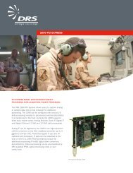
Photo courtesy of the U.S. Air Force, U.S. Navy & U.S. Army<br />
<strong>SI</strong>-<strong>9147B</strong> <strong>DUAL</strong>-<strong>CHANNEL</strong> <strong>6U</strong> <strong>VXS</strong> <strong>VHF</strong>/<strong>UHF</strong> <strong>DIGITAL</strong> <strong>TUNER</strong><br />
The DRS <strong>SI</strong>-<strong>9147B</strong> is a Dual-Channel Wideband <strong>VHF</strong>/<strong>UHF</strong><br />
Tuner that provides independent or phase-coherent<br />
conversion of RF signals from 20 MHz to 3,000 MHz. An<br />
analog IF output is centered at 76.8 MHz. The <strong>SI</strong>-<strong>9147B</strong><br />
also includes a digital back end that provides wideband<br />
16-bit analog-to-digital (A/D) converters, 12 A<strong>SI</strong>C digital<br />
downconverter channels, 12 FPGA-based digital<br />
downconverter channels, 1 GB of DDR3 memory, a user<br />
programmable field-programmable gate array (FPGA), time<br />
stamping of digital IF packets, and VRT (VITA 49) compliant<br />
data formatting. The tuner has a minimum tuning resolution<br />
of 1 MHz, but for high-speed scanning purposes,<br />
the tune resolution is in multiples of 5 MHz.<br />
The tuner features an internal Local Oscillator Distribution<br />
(LOD) assembly that allows it to accept or provide its 1st<br />
and 2nd LOs to up to eight phase coherent channels in a<br />
daisy-chain configuration without an external LOD module.<br />
Cleared by US DoD/OSR for Public Release under OSR case number 11-S-3157 dated 08.16.2011.<br />
<strong>SI</strong>-<strong>9147B</strong> Dual-Channel <strong>6U</strong> <strong>VXS</strong> <strong>VHF</strong>/<strong>UHF</strong> Digital Tuner
Architecture<br />
A functional block diagram of the tuner is shown in Figure 2. Two<br />
independent RF tuners and LOD bricks are housed in a singlewidth<br />
<strong>6U</strong> form factor. Each brick is comprised of three printed<br />
circuit cards enclosed in a single machined aluminum chassis.<br />
The dual tuner/LOD modules are mounted on the main Digital<br />
Interface and Signal Processing (DISP) board. The DISP board<br />
provides control to the tuners, the digital downconverters (DDC)<br />
and the digital signal processing resources within the FPGAs. The<br />
DISP board also controls and implements the 10 gigabit Ethernet<br />
high-speed serial protocol by which digital IF data is transferred<br />
across the P0 connector.<br />
The <strong>SI</strong>-<strong>9147B</strong> also utilizes the VITA 41.6 gigabit Ethernet control<br />
plane over the P0 connector. Front-panel connectors are available<br />
for the RF inputs, IF outputs, internal and external 10 MHz<br />
reference, LO inputs and outputs, gigabit Ethernet interface and<br />
RS 232 control.<br />
RF Tuner Module<br />
Figure 1 provides a detailed block diagram of the <strong>SI</strong>-<strong>9147B</strong> tuner<br />
assembly. RF signals are filtered at the input, either voltage-tuned<br />
tracking preselectors or sub-octave preselectors. The voltage<br />
tuned tracking preselectors can be bypassed to enable full 40<br />
MHz bandwidth below 200 MHz. Following the preselector is a<br />
low-noise RF preamplifier that provides an excellent noise figure<br />
and gain to overcome the loss of the 1st IF mixer and IF filter.<br />
Frequency coverage from 20 to 3,000 MHz is provided by<br />
converting the signal to a 1st IF of 1,750 MHz or 610 MHz,<br />
using a 1st LO that tunes from 1,750 to 3,010 MHz in 1 MHz<br />
steps. The first IF is mixed with the 2nd LO signal producing the<br />
final IF centered at 76.8 MHz. The 2nd LO is fixed at 1,673.2<br />
MHz when the 1st IF corresponds to 1,750 MHz. When the 1st IF<br />
is centered at 610 MHz, the 2nd LO is fixed at either 533.2 MHz<br />
Cleared for Public Release.<br />
Figure 2: <strong>SI</strong>-<strong>9147B</strong> Architecture<br />
or 686.8 MHz. The 76.8 MHz IF is always inverted with<br />
respect to the to the RF input. Two cascaded surface<br />
acoustic wave (SAW) filters are used to limit the bandwidth<br />
of the 76.8 MHz final IF to 40 MHz. SAW filters achieve<br />
an excellent shape factor with minimal phase and<br />
amplitude distortion.<br />
The end of the second conversion stage provides a front<br />
panel sample output for the 76.8 MHz IF and the amplification<br />
needed to interface to the A/D converter module.<br />
Fast Tuning (Turbo Mode)<br />
The tuner module has two software-selectable tuning modes.<br />
In normal tuning mode, the module has a typical tuning<br />
speed of 300 microseconds and exceptional close-in phase<br />
noise performance. In turbo tuning mode, the downconverter<br />
has a typical tuning speed of 50 microseconds with slightly<br />
degraded phase noise performance. The phase noise<br />
performance of these modes is listed in the specification table.<br />
Attenuation Control<br />
There is over 60 dB of available attenuation range in the<br />
<strong>SI</strong><strong>9147B</strong> tuner. The default attenuation implementation<br />
makes use of the values from 0 to 46 dB. This attenuation is<br />
distributed across three sections of the signal path (the 32<br />
dB front-end RF attenuator, 7 dB RF attenuator and 31 dB<br />
second IF step attenuator). The attenuation is distributed<br />
across these three attenuators based on an internal<br />
attenuation table, which is designed to maximize dynamic<br />
range versus signal level. There are several commands for<br />
each channel to allow individual channel attenuation control.<br />
The minimum step size for attenuation is 1 dB.
LO Distribution<br />
As shown in Figure 1, the LO signals can be produced within the<br />
tuner module or they can be received externally via circuits on the<br />
LO distribution board (part of the <strong>9147B</strong> module). The LO<br />
distribution circuitry allows a tuner to act as a master, a slave or<br />
an independent tuner. The master tuner drives out its 1st and 2nd<br />
LO signals for use by slave tuners, which use the input LOs for<br />
RF/IF conversions. An independent tuner, acting in a non-phase<br />
coherent mode, neither drives out nor accepts external LOs. Up<br />
to eight tuners channels can be daisy-chained for phase coherent<br />
operation. Phase coherent systems of more than eight channels<br />
can be achieved by using an external LO distribution module.<br />
ADC processing module<br />
The A/D Converter (Digitizer) module contains two 16-bit ADC<br />
devices that sample the 76.8 MHz IF at a sampling rate of 102.4<br />
MSPS. The 40 MHz IF bandwidth is digitally downconverted to an<br />
IF centered at 25.6 MHz. The ADC operates on with an internal<br />
102.4 MHz ADC master clock, or from an external clock source<br />
via its front-panel SSMC connector. This clock source is software<br />
selectable. Sampled data from the ADC module is output via<br />
low-voltage differential serial (LVDS) interface to the DISP module<br />
for processing by the FPGA circuitry.<br />
Digital Signal Processing Overview<br />
The main DISP board contains all of the hardware and firmware to<br />
provide the <strong>SI</strong>-<strong>9147B</strong> with its extensive digital signal processing<br />
(DSP) capabilities. The DSP section is based on FPGA and<br />
Application Specific Integrated Circuit (A<strong>SI</strong>C) components that<br />
offer programming flexibility.<br />
The <strong>SI</strong>-<strong>9147B</strong> DSP section consists of two independent 16-bit<br />
A/D converters, a 102.4 MHz internal A/D clock source, an<br />
FPGA for data buffering, processing, and formatting, 12<br />
A<strong>SI</strong>C-based DDC channels, 12 FPGA-based DDC channels,<br />
1-GigaByte of memory and front-panel multi-pin connectors for<br />
auxiliary control and synchronization signals. The outputs of the<br />
A/D converters are routed to a Virtex®6 FPGA located on the<br />
DISP board. The FPGA provides the ability to route the dual<br />
real-time digital IF packet streams to the memory devices for<br />
delay or any of the 24 DDC channels.<br />
The FPGA can be configured to perform a host of DSP<br />
functions including digital channelization in addition to that<br />
provided by the 24 DDCs, digital filtering, spectral analysis,<br />
or demodulation.<br />
The digital IF streams (real-time, delayed, DDC channelized, or<br />
otherwise processed digital IF packet streams ) are formatted<br />
according to the VITA 49 (VRT) data packet protocol. The VRT<br />
packets are transmitted over the <strong>SI</strong>-<strong>9147B</strong>’s P0 connector using<br />
the multi-gigabit transceiver cores embedded within the FPGA in<br />
compliance with 10 gigabit Ethernet (VITA 41.8) protocol.<br />
Cleared for Public Release.<br />
Digital Downconverters (DDCs)<br />
The <strong>SI</strong>-<strong>9147B</strong> allows programmable DDCs to be implemented<br />
both in A<strong>SI</strong>Cs and in the FPGAs. The architecture provides 12<br />
A<strong>SI</strong>C DDCs each with a decimation range from 1 to 32,768 and<br />
capable of tuning to anywhere within the digitized 40 MHz IF BW<br />
signal. These DDCs may provide output bandwidths from 1 kHz<br />
to 5 MHz. The DDCs also provide other features such as digital<br />
automatic gain control and programmable digital filtering. The<br />
FPGA also includes a special dedicated wide-band DDCs that<br />
produce 10 or 20 MHz bandwidth output.<br />
DSP Data Routing<br />
Dual wideband A/D converters digitize the full 40 MHz of analog<br />
bandwidth for both channels. These data streams are time tagged<br />
at the beginning of the process in the FPGA. The digitized data<br />
can then be routed to the FFTs, A<strong>SI</strong>C DDCs, FPGA DDCs or<br />
memory for digital signal processing purposes. Thus, any of the<br />
DDC resources can be dynamically driven by any of the A/D input<br />
signals or by a signal delayed or processed within the FPGA.<br />
Also, the same signal can be routed through two or more DDC<br />
resources to provide further signal processing and resolution.<br />
The serialized digital IF packets driven out the VITA 41 (XVS) P0<br />
connector can consist of raw digital IF data directly from the A/D<br />
Converters or of digital IF data processed or delayed by the FPGA<br />
or the A<strong>SI</strong>C DDCs or both. All data is time tagged and marked with<br />
the tuner related context fields (frequency, attenuation, etc.) in<br />
accordance with the VRT (VITA 49) standard.<br />
Streaming Digital IF<br />
The digital data output is fully compatible with industry standard<br />
hardware interface definitions identified in the VITA 41 (<strong>VXS</strong>)<br />
specification. It provides eight high-speed Serializer/Deserializer<br />
(SERDES) output streams at data rates up to 3.125 Gbps with<br />
each 8b/10b encoded digital stream providing a maximum data<br />
throughput of 2.5 Gbps for each SERDES. The <strong>SI</strong>-<strong>9147B</strong> is<br />
compliant with the 10 gigabit Ethernet (draft VITA 41.8) as well<br />
as the gigabit Ethernet control plane (VITA 41.6) extensions.<br />
Control Interface<br />
In addition to signal processing, the other major function of the<br />
DISP board is to provide control over the operations of the <strong>SI</strong>-<br />
<strong>9147B</strong> digital tuner. The DISP board supports control using its<br />
VME, gigabit Ethernet, and RS-232 interfaces. User control and<br />
status of the tuner is provided via the gigabit Ethernet (either P0<br />
or front panel). The gigabit Ethernet data transfers are handled by<br />
the PPC. User commands and queries are processed by the<br />
embedded logic within the FPGA and the appropriate control bits<br />
are sent to the programmable elements of the tuners and A<strong>SI</strong>C DDCs.<br />
In addition to gigabit Ethernet and RS-232, the front-panel<br />
connector provides hardware tune strobe signals used in the<br />
digital tuner’s frequency scan modes. In step mode, the user can<br />
predefine up to 128 tuner frequency and attenuation settings<br />
(i.e., steps) per channel to provide for the use of very<br />
sophisticated tuner scanning procedures.
SPECIFICATIONS<br />
General architecture Two 20 MHz to 3 GHz independent<br />
or coherent digital tuner channels<br />
in a single-slot <strong>6U</strong> VITA 41 (<strong>VXS</strong>)<br />
form factor<br />
Frequency range 20 to 3,000 MHz<br />
Preselector filters Voltage-tuned 30 to 459 MHz<br />
(~30% 3 dB bandwidth)<br />
Fixed sub-octave 460 to 3,000 MHz<br />
Bypass ≤ 225 MHz<br />
Tuning step size 1 MHz (normal mode, MHz<br />
frequency resolution)<br />
5 MHz (turbo mode, MHz<br />
frequency resolution)<br />
Tuning speed ≤ 300 microseconds typical for<br />
normal mode tuning<br />
≤ 1135 microseconds worst-case<br />
for normal mode tuning (Note 1)<br />
≤ 50 microseconds typical for turbo<br />
mode tuning<br />
≤ 465 microseconds worst-case<br />
for turbo mode tuning (Note 1)<br />
SSB phase noise (normal tuning mode) (Note 2)<br />
1 kHz offset -80 dBc/Hz, typical<br />
10 kHz offset -95 dBc/Hz, typical<br />
100 kHz offset -105 dBc/Hz, typical<br />
1 MHz offset -130 dBc/Hz, typical<br />
SSB phase noise (turbo tuning mode)(Note 2)<br />
1 kHz offset -80 dBc/Hz, typical<br />
10 kHz offset -90 dBc/Hz, typical<br />
100 kHz offset -95 dBc/Hz, typical<br />
1 MHz offset -120 dBc/Hz, typical<br />
INTERNAL REFERENCE<br />
Frequency 10 MHz<br />
Reference stability ±0.3 ppm (0ºC to +70ºC)<br />
Input/output connector type SSMC female<br />
Output level 0 dBm ±3 dB into 50 ohms<br />
External operation method Phase locked loop<br />
200 Hz loop bandwidth<br />
External reference frequency 10 MHz ±5 ppm<br />
External input level 0 dBm ±3 dB<br />
Cleared for Public Release.<br />
SPURIOUS PERFORMANCE<br />
In-band input third-order intercept point<br />
-5 dBm minimum (Note 3)<br />
Out-of-band input second-order intercept point<br />
+50 dBm typical<br />
+40 dBm minimum (Note 4)<br />
Image rejection TBR (30 to 1,199 MHz)<br />
70 dB (1,200 to 3,000 MHz)<br />
IF rejection 80 dB (30 to 3,000 MHz)<br />
Internally generated spurious < -100 dBm input equivalent<br />
Channel-to-channel isolation 60 dB minimum<br />
RF INPUT<br />
Connector type SMA female<br />
Impedance 50 ohms nominal<br />
VSWR at tuned frequency 2.0:1 typical<br />
3.0:1 maximum<br />
Input power without damage +20 dBm maximum<br />
Conducted LO at input -90 dBm typical<br />
-80 dBm maximum<br />
Noise figure at maximum gain 12 dB typical (30 to 3,000<br />
MHz) 14 dB maximum (30 to<br />
3,000 MHz) (Note 5)<br />
GAIN<br />
Overall gain 30 dB nominal<br />
(at A/D converter stage) (30 to 3,000 MHz)<br />
Gain variation ± 2 dB (30 to 3,000 MHz)<br />
Gain control range (default) 47 dB in 1 dB steps<br />
IF PASSBAND CHARACTERISTICS<br />
3 dB bandwidth 40 MHz nominal (two<br />
cascaded 40 MHz SAW<br />
filters), from 200 MHz to<br />
3 GHz<br />
Shape factor 1.3:1 (80:3 dB)<br />
Amplitude variation ±2 dB (30 to 3,000 MHz)<br />
Group delay variation ±90 nanoseconds typical<br />
over 90% of 3 dB bandwidth<br />
76.8 MHZ ANALOG IF OUTPUT<br />
Connector type SMA female<br />
Center frequency 76.8 MHz<br />
Impedance 50 ohms nominal<br />
Gain relative to RF input 30 dB nominal
LO OUTPUTS<br />
Output level (master mode) 0 to +10 dBm (1st LO)<br />
+4 to +12 dBm (2nd LO)<br />
Input level (slave mode) -2 dBm minimum<br />
Impedance 50 ohms nominal<br />
LO distribution connector type SSMC<br />
DSP SPECIFICATIONS<br />
A/D converter Dual LTC2208 16-bit<br />
A/D converters @ 102.4<br />
MSPS rate<br />
Dithering noise LTC2208 internal dithering<br />
enabled/disabled via software<br />
Two-tone spur-free dynamic 80 dB, typical (Note 6)<br />
range (with tuner)<br />
Single-tone spur-free dynamic 85 dB, typical (Note 6)<br />
range (with tuner)<br />
Sampling clock rate 102.4 MHz<br />
Clock input/output level +6 dBm ±3 dB into 50 ohms<br />
Time stamp Referenced to 1 PPS front panel<br />
input<br />
P0 digital IF data Rear-panel <strong>VXS</strong> P0, high-speed<br />
output protocol serial interface that is compliant<br />
with VITA 41.8;<br />
10 gigabit Ethernet<br />
Digital IF data VITA 49 – VRT compliant data<br />
packet formatting and time tag formats<br />
Digital IF output data types Real-time 102.4 MSPS<br />
ADC samples<br />
Delayed 102.4 MSPS<br />
ADC samples<br />
DDC outputs tuned to real-time<br />
or delayed ADC data (Note 7)<br />
Number of DDC channels 2 AD6636 devices provide 12<br />
independently tunable DDC<br />
channels each with a decimation<br />
range from 1 to 32,768 and with<br />
possible bandwidths from 1 kHz<br />
to 7 MHz<br />
Stored default DDC 32 defaults (bandwidths<br />
bandwidths ranging from 15 kHz to 5 MHz)<br />
Internal frequency scan 128 per channel frequency/gain<br />
steps<br />
Cleared for Public Release.<br />
FPGA dynamically Processor image can be upgraded<br />
downloadable from via 1G Ethernet (front panel or<br />
the processor via back panel)<br />
Front panel serial control Gigabit Ethernet & RS-232<br />
Weight 2.6 lbs. (1.18 kg) maximum<br />
Size Single-slot <strong>6U</strong> <strong>VXS</strong><br />
(160 x 230 mm)<br />
Power consumption<br />
Temperature<br />
TBD Watts (Note 8)<br />
Operational (convection-cooled) 0ºC to +50ºC ambient with<br />
600 CFM airflow<br />
Non-operational -40ºC to +70ºC<br />
Specification-compliant +25ºC ± 5ºC ambient with<br />
15 CFM airflow<br />
Altitude Operational at 10,000 feet<br />
(maximum ambient +20ºC)<br />
Vibration<br />
Operational Tested per DO-160D, section 8,<br />
category S2<br />
Shock<br />
Operational DO-160D, section 7, category E<br />
Notes:<br />
(1) Measured from receipt of tune command to within 1 kHz of desired frequency at<br />
76.8 MHz IF analog output. Tuning across second LO band breaks and sub MHz<br />
steps will require additional settling time.<br />
(2) Measured from RF through final IF, with 1-MHz tuning resolution only. In Turbo<br />
Tuning Mode, measured from RF through final IF, with 5 MHz tuning resolution only.<br />
Plots showing measured close-in phase noise performance data at 1 Hz to 1 kHz<br />
offsets are available upon request.<br />
(3) Measured with two tones inside the final IF bandwidth, at -7 dBFS. Attenuation set<br />
to 0 dB. Tuned frequencies of 30 to 3000 MHz. In-band intercept point<br />
specifications are referenced to the 76.8 MHz IF output only.<br />
(4) Measured with two tones outside the RF preselector passband. Attenuation set to<br />
0 dB. Tuned frequencies of 30 to 3,000 MHz. Input second-order intercept point<br />
performance will degrade when the preselector-bypass path is selected.<br />
(5) Noise figure specification assumes non-coherent (independent) tuner operation. In<br />
an N-channel daisy-chained coherent implementation, expect typical and worstcase<br />
noise figure specs to increase by a maximum of N/2 dB at the slave channel<br />
farthest from the master channel.<br />
(6) Two tones at -7 dBFS or a single-tone at -1 dBFS will not produce spurious signals<br />
greater than –80 dBFS or –85 dBFS respectively. Measured with tuner attenuation<br />
set to 0 dB, and dither enabled.<br />
(7) Initial outputs supported will include real-time and delayed ADC samples that are<br />
time stamped. Outputs from the A<strong>SI</strong>C DDC channels will also be supported. Other<br />
possible formats will follow in later revisions of this product.<br />
(8) Typical steady-state power consumption of base <strong>SI</strong>-<strong>9147B</strong> configuration at +25°C<br />
ambient in non-phase-coherent (independent) and normal tuning speed mode.<br />
Expect up to 3.0 Watt higher when in phase-coherent (Master/Slave) and turbo<br />
tuning speed mode. Requires +3.3V, +5V, and +12V VME supply voltages.
HIGHLIGHTS<br />
• Two wideband tuner channels in a single-slot <strong>6U</strong><br />
AN<strong>SI</strong>/VITA 41.0 (XVS) compliant card<br />
• 20 MHz to 3 GHz frequency range<br />
• 40 MHz instantaneous IF bandwidth (20% bandwidth<br />
below 200 MHz when voltage-tuned tracking preselectors<br />
are engaged)<br />
• 76.8 MHz analog IF output<br />
• 102.4 MHz sampling rate<br />
• 16-bit A/D converters<br />
• Data transferred via 10 gigabit Ethernet (draft VITA 41.8)<br />
over 8 high-speed SERDES channels (each @ 3.125 Gbps)<br />
on the P0 connector<br />
• Out of band Gigabit Ethernet control on P0 (VITA 41.6)<br />
• Front panel GigE I/O<br />
• VITA 49 (VRT) digital IF formatting<br />
All trademarks and registered trademarks are the property of their respective owners.<br />
DRS ICAS, LLC.<br />
21 Continental Boulevard, Merrimack, NH 03054 Tel: 603.429.0111 Fax 603.429.0155 www.drs-ds.com marketing@drs-ds.com<br />
(AS 9100, Rev. C, ISO 9001:2008, CMMI Level 3, Registered Company)<br />
Cleared for Public Release – DS FSO Dated 13 July 2011.<br />
Figure 1: RF Converter Detailed Block Diagram<br />
• Software-selectable phase-coherency of up to 8 channels<br />
without external LO Distribution module<br />
• Typical 300-microsecond tuning speed in normal mode<br />
• Typical 50-microsecond tuning speed in turbo mode<br />
• Field Upgradable with network based booting capability<br />
• Participate into system wide health and status monitoring<br />
• <strong>VXS</strong> based redundancy capable<br />
• Frequency scan modes<br />
• 1 GByte DDR3 memory on the FPGA<br />
• 256 MBytes DDR2 memory on the embedded µP<br />
• 12 A<strong>SI</strong>C digital downconverter channels<br />
- 1-32,768 decimation range<br />
- DDC bandwidths of 1 kHz to 7 MHz<br />
- Configurable filtering & gain control<br />
• User programmable FPGA for DSP functions (call factory)<br />
• Ethernet, or RS-232 control<br />
Specifications subject to change without notice. Copyright © DRS ICAS, LLC 2012. All Rights Reserved.<br />
Export of DRS ICAS, LLC products may be subject to U.S. Export Controls. U.S. Export licenses may be required.<br />
DRS MER V11 01/09/11