

MC33199, Automotive ISO 9141 Serial Link Driver - Freescale ...
MC33199, Automotive ISO 9141 Serial Link Driver - Freescale ...
MC33199, Automotive ISO 9141 Serial Link Driver - Freescale ...

You also want an ePaper? Increase the reach of your titles
YUMPU automatically turns print PDFs into web optimized ePapers that Google loves.
<strong>Freescale</strong> Semiconductor<br />
Technical Data<br />
<strong>Automotive</strong> <strong>ISO</strong> <strong>9141</strong> <strong>Serial</strong> <strong>Link</strong><br />
<strong>Driver</strong><br />
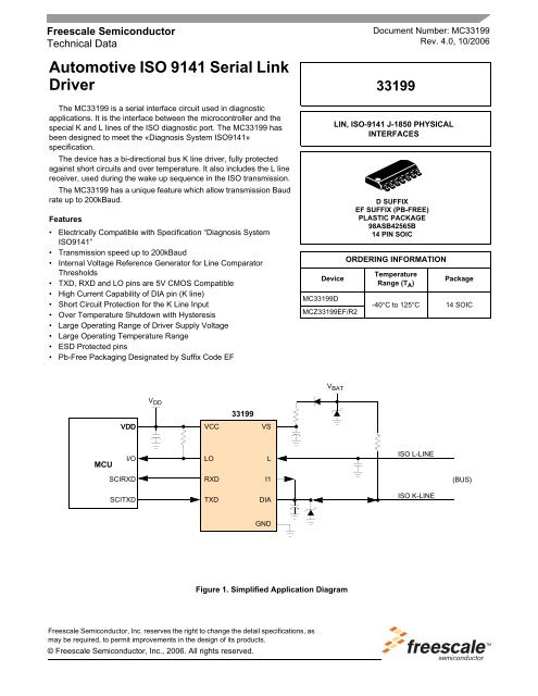
The <strong>MC33199</strong> is a serial interface circuit used in diagnostic<br />
applications. It is the interface between the microcontroller and the<br />
special K and L lines of the <strong>ISO</strong> diagnostic port. The <strong>MC33199</strong> has<br />
been designed to meet the «Diagnosis System <strong>ISO</strong><strong>9141</strong>»<br />
specification.<br />
The device has a bi-directional bus K line driver, fully protected<br />
against short circuits and over temperature. It also includes the L line<br />
receiver, used during the wake up sequence in the <strong>ISO</strong> transmission.<br />
The <strong>MC33199</strong> has a unique feature which allow transmission Baud<br />
rate up to 200kBaud.<br />
Features<br />
• Electrically Compatible with Specification “Diagnosis System<br />
<strong>ISO</strong><strong>9141</strong>”<br />
• Transmission speed up to 200kBaud<br />
• Internal Voltage Reference Generator for Line Comparator<br />
Thresholds<br />
• TXD, RXD and LO pins are 5V CMOS Compatible<br />
• High Current Capability of DIA pin (K line)<br />
• Short Circuit Protection for the K Line Input<br />
• Over Temperature Shutdown with Hysteresis<br />
• Large Operating Range of <strong>Driver</strong> Supply Voltage<br />
• Large Operating Temperature Range<br />
• ESD Protected pins<br />
• Pb-Free Packaging Designated by Suffix Code EF<br />
VDD<br />
I/O<br />
MCU<br />
SCIRXD<br />
SCITXD<br />
V DD<br />
VCC<br />
Figure 1. Simplified Application Diagram<br />
<strong>Freescale</strong> Semiconductor, Inc. reserves the right to change the detail specifications, as<br />
may be required, to permit improvements in the design of its products.<br />
© <strong>Freescale</strong> Semiconductor, Inc., 2006. All rights reserved.<br />
LO<br />
RXD<br />
TXD<br />
33199<br />
VS<br />
L<br />
I1<br />
DIA<br />
GND<br />
Device<br />
<strong>MC33199</strong>D<br />
MCZ33199EF/R2<br />
Document Number: <strong>MC33199</strong><br />
Rev. 4.0, 10/2006<br />
33199<br />
LIN, <strong>ISO</strong>-<strong>9141</strong> J-1850 PHYSICAL<br />
INTERFACES<br />
V BAT<br />
D SUFFIX<br />
EF SUFFIX (PB-FREE)<br />
PLASTIC PACKAGE<br />
98ASB42565B<br />
14 PIN SOIC<br />
ORDERING INFORMATION<br />
Temperature<br />
Range (T A )<br />
Package<br />
-40°C to 125°C 14 SOIC<br />
<strong>ISO</strong> L-LINE<br />
<strong>ISO</strong> K-LINE<br />
(BUS)
INTERNAL BLOCK DIAGRAM<br />
33199<br />
REF-OUT<br />
LO<br />
REF-IN-L<br />
REF-IN-K<br />
RXD<br />
TXD<br />
V CC<br />
<strong>Driver</strong><br />
INTERNAL BLOCK DIAGRAM<br />
C2<br />
C1<br />
+<br />
–<br />
–<br />
+<br />
VCC<br />
Reference<br />
Generator<br />
Current<br />
Limit<br />
33199<br />
Thermal<br />
Shutdown<br />
Figure 2. 33199 Simplified Internal Block Diagram<br />
Analog Integrated Circuit Device Data<br />
2 <strong>Freescale</strong> Semiconductor<br />
I1<br />
Source<br />
VS<br />
Protection<br />
L<br />
I1<br />
DIA<br />
GND
PIN CONNECTIONS<br />
VCC<br />
REF-IN-L<br />
REF-IN-K<br />
33199<br />
Figure 3. 33199 Pin Connections<br />
PIN CONNECTIONS<br />
Table 1. Pin Definitions<br />
A functional description of each pin can be found in the Functional Pin Description section, beginning on page 12.<br />
Pin Number Pin Name Definition<br />
1 VCC 5V typical power supply pin. typical supply current is less than 1.5mA<br />
2 REF-IN-L Input reference for C2 comparator.<br />
3 REF-IN-K Input reference for C1 comparator.<br />
4 LO This pin control Sleep Mode, Transmit Level, and Speed. It has a weak pulldown.<br />
5 RXD Open drain output of the data on BUS. A recessive bus = a logic [1], a dominant bus = logic [0]. An<br />
external pullup is required.<br />
6 TXD Data input here will appear on the BUS pin. A logic [0] will assert the bus, a logic [1] will make the bus<br />
go to the recessive state.<br />
7, 8 NC No internal connection to these pins.<br />
9 DIA Provides a battery-level logic signal.<br />
10 GND Electrical Common Ground and Heat removal. A good thermal path will also reduce the die<br />
temperature.<br />
11 I1 Power input. An external diode is needed for reverse battery protection.<br />
12 L The external bus load resistor connects here to prevent bus pullup in the event of loss of module<br />
ground.<br />
13 VS This pin connects to the bus through external components.<br />
14 REF-OUT Internal reference voltage generator output pin.<br />
LO<br />
RXD<br />
TXD<br />
NC<br />
1<br />
2<br />
3<br />
4<br />
5<br />
6<br />
7<br />
REF-OUT<br />
Analog Integrated Circuit Device Data<br />
<strong>Freescale</strong> Semiconductor 3<br />
14<br />
13<br />
12<br />
11<br />
10<br />
9<br />
8<br />
VS<br />
L<br />
I1<br />
GND<br />
DIA<br />
NC<br />
33199
ELECTRICAL CHARACTERISTICS<br />
MAXIMUM RATINGS<br />
33199<br />
ELECTRICAL CHARACTERISTICS<br />
MAXIMUM RATINGS<br />
Table 2. Maximum Ratings<br />
All voltages are with respect to ground unless otherwise noted. Exceeding these ratings may cause a malfunction or<br />
permanent damage to the device.<br />
ELECTRICAL RATINGS (1)<br />
VS Supply Pin<br />
DC Voltage Range<br />
Transient Pulse (2)<br />
Ratings Symbol Value Unit<br />
Analog Integrated Circuit Device Data<br />
4 <strong>Freescale</strong> Semiconductor<br />
V S<br />
V PULSE<br />
0.5 to + 40<br />
2 to + 40<br />
VCC Supply DC Voltage Range V CC 0.3 to + 6.0 V<br />
DIA and L Pins (2)<br />
DC Voltage Range<br />
- 0.5 TO + 38<br />
V<br />
Transient Pulse (clamped by internal diode)<br />
-2<br />
V<br />
DC Source Current<br />
- 50<br />
mA<br />
DIA Low Level Sink Current<br />
INT. LIMIT<br />
mA<br />
TXD DC Voltage Range -0.3 TO VCC +0.3 V<br />
REF-IN DC Voltage Range<br />
V<br />
VS < VCC<br />
-0.3 TO VCC VS > VCC<br />
-0.3 TO VS ESD Voltage Capability VESD +/-2000 V<br />
THERMAL RATINGS<br />
Storage Temperature T STG 55 to + 150 °C<br />
Operating Junction Temperature T J 40 to + 150 °C<br />
Thermal Resistance, Junction to air R TJA 180 C/W<br />
Max Power Dissipation (@ TA =105 °C) PD 250 mW<br />
Peak Package Reflow Temperature During Reflow (3) , (4) TPPRT Note 4. °C<br />
Notes<br />
1. The device is compatible with Specification: “Diagnosis System <strong>ISO</strong><strong>9141</strong>”<br />
2. See the test Circuit (Figure 26). Transient test pulse according to <strong>ISO</strong>76371 and DIN 40839, highest test levels<br />
3. Pin soldering temperature limit is for 10 seconds maximum duration. Not designed for immersion soldering. Exceeding these limits may<br />
cause malfunction or permanent damage to the device.<br />
4. <strong>Freescale</strong>’s Package Reflow capability meets Pb-free requirements for JEDEC standard J-STD-020C. For Peak Package Reflow<br />
Temperature and Moisture Sensitivity Levels (MSL),<br />
Go to www.freescale.com, search by part number [e.g. remove prefixes/suffixes and enter the core ID to view all orderable parts. (i.e.<br />
MC33xxxD enter 33xxx), and review parametrics.<br />
V
STATIC ELECTRICAL CHARACTERISTICS<br />
ELECTRICAL CHARACTERISTICS<br />
STATIC ELECTRICAL CHARACTERISTICS<br />
Table 3. Static Electrical Characteristics<br />
Characteristics noted under conditions V CC from 4.5V to 5.5V, V S from 4.5V to 20V unless otherwise note. Typical values<br />
reflect approximate mean at 25°C, nominal VCC and VS, at time of device characterization. Typical values noted reflect the<br />
approximate parameter means at T A = 25°C under nominal conditions unless otherwise noted.<br />
VCC PIN 1<br />
Characteristic Symbol Min Typ Max Unit<br />
VCC Supply Voltage Range V CC 4.5 5.5 V<br />
VCC Supply Current (6)<br />
REF-IN-L PIN 2 AND REF-IN-K PIN 3<br />
REF-IN-L & REF-IN-K Input Voltage Range:<br />
for 0
ELECTRICAL CHARACTERISTICS<br />
STATIC ELECTRICAL CHARACTERISTICS<br />
Table 3. Static Electrical Characteristics (continued)<br />
Characteristics noted under conditions V CC from 4.5V to 5.5V, V S from 4.5V to 20V unless otherwise note. Typical values<br />
reflect approximate mean at 25°C, nominal VCC and VS, at time of device characterization. Typical values noted reflect the<br />
approximate parameter means at T A = 25°C under nominal conditions unless otherwise noted.<br />
L INPUT PIN 12<br />
High Level Input Threshold Voltage<br />
(REF-IN-L connected to REF-OUT)<br />
Low Level Input Threshold Voltage<br />
(REF-IN-L connected to REF-OUT)<br />
33199<br />
Analog Integrated Circuit Device Data<br />
6 <strong>Freescale</strong> Semiconductor<br />
V IH<br />
V IL<br />
V REF MIN<br />
0.25V<br />
V REF MIN<br />
-0.2V<br />
V REF<br />
0.325V<br />
V REF<br />
-0.125V<br />
V REF MAX<br />
0.4V<br />
V REF MAX<br />
-0.05V<br />
Input Hysteresis V HYST 300 450 600 mV<br />
Leakage Current I LEAK 4.0 10 16 µΑ<br />
L1 INPUT PIN 11<br />
Static Source Current I 1S -4.0 -3.0 -2.0 mA<br />
Static Saturation Voltage @ I1S=-2mA V I1SAT V S - 1.2 V S - 0.8 V S V<br />
Dynamic Source Current I 1D -120 -80 -40 mA<br />
Dynamic Saturation Voltage @ I1S=-40mA V I1DSAT V S - 2.7 V S - 0.85 V S V<br />
VS PIN 13<br />
VS Supply Voltage Range V S 4.5 20 V<br />
VS Supply Current I S 0.5 1.3 2.0 mA<br />
REF-OUT PIN 14<br />
Output Voltage :<br />
@ 3 < VS < 5.6V & IRO = +-10µΑ<br />
@ 5.6 < V S < 18V & IRO = +-10µΑ<br />
@ 18 < V S < 40V & IRO = +-10µΑ<br />
Characteristic Symbol Min Typ Max Unit<br />
V REF<br />
2.7<br />
0.5 x V S<br />
8.5<br />
3.3<br />
0.56 x V S<br />
10.8<br />
Maximum output current I OUT -50 50 µΑ<br />
Pull-up resistor to VCC R PU 3.0 8.0 12 kΩ<br />
6. Measured with TXD=VCC, I1=VS, DIA & L high, no load, REF-IN-L and REF-IN-K connected to REF-OUT<br />
V<br />
V<br />
V
Table 4. Dynamic Electrical Characteristics<br />
DYNAMIC ELECTRICAL CHARACTERISTICS<br />
ELECTRICAL CHARACTERISTICS<br />
DYNAMIC ELECTRICAL CHARACTERISTICS<br />
Characteristics noted under conditions Vcc from 4.5V to 5.5V, Vs from 4.5V to 20V unless otherwise noted. Typical values<br />
noted reflect the approximate parameter means at T A = 25°C under nominal conditions unless otherwise noted.<br />
DELAY TIMING<br />
Characteristic Symbol Min Typ Max Unit<br />
Transmission Speed 1/T BIT 0.0 200k Baud<br />
High or Low Bit Time T BIT 5.0 µs<br />
Rxd Output :<br />
Low to High Transition Delay Time<br />
High to Low Transition Delay Time<br />
LO Output :<br />
Low to High Transition Delay Time<br />
High to Low Transition Delay Time<br />
DIA Output :<br />
Low to High Transition Delay Time<br />
High to Low Transition Delay Time<br />
I1 Output @ VS-I1 > 2.7V :<br />
Rise time<br />
Hold Time<br />
Analog Integrated Circuit Device Data<br />
<strong>Freescale</strong> Semiconductor 7<br />
t RDR<br />
t DRF<br />
t LDR<br />
t LDF<br />
t DDR<br />
t DDF<br />
t I1R<br />
t I1F 1.5<br />
450<br />
450<br />
2.0<br />
2.0<br />
650<br />
650<br />
0.3<br />
4.5<br />
ns<br />
µs<br />
ns<br />
µs<br />
33199
ELECTRICAL CHARACTERISTICS<br />
TIMING DIAGRAMS<br />
.<br />
33199<br />
Test<br />
Points<br />
Input<br />
Signal<br />
2K<br />
2x30pF<br />
+5V +12V<br />
VCC VBAT<br />
REF-OUT<br />
REF-IN-L<br />
I1<br />
REF-IN-K<br />
TxD<br />
DIA<br />
GND<br />
+5V +12V<br />
VCC VBAT<br />
REF-OUT<br />
REF-IN-L L<br />
REF-IN-K<br />
TXD DIA<br />
LO<br />
TXD Signal<br />
4mA<br />
2mA<br />
RXD<br />
120mA<br />
40mA<br />
TIMING DIAGRAMS<br />
Test<br />
Point<br />
1nF<br />
Figure 4. TXD to DIA AC Characteristic<br />
GND<br />
Figure 5. DIA to TxD and L to LO AC Characteristics<br />
t I1H<br />
t I1R<br />
t BIT<br />
Input<br />
Signal<br />
t I1F<br />
Figure 6. Current Source I1 AC Characteristics<br />
At static HIGH or LOW level TXD, the current source I1 delivers a current of 3mA (typ). Only during LOW to HIGH transition,<br />
does this current increase to a higher value in order to charge the K Line capacitor (Cl
+5V +12V<br />
VCC VBAT<br />
REF-OUT I1<br />
REF-IN-L<br />
REF-IN-K<br />
DIA<br />
TXD<br />
Figure 7. Current Source I1 and DIA Discharge current test schematic<br />
Figure 8. ICC Supply Current versus Temperature<br />
25°C<br />
Input<br />
Signal<br />
GND<br />
Figure 9. VS Supply Current versus VS Supply Voltage<br />
LO<br />
RXD<br />
ELECTRICAL PERFORMANCE CURVES<br />
-40°C<br />
125°C<br />
DIA discharge<br />
current<br />
To Oscilloscope<br />
ELECTRICAL CHARACTERISTICS<br />
ELECTRICAL PERFORMANCE CURVES<br />
Figure 10. IS Supply Voltage versus VS Supply Voltage<br />
Figure 11. VS Voltage versus IS Current<br />
(V CC=5.5V, V DIA, L, I1=20V<br />
Analog Integrated Circuit Device Data<br />
<strong>Freescale</strong> Semiconductor 9<br />
33nF<br />
10Ω<br />
I1 pulse<br />
current<br />
33199
ELECTRICAL CHARACTERISTICS<br />
ELECTRICAL PERFORMANCE CURVES<br />
Figure 12. REF-OUT Voltage versus VS Supply Voltage<br />
Figure 13. REF-OUT Voltage versus REF-OUT Current<br />
Figure 14. L and DIA Hysteresis versus Temperature<br />
33199<br />
Figure 15. L and DIA Current versus L and DIA Voltage<br />
I DIA = 40mA<br />
Figure 16. DIA Saturation Voltage versus Temperature<br />
Figure 17. DIA Current Limit versus Temperature<br />
Analog Integrated Circuit Device Data<br />
10 <strong>Freescale</strong> Semiconductor
Figure 18. RXD Pull-up Resistor versus Temperature<br />
Figure 19. TXD and LO Saturation Voltage versus<br />
Temperature<br />
I=2mA<br />
Figure 20. I1 Saturation Voltage versus Temperature<br />
LO<br />
I=40mA<br />
RXD<br />
ELECTRICAL CHARACTERISTICS<br />
ELECTRICAL PERFORMANCE CURVES<br />
Figure 21. I1 Output DC Current versus Temperature<br />
Figure 22. I1 Output Pulse Current versus VS Supply<br />
Voltage<br />
Figure 23. I1 Pulse Current Width versus Temperature<br />
Analog Integrated Circuit Device Data<br />
<strong>Freescale</strong> Semiconductor 11<br />
33199
FUNCTIONAL DESCRIPTION<br />
INTRODUCTION<br />
33199<br />
FUNCTIONAL DESCRIPTION<br />
INTRODUCTION<br />
The <strong>MC33199</strong> is a serial interface circuit used in diagnostic applications. It is the interface between the microcontroller and<br />
the special K and L lines of the <strong>ISO</strong> diagnostic port. The <strong>MC33199</strong> has been designed to meet the «Diagnosis System <strong>ISO</strong><strong>9141</strong>»<br />
specification.<br />
This product description will detail the functionality of the device (see Figure 2, 33199 Simplified Internal Block Diagram). First,<br />
the power supply and reference voltage generator will be discussed, then the paths functions between MCU, K and L lines will<br />
be detailed. A dedicated paragraph will tell about the special functionality of the I1 pin, which allow high Baud rates transmission.<br />
VCC (VCC)<br />
5V typical power supply pin. Typical supply current is less<br />
than 1.5mA.<br />
REF-IN-L (REF-IN-L)<br />
Input reference for C2 comparator. This input can be<br />
connected directly to REF-OUT, with or without a resistor<br />
network, or to an external reference.<br />
REF-IN-K (REF-IN-K)<br />
Input reference for C1 comparator. This input can be<br />
connected directly to REF-OUT, with or without a resistor<br />
network, or to an external reference.<br />
LO (LO)<br />
Output of C2 comparator, normally connected to a microcontroller<br />
I/O. If L input > (REF-IN-L + Hyst/2) then output LO<br />
is in high state. If L< (REF-IN-L - Hyst/2) then output LO is in<br />
low state, output transistor ON.<br />
This pin is an open collector structure. A Pull up resistor<br />
should be added to VCC.<br />
Drive capability of this output is 5mA.<br />
RXD (RXD)<br />
Receive output, normally connected to a microcontroller I/<br />
O.<br />
If DIA input > (REF-IN-L + Hyst/2) then output LO is in high<br />
state.<br />
If DIA < (REF-IN-L - Hyst/2) then output LO is in low state,<br />
output transistor ON. This pin has an internal pull up resistor<br />
to VCC (2Kohm typ). Drive capability of this output is 5mA<br />
TXD (TXD)<br />
Transmission input, is normally connected to a<br />
microcontroller I/O.This pin controls DIA output. If Txd is high,<br />
the output DIA transistor is OFF. If Txd is low the DIA output<br />
transistor is ON.<br />
DIA (DIA)<br />
Input / Output Diagnosis Bus line pin. This pin is an open<br />
collector structure, protected against over current and short<br />
FUNCTIONAL PIN DESCRIPTION<br />
circuit to VBAT (VS). When turning ON (TXD low), this pin will<br />
pull the Bus line to Gnd, the current into DIA will be internally<br />
limited to 60mA typ.<br />
The internal power transistor has a thermal shutdown<br />
circuit, which forces the DIA output OFF in case of over<br />
temperature.<br />
DIA is also the C1 comparator input. It is protected against<br />
both positive and negative over voltage by a 38V zener diode.<br />
This pin exhibits a constant input current of 7.5?A.<br />
GND (GND)<br />
Gnd reference for the entire device.<br />
I1 (I1)<br />
Bus source current pin. It is normally tied to DIA pin and to<br />
the Bus line.<br />
At static HIGH or LOW level Txd, the current source I1<br />
delivers a current of 3mA (typ). Only during LOW to HIGH<br />
transition, does this current increase to a higher value in<br />
order to charge the key line capacitor (Cl
POWER SUPPLIES AND REFERENCE VOLTAGE<br />
The device has two power supplies :<br />
A 5V supply, VCC, normally connected to the MCU supply<br />
voltage. This pin sinks typically 1mA during operation. A<br />
VBAT supply voltage, VS, normally tied to the car battery<br />
voltage. This pin can sustain up to 40V DC. Care should be<br />
taken for reverse battery protection and transient voltages<br />
higher than 40V.<br />
The voltage reference generator is supplied from both<br />
VCC and VBAT. It provides reference voltage for the K and L<br />
lines comparators thresholds. The reference voltage is<br />
dependant on VBAT voltage : it is linear versus VBAT<br />
voltage, for VBAT from 5.6V to 18V. Below 5.6V and over<br />
18V the reference voltage is clamped (see Figure 12). The<br />
reference is connected externally to the device, through REF-<br />
OUT pin. It is available for other needs. It can supplied 50µΑ<br />
max (see Figure 13).<br />
PATH FUNCTIONS BETWEEN MCU, K AND L<br />
LINES<br />
The path function from the MCU to the K line is composed<br />
of a driver interfacing directly with the MCU through the TXD<br />
pin. The TXD pin is CMOS compatible. This driver controls a<br />
power transistor which can be turned ON or OFF. When it is<br />
ON, it pull the DIA pin low. This pin is known as K line in the<br />
<strong>ISO</strong> <strong>9141</strong> specification. The DIA pin structure is open<br />
collector, without pull up component. This allow the<br />
connection of several <strong>MC33199</strong> on the K line and the use of<br />
a single pull up resistor per system (see Figure 25). In order<br />
to protect the DIA pin against short circuits to VBAT, the<br />
device incorporates a current limitation (see Figure 17) and a<br />
thermal shutdown. This current limitation will also act when<br />
the device drives a K line bus exhibiting large parasitic<br />
capacitor value (see Special functionality of I1 pin).<br />
The path from this DIA pin, or K line, to the MCU is done<br />
through a comparator. The comparator threshold voltage is<br />
connected to REF-IN-K pin. It can be tied to the REF-OUT<br />
voltage, if the VBAT dependant threshold is to be achieved.<br />
The second input of this comparator is internally connected<br />
to DIA pin. The output of the comparator is available on RXD<br />
output pin, normally connected to a MCU I/O port. RXD pin<br />
has a 2kOhms internal pull up resistor.<br />
The path from the L line, used during wake-up sequence<br />
of the transmission, to the MCU is done through a second<br />
comparator. The comparator threshold voltage is connected<br />
to REF-IN-L pin. As the REF-IN-K pin, it can be tied to the<br />
REFOUT voltage, if the VBAT dependant threshold need to<br />
be achieved. The second input of this comparator is internally<br />
FUNCTIONAL DEVICE OPERATION<br />
FUNCTIONAL DEVICE OPERATION<br />
connected to L pin. The output of the comparator is available<br />
on LO output pin, which is an open collector structure. LO is<br />
normally connected to a MCU I/O port.<br />
The DIA, and L pins can sustain up to 38V DC. Care<br />
should be taken for reverse battery protection and transient<br />
voltages higher than 38V.<br />
The DIA and L pins both have internal pull down current<br />
source of typically 7.5µΑ (see Figure 15). So the L line<br />
exhibits a 10µΑ pull down current. The DIA pin has the same<br />
behavior when it is in OFF state, that is when TXD is at logic<br />
high level.<br />
SPECIAL FUNCTIONALITY OF I1 PIN<br />
The <strong>MC33199</strong> has a unique feature which allows the<br />
transmission Baud rate to be up to 200kBaud. In practice, the<br />
K line can be several meters long, and thus can have a large<br />
parasitic capacitor value. This parasitic capacitor value will<br />
slow down the low to high transition of the K line, and indeed<br />
will limit the Baud rate transmission. For the K line to go from<br />
low to high level, the parasitic capacitor need to be charged,<br />
and it can only be charged by the pull up resistor. A low pull<br />
up resistor value would result in fast charge time of the<br />
capacitor, but also in large output current, and large power<br />
dissipation in the driver.<br />
To avoid this problem, the <strong>MC33199</strong> incorporates a<br />
dynamic current source, which is temporary activated at the<br />
low to high transition of the TXD pin, that is when the DIA pin<br />
or K line should switch from low to high level (see Figure 6 &<br />
Figure 7).<br />
This current source is available at I1 pin. It has a typical<br />
value of 80mA. It is activated for 4µs (see Figure 22 &<br />
Figure 23) and is automatically disabled after this time.<br />
During that time it will charge the K line parasitic capacitor.<br />
This extra current will quickly rise the K line voltage up to the<br />
Vbat, and will result in reduce rise time on the K line. With this<br />
feature the <strong>MC33199</strong> can ensure Baud rate transmission of<br />
up to 200kBaud.<br />
During high to low transition on the K line, the parasitic<br />
capacitor of the bus line will be discharged by the output<br />
transistor of the DIA pin. In this case, the total current may<br />
exceed the internal current limitation of the DIA pin. If so, the<br />
current limitation will act, and discharge current will be limited<br />
to typically 60mA (See Figure 7 & Figure 17).<br />
If a high Baud rate is necessary, the I1 pin need to be<br />
connected to the DIA as shown in the typical application<br />
Figure 24. The I1 pin can also be left open, if the I1<br />
functionality and high Baud rate are not suited in the<br />
application.<br />
Analog Integrated Circuit Device Data<br />
<strong>Freescale</strong> Semiconductor 13<br />
33199
TYPICAL APPLICATIONS<br />
33199<br />
MCU<br />
REF-OUT<br />
LO<br />
REF-IN-L<br />
REF-IN-K<br />
RXD<br />
TXD<br />
Reference<br />
Generator<br />
+<br />
C2<br />
-<br />
Vcc<br />
-<br />
C1<br />
+<br />
<strong>Driver</strong><br />
TYPICAL APPLICATIONS<br />
VCC : 5V<br />
Thermal<br />
Shutdown<br />
Current<br />
Limit<br />
VS<br />
Protection<br />
I1<br />
source<br />
CAR ELECTRONIC CONTROL UNIT<br />
Figure 24. Logic Diagram and Application Schematic<br />
Analog Integrated Circuit Device Data<br />
14 <strong>Freescale</strong> Semiconductor<br />
L<br />
I1<br />
DIA<br />
GND<br />
+VBAT<br />
L Line<br />
K Line<br />
R PU<br />
SERVICE TESTER<br />
or<br />
End of Line<br />
manufacturer<br />
programmation or<br />
checking system<br />
TxD<br />
RxD
MCU <strong>MC33199</strong><br />
MCU<br />
E.C.U # 1<br />
E.C.U # 2<br />
CAR<br />
<strong>MC33199</strong><br />
+12V<br />
Figure 25. Typical Application with Several ECUs<br />
VBAT<br />
I1<br />
DIA<br />
GND<br />
100nF<br />
L<br />
Other ECUs<br />
D2<br />
Figure 26. Test Circuit for Transient Schaffner Pulses<br />
TYPICAL APPLICATIONS<br />
Test pulses are directly applied to VS and via a capacitor of 1nF to DIA and L. The voltage VS is limited to -2V/38V by the<br />
transient suppressor diode D1. Pulses can occor simultaneously or separately.<br />
Analog Integrated Circuit Device Data<br />
<strong>Freescale</strong> Semiconductor 15<br />
+Vbat<br />
R PU<br />
L Line<br />
K Line<br />
CAR <strong>ISO</strong> DIAGNOSTIC CONNECTOR<br />
SERVICE TESTER<br />
or<br />
End of Line<br />
manufacturer<br />
programmation or<br />
checking system<br />
Fig 6 : Typical application with several ECUs<br />
D1<br />
2x330pF<br />
2x1nF<br />
Schaffner<br />
Generator<br />
33199
PACKAGING<br />
PACKAGE DIMENSIONS<br />
33199<br />
PACKAGING<br />
PACKAGE DIMENSIONS<br />
For the most current package revision, visit www.freescale.com and perform a keyword search using the “98A” listed below.<br />
D SUFFIX<br />
EF-SUFFIX (PB-FREE)<br />
PLASTIC PACKAGE<br />
98ASB42565B<br />
ISSUE H<br />
Analog Integrated Circuit Device Data<br />
16 <strong>Freescale</strong> Semiconductor
Revision Date Description of Changes<br />
REVISION HISTORY<br />
REVISION HISTORY<br />
2.0 8/2006 • Implemented Revision History page<br />
• Added EF Pb-FREE suffix<br />
• Revised Figure 1, Simplified Application Drawing.<br />
• Converted to <strong>Freescale</strong> format and updated to the prevailing form and style<br />
• Removed <strong>MC33199</strong>EF/R2 and replaced with MCZ33199EF/R2 in the Ordering Information block<br />
3.0 9/2006 • Made unit label corrections on Transmission Speed, High or Low Bit Time, LO Output :, and I1<br />
Output @ VS-I1 > 2.7V : on page 7.<br />
4.0 10/2006 • Removed Peak Package Reflow Temperature During Reflow (solder reflow) parameter from<br />
Maximum Ratings on page 4. Added note with instructions to obtain this information from<br />
www.freescale.com.<br />
Analog Integrated Circuit Device Data<br />
<strong>Freescale</strong> Semiconductor 17<br />
33199
How to Reach Us:<br />
Home Page:<br />
www.freescale.com<br />
E-mail:<br />
support@freescale.com<br />
USA/Europe or Locations Not Listed:<br />
<strong>Freescale</strong> Semiconductor<br />
Technical Information Center, CH370<br />
1300 N. Alma School Road<br />
Chandler, Arizona 85224<br />
+1-800-521-6274 or +1-480-768-2130<br />
support@freescale.com<br />
Europe, Middle East, and Africa:<br />
<strong>Freescale</strong> Halbleiter Deutschland GmbH<br />
Technical Information Center<br />
Schatzbogen 7<br />
81829 Muenchen, Germany<br />
+44 1296 380 456 (English)<br />
+46 8 52200080 (English)<br />
+49 89 92103 559 (German)<br />
+33 1 69 35 48 48 (French)<br />
support@freescale.com<br />
Japan:<br />
<strong>Freescale</strong> Semiconductor Japan Ltd.<br />
Headquarters<br />
ARCO Tower 15F<br />
1-8-1, Shimo-Meguro, Meguro-ku,<br />
Tokyo 153-0064<br />
Japan<br />
0120 191014 or +81 3 5437 9125<br />
support.japan@freescale.com<br />
Asia/Pacific:<br />
<strong>Freescale</strong> Semiconductor Hong Kong Ltd.<br />
Technical Information Center<br />
2 Dai King Street<br />
Tai Po Industrial Estate<br />
Tai Po, N.T., Hong Kong<br />
+800 2666 8080<br />
support.asia@freescale.com<br />
For Literature Requests Only:<br />
<strong>Freescale</strong> Semiconductor Literature Distribution Center<br />
P.O. Box 5405<br />
Denver, Colorado 80217<br />
1-800-441-2447 or 303-675-2140<br />
Fax: 303-675-2150<br />
LDCFor<strong>Freescale</strong>Semiconductor@hibbertgroup.com<br />
<strong>MC33199</strong><br />
Rev. 4.0<br />
10/2006<br />
RoHS-compliant and/or Pb-free versions of <strong>Freescale</strong> products have the functionality<br />
and electrical characteristics of their non-RoHS-compliant and/or non-Pb-free<br />
counterparts. For further information, see http://www.freescale.com or contact your<br />
<strong>Freescale</strong> sales representative.<br />
For information on <strong>Freescale</strong>’s Environmental Products program, go to http://<br />
www.freescale.com/epp.<br />
Information in this document is provided solely to enable system and software<br />
implementers to use <strong>Freescale</strong> Semiconductor products. There are no express or<br />
implied copyright licenses granted hereunder to design or fabricate any integrated<br />
circuits or integrated circuits based on the information in this document.<br />
<strong>Freescale</strong> Semiconductor reserves the right to make changes without further notice to<br />
any products herein. <strong>Freescale</strong> Semiconductor makes no warranty, representation or<br />
guarantee regarding the suitability of its products for any particular purpose, nor does<br />
<strong>Freescale</strong> Semiconductor assume any liability arising out of the application or use of any<br />
product or circuit, and specifically disclaims any and all liability, including without<br />
limitation consequential or incidental damages. “Typical” parameters that may be<br />
provided in <strong>Freescale</strong> Semiconductor data sheets and/or specifications can and do vary<br />
in different applications and actual performance may vary over time. All operating<br />
parameters, including “Typicals”, must be validated for each customer application by<br />
customer’s technical experts. <strong>Freescale</strong> Semiconductor does not convey any license<br />
under its patent rights nor the rights of others. <strong>Freescale</strong> Semiconductor products are<br />
not designed, intended, or authorized for use as components in systems intended for<br />
surgical implant into the body, or other applications intended to support or sustain life,<br />
or for any other application in which the failure of the <strong>Freescale</strong> Semiconductor product<br />
could create a situation where personal injury or death may occur. Should Buyer<br />
purchase or use <strong>Freescale</strong> Semiconductor products for any such unintended or<br />
unauthorized application, Buyer shall indemnify and hold <strong>Freescale</strong> Semiconductor and<br />
its officers, employees, subsidiaries, affiliates, and distributors harmless against all<br />
claims, costs, damages, and expenses, and reasonable attorney fees arising out of,<br />
directly or indirectly, any claim of personal injury or death associated with such<br />
unintended or unauthorized use, even if such claim alleges that <strong>Freescale</strong><br />
Semiconductor was negligent regarding the design or manufacture of the part.<br />
<strong>Freescale</strong> and the <strong>Freescale</strong> logo are trademarks of <strong>Freescale</strong> Semiconductor, Inc.<br />
All other product or service names are the property of their respective owners.<br />
© <strong>Freescale</strong> Semiconductor, Inc., 2006. All rights reserved.


