

Implementing Auto-Zero Calibration Technique for Accelerometers
Implementing Auto-Zero Calibration Technique for Accelerometers
Implementing Auto-Zero Calibration Technique for Accelerometers

Create successful ePaper yourself
Turn your PDF publications into a flip-book with our unique Google optimized e-Paper software.
Freescale Semiconductor<br />
Application Note<br />
<strong>Implementing</strong> <strong>Auto</strong>-<strong>Zero</strong> <strong>Calibration</strong><br />
<strong>Technique</strong> <strong>for</strong> <strong>Accelerometers</strong><br />
by: Kimberly Tuck<br />
Accelerometer Systems and Applications Engineering<br />
Tempe, AZ<br />
INTRODUCTION<br />
This application note describes why it is important to<br />
implement an auto-zero calibration function into the<br />
MMA73x0L series accelerometers and how to implement it<br />
with a microcontroller containing an analog-to-digital<br />
converter. This auto-zero compensation technique is based<br />
on sampling the accelerometer voltage output value at 0g<br />
which is the zero reference. This reference value is known as<br />
the offset voltage. The expected offset values <strong>for</strong> the<br />
MMA73x0L series accelerometers is listed in Table 1 <strong>for</strong> 0g,<br />
+1g.<br />
Table 1. Offset Values <strong>for</strong> MMA73x0L<br />
<strong>for</strong> X, Y and Z Directions<br />
© Freescale Semiconductor, Inc., 2007. All rights reserved.<br />
AN3447<br />
Rev 0, 03/2007<br />
OFFSET ERRORS AND WHY AUTO ZERO<br />
CALIBRATION IS IMPORTANT<br />
Sources of offset errors can occur device to device based<br />
on offset variations from trim errors, mechanical stresses from<br />
the package and mounting, shifts due to temperature and due<br />
to aging. These variables can all change the offset. This can<br />
be very significant <strong>for</strong> many applications. The offset error<br />
alone can affect a tilt reading on a flat surface by as much as<br />
12 degrees. That is an unacceptable error <strong>for</strong> this application.<br />
Per<strong>for</strong>ming an auto-zero calibration technique using a<br />
microcontroller with an A/D converter can reduce these errors,<br />
but note that the error correction will be limited by the<br />
resolution of the A/D converter.<br />
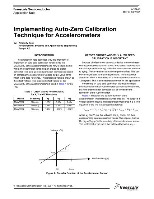
Figure 1 illustrates the transfer function of the<br />
accelerometer. This relation assumes linearity. The output is a<br />
voltage and the input is the acceleration measured in g’s. The<br />
equation of the line is expressed as follows:<br />
Device Sensitivity 0g -1g +1g<br />
MMA7360L 800mV/g 1.65V 0.85V 2.45V<br />
MMA7340L 440mV/g 1.65V 1.21V 2.09V<br />
MMA7330L 308mV/g 1.40V 1.092V 1.708V VOUT = [ ( V2 – V1) ⁄ ( g2 – g1) ]∗g+ VOFF = S∗g+ VOFF ;<br />
Voltage (V)<br />
VOFF<br />
0g<br />
S<br />
gMAX<br />
Figure 1. Transfer Function of the Accelerometer Sensor<br />
where V 2 and V 1 are two voltages and g 2 and g 1 are their<br />
corresponding input acceleration values. The slope of the line<br />
S = (V 2 -V 1 )/(g 2 -g 1 ) is the sensitivity of the accelerometer sensor.<br />
The y-intercept of the line is the voltage offset value V OFF .<br />
Acceleration (g’s)
A two point acceleration calibration can be per<strong>for</strong>med to<br />
accurately determine the sensitivity and get rid of the offset<br />
calibration errors. This can be very expensive in high volume<br />
production due to extra time involved. There<strong>for</strong>e, the<br />
sensitivity and offset data is given in the data sheet and a<br />
linear equation is used to determine the acceleration.<br />
AN3447<br />
Acceleration( g)<br />
= ( VOUT – VOFF) ⁄ S<br />
VOFF @ 0g<br />
Voltage (V)<br />
VOFF + ∆V<br />
OFFSET CALIBRATION ERRORS<br />
The minimum expected and maximum offset values at 0g<br />
<strong>for</strong> the MMA73x0L devices are listed in Table 2.<br />
Even though the offset is laser trimmed, offset can shift due<br />
to packaging stresses, aging and external mechanical<br />
stresses due to mounting and orientation. This results in offset<br />
calibration error. Table 2 lists the minimum, maximum and<br />
expected offset ranges.<br />
TEMPERATURE COEFFICIENT OF OFFSET<br />
ERRORS<br />
The offset error due to temperature is due to the<br />
Temperature Coefficient of Offset (TCO). This parameter is<br />
the rate of change of the offset when the sensor is subject to<br />
temperature. It is defined as: TCO = (∆V OFF/∆T) assuming it<br />
is linear. The MMA7360 has a TCO normalized with the span<br />
at 25ºC of ±0.03% / ºC.<br />
∆V<br />
Table 2. Offset Value Range <strong>for</strong> the MMA73XOL<br />
Accelerometer Series<br />
Device<br />
Name<br />
0g<br />
g-Range Min. Offset Expected<br />
Offset<br />
Figure 2. Effects of Offset Errors<br />
Max. Offset<br />
MMA7360L 1.5/6 1.485V 1.65V 1.815V<br />
MMA7340L 3/12 1.485V 1.65V 1.815V<br />
MMA7330L 4/16 1.316V 1.4V 1.484V<br />
If an offset error is introduced due to device-to-device<br />
variation, mechanical stresses or offset shift due to<br />
temperature, those errors will show up as an error in the<br />
acceleration reading. As shown in Figure 2, if an offset error is<br />
introduced (∆V OFF ) then there will be a corresponding error in<br />
the acceleration reading, ∆g.<br />
g g + ∆g<br />
g + ∆g = [ VOUT – ( VOFF + ∆VOFF) ] ⁄ S<br />
TECHNIQUES FOR CALIBRATING THE OFFSET<br />
VOLTAGE<br />
Manual 0g X, Y, Z Full Range <strong>Calibration</strong><br />
In order to find the 0g voltage output value of the<br />
accelerometer it is necessary to know that the device is sitting<br />
completely level. Although placing the device on the table may<br />
seem flat, this doesn’t guarantee that the device is not<br />
experiencing a slight g <strong>for</strong>ce. The device may be experiencing<br />
more that 0g due to packaging or device shifts. One method<br />
used to get an accurate and reliable 0g reading is to rotate the<br />
device from +1g through -1g. The max value will be +1g and<br />
the minimum value will be -1g. Assuming that the sensitivity is<br />
symmetric from zero to positive and from zero to negative the<br />
sensitivity of the device can be calculated by dividing by 2.<br />
Knowing the sensitivity the 0g offset value can be calculated<br />
by adding the sensitivity to the minimum value or by<br />
subtracting the sensitivity from the max value. It is also a good<br />
idea to place the part level and check the 0g offset value. It<br />
should be very close. This method must be followed <strong>for</strong> all<br />
three axes. The drawback of this technique is that it is tedious.<br />
Simple 0g X, Y, Z calibration<br />
Another method would be to assume 0g on a level surface.<br />
The device would need to be turned 90 degrees once to go<br />
from 0g XY to 0g in Z. The 0g values would be recorded this<br />
way. This technique does not guarantee as much accuracy as<br />
the previous method.<br />
Sensors<br />
2 Freescale Semiconductor<br />
∆g<br />
Acceleration (g)
Freefall <strong>Calibration</strong><br />
Another method to calibrate the device <strong>for</strong> 0g offset would<br />
be to record the offset of X, Y and Z while the device is in<br />
freefall. The possible downfall of this approach is the fact that<br />
the device may rotate while falling and put a <strong>for</strong>ce on the<br />
device. Also it may be inconvenient to recalibrate each time by<br />
putting the device in freefall. The benefit of this approach is<br />
that all three axes can be at 0g all at the same time.<br />
Simple 0g X, 0g Y, +1g Z calibration<br />
Another method that is extremely convenient would be to<br />
place the device on a flat surface so that X is at 0g, Y is at 0g<br />
and Z is at +1g. The values are recorded. The X and Y offset<br />
values would be fairly accurate, but the +1g value would have<br />
errors because this value would not be recorded at 0g. The<br />
known sensitivity would be subtracted from the +1g to<br />
calculate an assumed 0g offset value <strong>for</strong> Z. This is convenient<br />
in that the device would never need to be rotated or moved.<br />
The disadvantage of this approach is that it is the least<br />
accurate way to calibrate 0g offset of the above mentioned<br />
techniques.<br />
IMPLEMENTATION OF AUTO-ZERO WITH A<br />
MICROCONTROLLER<br />
When implementing auto-zero (a zero reference) 0g must<br />
be used. An auto-zero command can be automated by the<br />
system or it can be commanded manually. This may be<br />
somewhat dependant on the application. Note that if the auto-<br />
zero is to be per<strong>for</strong>med only once and the offset correction<br />
data is stored in memory the TCO offset error and calibration<br />
error will not be corrected if the sensor later experiences a<br />
Measure Again<br />
Start<br />
wide temperature range or later experiences an offset shift. It<br />
would be wise to per<strong>for</strong>m an auto-zero calibration at the<br />
operating temperature to compensate <strong>for</strong> the TCO and auto<br />
calibrate as often as possible to dynamically compensate <strong>for</strong><br />
system offset errors.<br />
<strong>Auto</strong>-zero can be implemented easily when the integrated<br />
sensor is interfaced to a microcontroller. The auto-zero<br />
algorithm is listed below:<br />
1. Sample the sensor output when a known zero<br />
reference is applied to the sensor (0g is the reference).<br />
Store the current 0g or +1g offset (depending on the<br />
technique used) as CZOFF .<br />
2. Sample the sensor output at the current applied<br />
acceleration. Call this CA.<br />
3. Subtract the stored offset correction, CZOFF, from CA.<br />
The acceleration being measured at the current reading<br />
is simply:<br />
For the Simple 0g X, 0g Y, +1g Z calibration technique a<br />
slightly different calculation is required <strong>for</strong> the Z axis which has<br />
recorded the CZ OFF value at +1g. The sensitivity ‘S’ must<br />
there<strong>for</strong>e be subtracted from CZ OFF in the calculation.<br />
For the Z Case:<br />
Sample Current <strong>Zero</strong> Offset, CZOFF<br />
Sample Current Acceleration, CA<br />
Calculate Acceleration<br />
AMEAS= CA-CZOFF<br />
S<br />
End<br />
Figure 3. Flow Chart of the <strong>Auto</strong>-<strong>Zero</strong> Algorithm<br />
AMEAS = [ CA – CZOFF] ⁄ S<br />
AMEAS = [ CA – ( CZOFF – S)<br />
] ⁄ S<br />
Note that the equation is simply a straight line equation<br />
where S is the sensitivity of the accelerometer. The auto-zero<br />
algorithm is shown graphically in Figure 3.<br />
<strong>Auto</strong>-<strong>Zero</strong> Command<br />
Received<br />
AN3447<br />
Sensors<br />
Freescale Semiconductor 3
Sample Code <strong>for</strong>: Simple 0g X, 0g Y, +1g Z calibration<br />
method<br />
S = Sensitivity;<br />
X0g_current = XCZOFF; Y0g_current = YCZOFF; Z1g_current = ZCZOFF; AN3447<br />
XCA = XCA_val;<br />
YCA = YCA_val;<br />
ZCA = ZCA_val;<br />
AmeasX = (XCA-X0gcurrent)/S;<br />
AmeasY = (YCA-Y0gcurrent)/S;<br />
AmeasZ = (ZCA-(Z1g_current-S))/S;<br />
Sample Code <strong>for</strong>: all other 0g calibration methods<br />
S = Sensitivity;<br />
X0g_current = XCZOFF; Y0g_current = YCZOFF; Z0g_current = ZCZOFF; XCA = XCA_val;<br />
YCA = YCA_val;<br />
ZCA = ZCA_val;<br />
AmeasX = (XCA-X0gcurrent)/S;<br />
AmeasY = (YCA-Y0gcurrent)/S;<br />
AmeasZ = (ZCA-Z0g_current)/S;<br />
A/D RESOLUTION ERROR<br />
The auto-zero calibration technique can reduce the offset<br />
errors, but the A/D converter used in this process has a limited<br />
resolution and there<strong>for</strong>e introduces an error of its own.<br />
Typically an 8 bit A/D converter is used, which cuts the 3.3V<br />
supply voltage on the MMA7360L into 255 steps, 12.9mV <strong>for</strong><br />
each step. If a 10 bit A/D converter is used this would cut the<br />
3.3V supply voltage into 1023 steps, 3.2mV <strong>for</strong> each step. A<br />
12 bit A/D converter cuts the 3.3V supply voltage by 4095<br />
steps, 0.8mV per step. There<strong>for</strong>e the resolution is much better<br />
when a larger A/D converter is used, which reduces the error.<br />
Using an 8 bit A/D converter the voltage offset would be<br />
V OFF + 0.129V = 1.779V. The V OFF can be auto-zeroed, but<br />
the A/D converter resolution remains erroneous.<br />
CONCLUSION<br />
An auto-zero calibration technique is very important <strong>for</strong><br />
minimizing offset errors. It is easily implemented into the<br />
accelerometer sensor system using a microcontroller with an<br />
A/D converter and a few lines of code. The resulting<br />
minimized offset errors of the system is limited only by the<br />
resolution of the A/D converter.<br />
REFERENCES<br />
1. AN1636, <strong>Implementing</strong> <strong>Auto</strong> <strong>Zero</strong> <strong>for</strong> Integrated<br />
Pressure Sensors, Ador Reodique, Freescale<br />
Semiconductor, Inc., Freescale Application Note.<br />
Sensors<br />
4 Freescale Semiconductor
How to Reach Us:<br />
Home Page:<br />
www.freescale.com<br />
Web Support:<br />
http://www.freescale.com/support<br />
USA/Europe or Locations Not Listed:<br />
Freescale Semiconductor, Inc.<br />
Technical In<strong>for</strong>mation Center, EL516<br />
2100 East Elliot Road<br />
Tempe, Arizona 85284<br />
+1-800-521-6274 or +1-480-768-2130<br />
www.freescale.com/support<br />
Europe, Middle East, and Africa:<br />
Freescale Halbleiter Deutschland GmbH<br />
Technical In<strong>for</strong>mation Center<br />
Schatzbogen 7<br />
81829 Muenchen, Germany<br />
+44 1296 380 456 (English)<br />
+46 8 52200080 (English)<br />
+49 89 92103 559 (German)<br />
+33 1 69 35 48 48 (French)<br />
www.freescale.com/support<br />
Japan:<br />
Freescale Semiconductor Japan Ltd.<br />
Headquarters<br />
ARCO Tower 15F<br />
1-8-1, Shimo-Meguro, Meguro-ku,<br />
Tokyo 153-0064<br />
Japan<br />
0120 191014 or +81 3 5437 9125<br />
support.japan@freescale.com<br />
Asia/Pacific:<br />
Freescale Semiconductor Hong Kong Ltd.<br />
Technical In<strong>for</strong>mation Center<br />
2 Dai King Street<br />
Tai Po Industrial Estate<br />
Tai Po, N.T., Hong Kong<br />
+800 2666 8080<br />
support.asia@freescale.com<br />
For Literature Requests Only:<br />
Freescale Semiconductor Literature Distribution Center<br />
P.O. Box 5405<br />
Denver, Colorado 80217<br />
1-800-441-2447 or 303-675-2140<br />
Fax: 303-675-2150<br />
LDCForFreescaleSemiconductor@hibbertgroup.com<br />
AN3447<br />
Rev. 0<br />
03/2007<br />
In<strong>for</strong>mation in this document is provided solely to enable system and software<br />
implementers to use Freescale Semiconductor products. There are no express or<br />
implied copyright licenses granted hereunder to design or fabricate any integrated<br />
circuits or integrated circuits based on the in<strong>for</strong>mation in this document.<br />
Freescale Semiconductor reserves the right to make changes without further notice to<br />
any products herein. Freescale Semiconductor makes no warranty, representation or<br />
guarantee regarding the suitability of its products <strong>for</strong> any particular purpose, nor does<br />
Freescale Semiconductor assume any liability arising out of the application or use of any<br />
product or circuit, and specifically disclaims any and all liability, including without<br />
limitation consequential or incidental damages. “Typical” parameters that may be<br />
provided in Freescale Semiconductor data sheets and/or specifications can and do vary<br />
in different applications and actual per<strong>for</strong>mance may vary over time. All operating<br />
parameters, including “Typicals”, must be validated <strong>for</strong> each customer application by<br />
customer’s technical experts. Freescale Semiconductor does not convey any license<br />
under its patent rights nor the rights of others. Freescale Semiconductor products are<br />
not designed, intended, or authorized <strong>for</strong> use as components in systems intended <strong>for</strong><br />
surgical implant into the body, or other applications intended to support or sustain life,<br />
or <strong>for</strong> any other application in which the failure of the Freescale Semiconductor product<br />
could create a situation where personal injury or death may occur. Should Buyer<br />
purchase or use Freescale Semiconductor products <strong>for</strong> any such unintended or<br />
unauthorized application, Buyer shall indemnify and hold Freescale Semiconductor and<br />
its officers, employees, subsidiaries, affiliates, and distributors harmless against all<br />
claims, costs, damages, and expenses, and reasonable attorney fees arising out of,<br />
directly or indirectly, any claim of personal injury or death associated with such<br />
unintended or unauthorized use, even if such claim alleges that Freescale<br />
Semiconductor was negligent regarding the design or manufacture of the part.<br />
Freescale and the Freescale logo are trademarks of Freescale Semiconductor, Inc.<br />
All other product or service names are the property of their respective owners.<br />
© Freescale Semiconductor, Inc. 2007. All rights reserved.


