display area
display area
display area

You also want an ePaper? Increase the reach of your titles
YUMPU automatically turns print PDFs into web optimized ePapers that Google loves.
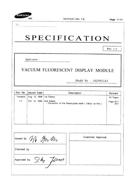
1.SCOPE<br />
SDI 16LF01UA3 (Rev 1.0)<br />
Page 2 / 11<br />
This specification applies to VFD module(Model No:16LF01UA3) manufactured by Samsung SDI.<br />
2.FEATURES<br />
2.1 Simple connection to the host system data bus via two-wired serial interface.<br />
2.2 Since a DC/DC converter is used, only +5Vdc power source is required to operate the module.<br />
2.3 One chip controller offers integral 64 x 16 bit programmable logic array, low power consumption<br />
and high reliability in services.<br />
2.4 32 brightness levels can be selected by brightness control command.<br />
2.5 High quality blue-green(505 nm) vacuum fluorescent <strong>display</strong> provides an attractive and readable<br />
medium. Other colors can be achieved by simple wavelength filters.<br />
2.6 Characters are provided in an attractive 16-segment starburst format.<br />
3.GENERAL DESCRIPTIONS<br />
3.1 This specification becomes effective after being approved by the purchaser.<br />
3.2 When any conflict is found in the specification, appropriate action shall be taken upon agreement<br />
of both parties.<br />
3.3 The expected necessary service parts should be arranged by the customer before the completion<br />
of production.<br />
4.PRODUCT SPECIFICATIONS<br />
4.1 Type<br />
Outer Dimensions<br />
Type 16LF01UA3<br />
Digit Format 16 Seg. & Comma, Decimal Point<br />
4.2 Outer Dimensions, Weight (See Fig-4 for details)<br />
Parameter Specification Unit<br />
Width<br />
Height<br />
Thickness<br />
218.0 +/-1.0<br />
45.0 +/-1.0<br />
26.5 Max<br />
Weight Typical 130 g<br />
mm<br />
mm<br />
mm<br />
Table_1<br />
Table_2
SDI 16LF01UA3 (Rev 1.0)<br />
Page 3 / 11<br />
4.3 Specifications of Display Panel (See Fig-5 for details) Table_3<br />
Parameter Symbol Specification Unit<br />
Display Size (W x H) - 173.6 x 14.25 mm<br />
Number of Digit - 16 Digits -<br />
Character Size (W x H) - 7.0 x 12.50 mm<br />
Character Pitch Cp(x) 11.0 mm<br />
Display Color - Blue-Green (Peak 505nm) mm<br />
4.4 Environment Conditions Table_4<br />
Parameter Symbol Min. Max. Unit<br />
Operating Temperature £ opr -20 +70<br />
Storage Temperature £ stg -40 +85<br />
Humidity (Operating) £¨opr 0 85 %<br />
Humidity (Non-operating) £¨stg 0 90 %<br />
Vibration (10 ~ 55 Hz) - - 4 G<br />
Shock - - 40 G<br />
4.5 Absolute Maximum Ratings Table_5<br />
Parameter Symbol Min. Max. Unit<br />
Supply Voltage VCC - 7.0 VDC<br />
Input Signal Voltage VIS -0.4 5.5 VDC<br />
4.6 Recommend Operating Conditions Table_6<br />
Parameter Symbol Min. Typ. Max. Unit<br />
Supply Voltage VCC 4.5 5.0 5.5 VDC<br />
H-Level Input Voltage VIH 3.6 - 5.5 VDC<br />
L-Level Input Voltage VIL - - 1.0 VDC<br />
4.7 DC Characteristics (Ta=+25 o C, VCC£‰+5.0VDC) Table_7<br />
Parameter Symbol Min. Typ. Max. Unit<br />
Supply Current *) ICC - 600 800 mA<br />
H-Level Input Current IIH -2.0 - 2.0 uA<br />
L-Level Input Current IIL -2.0 - 2.0 uA<br />
Brightness £ 100 200 - ft-L<br />
*) The surge current can be approx. 3 times the specified supply current at power on.<br />
o C<br />
o C
SDI 16LF01UA3 (Rev 1.0)<br />
Page 4 / 11<br />
4.8 Timing Chart<br />
4.8.1 SCLK and DATA Timing<br />
SCLK<br />
DATA<br />
4.8.2 Data word LSB/MSB Timing<br />
DATA<br />
4.9 Signal Interfacing<br />
Fig-1. SCLK and Serial DATA Timing Diagram<br />
Pin # Signal Pin # Signal Signal Name Description<br />
1 Vcc 2 Vcc Vcc :Power Supply Terminal. (+5VDC is required.)<br />
3 N/P 4 N/C N/P :No Pin, N/C:No Connection.<br />
5 N/C 6 N/C N/C :No Connection.<br />
7 N/C 8 SCLK SCLK:Shift Clock of Shift Register.(Falling Edge Active)<br />
9 DATA 10 /RST<br />
20us >= Ton(SCLK) >= 1.0us Toff(SCLK) >= 1.0us<br />
4.2V 4.2V 4.2V<br />
1.0V<br />
TSU(DATA) >= 200ns TH(DATA) >= 100ns<br />
Valid Data Bit<br />
Prior Data Word (LSB Last) Next Data Word (MSB First)<br />
D2 D1 D0 D7 D0<br />
LSB MSB<br />
Min 40us<br />
Fig-2. Data word LSB/MSB Timing Diagram<br />
11 GND 12 GND GND :Ground Terminal.<br />
Min 120us<br />
¡⁄Connector(Male) : PH-2S06-FG (by Aster) or equivalent<br />
Mate Socket(Female) : HIF3B-12D-2.54R (HIROSE) or equivalent<br />
4.2V<br />
1.0V<br />
Table_8<br />
DATA:Input Terminal for Display or Control Codes.<br />
/RST:Input Terminal for Reset of VFD Module. (Low Active)
SCLK<br />
DATA<br />
(+5VDC)<br />
Vcc<br />
GND<br />
SDI 16LF01UA3 (Rev 1.0)<br />
Page 5 / 11<br />
Vcc<br />
4.11 Outer Dimensions<br />
45.0 +/-1.0<br />
4.10 System Block Diagram<br />
/RST<br />
7.0 +/-1.0<br />
37.0 +/-0.5<br />
(14.25)<br />
15.2 +/-1.0<br />
4.0 +/-1.0<br />
11.5 +/-1.0<br />
12.8 +/-1.0<br />
Vcc<br />
28.6 +/-1.0<br />
Rupx3<br />
+<br />
SCLK<br />
DATA<br />
VDD<br />
POR<br />
VSS<br />
Controller<br />
DC/DC Converter<br />
Circuit<br />
Fig-3. VFD Module System Block Diagram<br />
218.0 +/-1.0<br />
207.0 +/-0.5<br />
(173.6)<br />
D IS P L AY A R EA<br />
205.2 +0.8<br />
-0.5<br />
14.0 Max Mounting Component<br />
16<br />
18<br />
Fig-4. Outer Dimensions<br />
-VH<br />
-VH<br />
16*Rg<br />
18*Ra<br />
-VH<br />
Grids<br />
VFD<br />
16LF01S<br />
Anodes<br />
F1<br />
F2<br />
3-O3.5 +/-0.3<br />
+0.7<br />
29.0<br />
-0.5<br />
7.8 +/-1.0<br />
(Unit : mm)
DATA<br />
SDI 16LF01UA3 (Rev 1.0)<br />
Page 6 / 11<br />
4.12 Pattern Details<br />
11.0 11.0<br />
173.6<br />
5. FUNCTIONS<br />
The module has control data,<strong>display</strong> data write and reset functions.<br />
Input data from the host system is loaded into the module's <strong>display</strong> buffer via the serial data input<br />
channel as 8-bit serial data.<br />
The MSB value of 8-bit serial data determines whether the input data into this module is control data<br />
or <strong>display</strong> data.<br />
SCLK<br />
5.1 Control Data<br />
TIME<br />
First Input<br />
D7 D6 D5 D4 D3 D2 D1 D0<br />
LSB<br />
MSB<br />
Fig-6 Synchronous Serial Data Input<br />
Command Function<br />
Binary Code<br />
Last Input<br />
The control data can be input by setting MSB to "1". In addition, a command type and associated<br />
data with the command is determined by the D6~D0.<br />
Table_9<br />
14.25<br />
Fig-5. Pattern Details<br />
D7 D6 D5 D4 D3 D2 D1 D0<br />
Buffer Pointer Control Specifies the RAM address. 1 0 1 0 2 3<br />
Digit Counter Control Sets the number of digits. 1 1 0 0 2 3<br />
Brightness Control sets the brightness. 1 1 1 2 4<br />
2 3<br />
[ Unit :mm ]<br />
2 2<br />
2 2<br />
2 2<br />
2 1<br />
2 1<br />
2 1<br />
2 0<br />
2 0<br />
2 0
SDI 16LF01UA3 (Rev 1.0)<br />
Page 7 / 11<br />
5.1.1 Buffer Pointer Control<br />
This command changes the <strong>display</strong> contents only at an arbitrary digit.<br />
(The RAM write address is set.) The digit position to be modified is represented by the value<br />
of D3~D0. If the most significant digit(left-end digit) is to be selected, each of D3~D0 are<br />
set to a value of "1" and if the second digit is to be selected each of D3~D0 are set to<br />
a value of "0", otherwise a decimal value of from "1" to "14" should be entered.<br />
The set value of D3~D0 is lower than the decimal value of the specified position by 2.<br />
Digit<br />
Table_10<br />
Binary Code<br />
Binary Code<br />
Digit<br />
D7 D6 D5 D4 D3 D2 D1 D0 D7 D6 D5 D4 D3 D2 D1 D0<br />
Left End 1 0 1 0 1 1 1 1 9th 1 0 1 0 0 1 1 1<br />
2nd 1 0 1 0 0 0 0 0 10th 1 0 1 0 1 0 0 0<br />
3rd 1 0 1 0 0 0 0 1 11th 1 0 1 0 1 0 0 1<br />
4th 1 0 1 0 0 0 1 0 12th 1 0 1 0 1 0 1 0<br />
5th 1 0 1 0 0 0 1 1 13th 1 0 1 0 1 0 1 1<br />
6th 1 0 1 0 0 1 0 0 14th 1 0 1 0 1 1 0 0<br />
7th 1 0 1 0 0 1 0 1 15th 1 0 1 0 1 1 0 1<br />
8th 1 0 1 0 0 1 1 0 Right End 1 0 1 0 1 1 1 0<br />
5.1.2 Digit Counter Control<br />
This command is used to define the number of <strong>display</strong> digits. The code is normally used only<br />
during initialization routine of the host system.<br />
If all 16 characters are to be controlled, each of D3~D0 are set to a value of "0", otherwise<br />
a decimal value from "1" to "15" is entered, corresponding to the actual number of characters<br />
to be controlled.<br />
Number of<br />
Display Digit<br />
Table_11<br />
Binary Code Number of<br />
Binary Code<br />
D7 D6 D5 D4 D3 D2 D1 D0 Display Digit D7 D6 D5 D4 D3 D2 D1 D0<br />
1 1 1 0 0 0 0 0 1 9 1 1 0 0 1 0 0 1<br />
2 1 1 0 0 0 0 1 0 10 1 1 0 0 1 0 1 0<br />
3 1 1 0 0 0 0 1 1 11 1 1 0 0 1 0 1 1<br />
4 1 1 0 0 0 1 0 0 12 1 1 0 0 1 1 0 0<br />
5 1 1 0 0 0 1 0 1 13 1 1 0 0 1 1 0 1<br />
6 1 1 0 0 0 1 1 0 14 1 1 0 0 1 1 1 0<br />
7 1 1 0 0 0 1 1 1 15 1 1 0 0 1 1 1 1<br />
8 1 1 0 0 1 0 0 0 16 1 1 0 0 0 0 0 0
Brightness<br />
Level<br />
SDI 16LF01UA3 (Rev 1.0)<br />
Page 8 / 11<br />
5.1.3 Brightness Control<br />
This command sets the brightness of the VFD. This command allows the brightness to be<br />
adjusted by 1/32 step. As shown in Table_12, the test value ranges from 0 to 31.<br />
Binary Code Brightness<br />
Binary Code<br />
Table_12<br />
D7 D6 D5 D4 D3 D2 D1 D0 Level D7 D6 D5 D4 D3 D2 D1 D0<br />
0/31(0.0%) 1 1 1 0 0 0 0 0 16/31(51.6%) 1 1 1 1 0 0 0 0<br />
1/31(3.2%) 1 1 1 0 0 0 0 1 17/31(54.8%) 1 1 1 1 0 0 0 1<br />
2/31(6.4%) 1 1 1 0 0 0 1 0 18/31(58.1%) 1 1 1 1 0 0 1 0<br />
3/31(9.7%) 1 1 1 0 0 0 1 1 19/31(61.2%) 1 1 1 1 0 0 1 1<br />
4/31(12.9%) 1 1 1 0 0 1 0 0 20/31(64.5%) 1 1 1 1 0 1 0 0<br />
5/31(16.1%) 1 1 1 0 0 1 0 1 21/31(67.7%) 1 1 1 1 0 1 0 1<br />
6/31(19.4%) 1 1 1 0 0 1 1 0 22/31(71.0%) 1 1 1 1 0 1 1 0<br />
7/31(22.6%) 1 1 1 0 0 1 1 1 23/31(74.2%) 1 1 1 1 0 1 1 1<br />
8/31(25.8%) 1 1 1 0 1 0 0 0 24/31(77.4%) 1 1 1 1 1 0 0 0<br />
9/31(29.0%) 1 1 1 0 1 0 0 1 25/31(80.6%) 1 1 1 1 1 0 0 1<br />
10/31(32.3%) 1 1 1 0 1 0 1 0 26/31(83.9%) 1 1 1 1 1 0 1 0<br />
11/31(35.5%) 1 1 1 0 1 0 1 1 27/31(87.1%) 1 1 1 1 1 0 1 1<br />
12/31(38.7%) 1 1 1 0 1 1 0 0 28/31(90.3%) 1 1 1 1 1 1 0 0<br />
13/31(41.9%) 1 1 1 0 1 1 0 1 29/31(93.5%) 1 1 1 1 1 1 0 1<br />
14/31(45.2%) 1 1 1 0 1 1 1 0 30/31(96.8%) 1 1 1 1 1 1 1 0<br />
15/31(48.4%) 1 1 1 0 1 1 1 1 31/31(100%) 1 1 1 1 1 1 1 1<br />
5.2 Input Display Data Word<br />
Display data words are loaded into the <strong>display</strong> buffer of module as 8-bit codes, with the MSB set to<br />
"0". The 64 available codes are shown in Table_14. 16 <strong>display</strong> data words must be entered to fully<br />
load the <strong>display</strong> data buffer. The <strong>display</strong> buffer pointer(write in position) specified by the Buffer<br />
Pointer control command is automatically incremented by one each time the <strong>display</strong> data is entered.<br />
To set the comma or decimal point, the <strong>display</strong> data codes of 2C Hex or 2E Hex is entered<br />
respectively. Only when 2C Hex and 2E Hex data are entered, the <strong>display</strong> buffer pointer in the RAM<br />
is not automatically incremented but stays present location.<br />
5.3 RESET<br />
The reset function allows the users to re-initialize the alphanumeric <strong>display</strong> controller, while the<br />
power is still applied to the module, by applying a logical "0" to pin #10(/RST) of the connector.<br />
(Pulse Width 1ms)<br />
When the controller is initialized, the <strong>display</strong> status are shown in Table_13.<br />
The RAM data (Display Buffer Data) are the same as the prior data.
SDI 16LF01UA3 (Rev 1.0)<br />
Page 9 / 11<br />
5.4 Data Set-up Flow<br />
1) Power On<br />
2) /RST Signal Set to "0" for above 1ms<br />
3) Digit Counter Set<br />
4) Brightness Set<br />
5) Buffer Pointer Set<br />
6) Display Data Set<br />
Parameter Reset Status<br />
Binary Code<br />
Table_13<br />
D7 D6 D5 D4 D3 D2 D1 D0<br />
Write in Position Left End Digit 1 0 1 0 1 1 1 1<br />
Number of Display Digit 16 Digits 1 1 0 0 0 0 0 0<br />
Brightness Level 0 % 1 1 1 0 0 0 0 0<br />
Initialization Routine
L S B<br />
MS B<br />
SDI 16LF01UA3 (Rev 1.0)<br />
Page 10 / 11<br />
Character Font Table<br />
0 0 0<br />
0 0 1<br />
0 1 0<br />
0 1 1<br />
1 0 0<br />
1 0 1<br />
1 1 0<br />
1 1 1<br />
Table_14<br />
0x000 0x001 0x010 0x011 0x100 0x101 0x110 0x111
SDI 16LF01UA3 (Rev 1.0)<br />
Page 11 / 11<br />
6. OPERATING RECOMMENDATIONS<br />
6.1 Avoid appling excessive shock or vibration beyond the specification for the VFD module.<br />
6.2 Since VFDs are made of glass material, careful handling is required. i.e. Direct impact with hard<br />
material to the glass surface(especially exhaust tip) may crack the glass.<br />
6.3 When mounting the VFD module to your system, leave a slight gap between the VFD glass and<br />
your front panel. The module should be mounted without stress to avoid flexing of the PCB.<br />
6.4 Avoid plugging or unplugging the interface connection with the power on, otherwise it may cause<br />
the severe damage to input circuitry.<br />
6.5 Slow starting power supply may cause non-operation because one chip micom won't be reset.<br />
6.6 Exceeding any of maximum ratings may cause the permanent damage.<br />
6.7 Since the VFD modules contain high voltage source, careful handling is required while power is on.<br />
6.8 When the power is turned off, the capacitor does not discharge immediately. So the high voltage<br />
applied to the VFD must not get in contact with ICs. In other words, short-circuit of mounted<br />
components on PCB within 30 seconds after power-off may cause damage the module.<br />
6.9 The power supply must be capable of providing at least 3 times the rated current, because the<br />
surge current may be 3 times the specified current consumption when the power is turned on.<br />
6.10 Avoid using the module where excessive noise interference is expected. Noise may affects the<br />
interface signal and causes improper operation. And it is important to keep the length of the<br />
interface cable less than 50cm.<br />
6.11 Since all VFD modules contain C-MOS ICs, anti-static handling procedures are always required.