Rahmenkonzept 14 - TechPortal
Rahmenkonzept 14 - TechPortal
Rahmenkonzept 14 - TechPortal

Create successful ePaper yourself
Turn your PDF publications into a flip-book with our unique Google optimized e-Paper software.
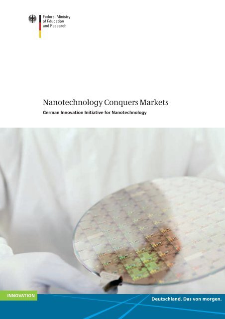
Nanotechnology Conquers Markets<br />
German Innovation Initiative for Nanotechnology
Imprint<br />
Published by<br />
Bundesministerium<br />
für Bildung und Forschung/<br />
Federal Ministry of Education and Research (BMBF)<br />
Publications and Website Division<br />
11055 Berlin<br />
Orders<br />
in writing to the publisher<br />
Postfach 30 02 35<br />
53182 Bonn<br />
or by<br />
phone: +49 (0) 1805 - 262 302<br />
Fax: +49 (0) 1805 - 262 303<br />
(0.12 Euro/min.)<br />
E-Mail: books@bmbf.bund.de<br />
Internet: http://www.bmbf.de<br />
Edited by<br />
BMBF, Referat 521<br />
VDI Technologiezentrum GmbH, Düsseldorf<br />
Authors<br />
Volker Rieke, BMBF<br />
Dr. Gerd Bachmann, VDI TZ GmbH<br />
Layout<br />
Suzy Coppens, Köln<br />
www.bergerhof-studios.de<br />
Printed by<br />
Druckhaus Locher GmbH, Köln<br />
Bonn, Berlin 2004<br />
Printed on recycled paper<br />
Photo credit, title page:<br />
Getty Images<br />
Photo: Stephen Derr
Nanotechnology Conquers Markets<br />
German Innovation Initiative for Nanotechnology
Contents<br />
4-5 Summary<br />
6 Nanotechnology – an interdisciplinary opportunity<br />
for innovations<br />
6-8 Nanotechnology in research and development<br />
9-12 Products and possible applications<br />
13-<strong>14</strong> Present situation in science, business<br />
and politics<br />
15 Players on the nanotechnology scene in Germany<br />
15 Project funding by the Federal Ministry of Education and Research (BMBF)<br />
16 Networks<br />
17-18 Institutional research establishments<br />
19 Universities and other research establishments<br />
19-20 Industrial R&D<br />
20 Nanotechnology funding in Germany<br />
21-22 German activities in comparison to other countries
23-25 Germany‘s innovation initiative for nanotechnology –<br />
New strategy for funding and support of<br />
nanotechnology by the BMBF<br />
26-27 Exploiting nanotechnology‘s market and employment potential through R&D<br />
28-33 Using leading-edge innovations for applications<br />
34 Creating research networks to promote innovation<br />
35 Acquiring, developing and safeguarding the fundamentals of the technical sciences<br />
36 Exploiting the opportunities for european and international cooperation<br />
37 Strengthening the role of SMEs<br />
37-38 Stabilizing new companies and encouraging established ones to relocate<br />
39 Promoting the young and developing qualifications<br />
39-40 Fostering young scientists<br />
41 Identifying qualification needs and developing expertise at an early stage<br />
42 Using opportunities for the good of society while avoiding risks<br />
42-43 Evaluating the social consequences<br />
44 Developing legal guidelines<br />
45 Evaluation<br />
46 Appendix<br />
46-47 Examples of objectives for the application of nanotechnology by relevant sector
4<br />
Summary<br />
Often described as the technology of the future,<br />
nanotechnology is attracting growing interest world-<br />
wide. Its distinguishing feature is that it gives rise to new<br />
functionalities solely as a result of the nanoscale<br />
dimensions of the system components — functionalities<br />
that lead to new and improved product properties.<br />
Because of this feature, and thanks to continually improving<br />
analytical and preparatory capabilities, nanotechnology has<br />
matured into a dominant focus of R&D activities in the last<br />
two decades. This new discipline will probably not only<br />
extend our ability to influence the properties of materials in<br />
specific ways, but also help us to better utilize them, and to<br />
integrate nanostructures into complex total systems. What’s<br />
more, it will do so to an extent that could be termed revolutionary.<br />
It does not, therefore, represent a basic technology<br />
in the classical sense — one with clearly defined parameters.<br />
Instead, it describes a new interdisciplinary approach that<br />
will help us to make further progress in the fields of biotechnology,<br />
electronics, optics and new materials.<br />
Nanotechnological advances do not serve as replacements<br />
for existing applications in these fields — their<br />
effect is rather to drive them to higher levels of functionality.<br />
In our everyday environments, we are surrounded by a<br />
broad spectrum of products that have already benefited<br />
from breakthroughs in nanotechnology. These include<br />
products as diverse as the hard disk drives in our computers,<br />
sunscreens with high UV protection factors and dirt-repellent<br />
surfaces in our showers. What’s more, interdisciplinary<br />
perspectives, particularly those spanning a range of<br />
industries, are opening up nanotechnology’s new potential<br />
for innovation — potential that could not be formulated in<br />
detail until now. This development represents a qualitative<br />
leap as far as the application and further commercial use of<br />
nanotechnology is concerned. As a result, the time has come<br />
to take concrete action and formulate research policy. The<br />
Summary<br />
race for the inside track as we strive to conquer the nanocosmos<br />
is already proceeding at top speed. Today the United<br />
States and Japan are investing enormously in this area — as<br />
are China, Korea and Taiwan. And the efforts of the latter<br />
three countries should not be underestimated. However, by<br />
establishing nanotechnology as an R&D priority of the EU’s<br />
Sixth Framework Programme (FP6), which began in 2002,<br />
the European Commission has responded to this competitive<br />
situation.<br />
The Federal Ministry of Education and Research<br />
(BMBF) faced up to this challenge early on. Even as far back<br />
as 1998, a supporting infrastructure plan was put in place<br />
with the establishment of six competence networks. That<br />
was in addition to increasing the BMBF’s collaborative<br />
project funding for this area. And although these measures<br />
did not receive the international recognition they warranted,<br />
they were implemented two years before the USA began<br />
its national initiative and four years before the European<br />
Union’s comparable measures in the Sixth Framework Programme.<br />
That is the reason why Germany is today Europe’s<br />
leading nation in the field of nanotechnology.<br />
To remain successful in the face of increasing globalisation,<br />
Germany must concentrate on its business and<br />
science know-how and make better use of these assets. An<br />
international comparison of the shares of publications and<br />
patents from the world’s nations shows that Germany’s work<br />
in the scientific domains of nanotechnology largely remains<br />
separated from application and product-orientated areas of<br />
R&D. In other words, there is still a lot of catching up to do in<br />
the area of industrial implementation. This is where the<br />
development of products and systems based on nanotechnological<br />
advances and the integration of nanostructures in<br />
microscopic and macroscopic environments present an<br />
opportunity that must not be missed. In many areas of nanotechnology,<br />
Germany is still out in front of many other countries<br />
in terms of knowledge. This know-how, together with<br />
the production and sales structures needed for implementation<br />
and Germany’s internationally renowned expertise in<br />
the area of systems integration, must be resolutely exploited<br />
in the marketplace.
This is exactly where the “German innovation initiative<br />
for nanotechnology” is taking up the challenge. On the<br />
basis of the white paper presented at the nanoDe congress in<br />
2002 and intensive discussions with representatives from<br />
business and science, the BMBF’s new approach to nanotechnology<br />
funding — starting from Germany’s highly-developed<br />
and globally competitive basic research in sciences and<br />
technology — primarily aims to open up the application<br />
potential of nanotechnology through research collaborations<br />
(leading-edge innovations) that strategically target the<br />
value-added chain. In addition, the BMBF is working to<br />
counteract the danger of a shortage of qualified scientists<br />
and technicians through its education policy activities. For<br />
many of Germany’s important industrial sectors — including<br />
the automotive business, IT, chemistry, pharmaceuticals and<br />
optics — the future competitiveness of their products depends<br />
on the opening up of the nanocosmos. Moreover,<br />
technology and innovation are increasingly becoming the<br />
deciding factors in the struggle to remain competitive in the<br />
face of the various challenges posed by low-wage countries.<br />
In other words, new technological trends such as nanotechnology<br />
will almost certainly have a powerful impact on the<br />
labour market of the 21st century — and thus on ensuring<br />
Germany’s continuing prosperity. Dawn has already broken<br />
on a new era characterized by the dynamic growth of nanotechnology;<br />
the challenge ahead is to set the course of future<br />
funding and to direct the breakthrough.<br />
The current overall strategy defines the framework<br />
for the BMBF’s new approach to nanotechnology funding in<br />
the future. The main elements of this strategy are:<br />
+ To open up potential markets and boost employment<br />
prospects in the field of nanotechnology<br />
• the green light will initially be given to<br />
funding for four leading-edge innovations<br />
(NanoMobil / automotive sector; NanoLux /<br />
optics industry; NanoforLife / pharmaceuticals,<br />
medical technology; and NanoFab /<br />
electronics)<br />
• “NanoChance”, a new BMBF funding<br />
measure for targeted support of R&Dintensive<br />
small and medium-sized enterprises,<br />
which offers existing companies assistance<br />
in the early stage of consolidation, will<br />
be established<br />
• the coordination between institutional<br />
BMBF funding — here especially with regard<br />
to synergy effects with the programmeorientated<br />
research of the HGF (Helmholtz<br />
Association) Centres and funding for nanosciences<br />
through the DFG (Deutsche Forschungsgemeinschaft)<br />
— and project support<br />
based on structural measures (networking,<br />
determining core topics, regular knowledge<br />
exchanges) will be optimised.<br />
+ Measures to support innovation will also be implemented<br />
to supplement these main elements. For the<br />
funding of young scientists, the “Junior Researcher<br />
Nanotechnology Competition” will be continued.<br />
The aim of this competition, which was founded in<br />
May 2002, is to recognize new innovative approaches<br />
at an early stage and to attract top young<br />
scientists who have emigrated abroad back to Germany.<br />
In addition, activities in the areas of standardization,<br />
patents, and training and further education<br />
will be launched.<br />
+ The dialogue on innovation and technology assessment<br />
will be actively pursued in order to give objectivity<br />
and thus direction to the partially critical public<br />
discussion about the opportunities and risks<br />
associated with nanotechnology. What’s more, the<br />
available results of three commissioned studies on<br />
innovation and technology assessment are evaluated<br />
in order to develop optional courses of action<br />
for the socially acceptable use of nanotechnology.<br />
5
6<br />
Nanotechnology — an<br />
interdisciplinary opportunity<br />
for innovations<br />
Nanotechnology in research<br />
and development<br />
Nanotechnology refers to the creation, investigation and application of structures, molecular materials, internal<br />
interfaces or surfaces with at least one critical dimension or with manufacturing tolerances of (typically) less than<br />
100 nanometres. The decisive factor is that the very nanoscale of the system components results in new functionalities and<br />
properties for improving products or developing new products and applications. These novel effects and possibilities result<br />
mainly from the ratio of surface atoms to bulk atoms and from the quantum-mechanical behaviour of the building<br />
blocks of matter.<br />
A nanometre (nm) equals one millionth of a millimetre. That<br />
corresponds roughly to the length of a chain of 5 to 10 atoms.<br />
By comparison, the cross-section of a human hair is 50,000<br />
times larger. However, a single atom or molecule does not<br />
Nanotechnology — an interdisciplinary opportunity for innovations<br />
Structuring with single atoms<br />
Source: Institut für Experimentelle und Angewandte Physik, Universität Kiel<br />
possess the properties we are familiar with, such as electrical<br />
conductivity, magnetism, colour, mechanical hardness or a<br />
specific melting point. On the other hand, even materials the<br />
size of a dust particle possess all of those physical properties
History<br />
The development of the scanning tunnel microscope<br />
(STM) in 1981 represented a milestone in the<br />
evolution of nanotechnology by providing the first<br />
direct access to the atomic world. In 1986 this achievement<br />
was honoured with the Nobel Prize in physics.<br />
Today, nanotechnology encompasses far more<br />
than the use of microscopes with atomic-scale<br />
resolution. Several nanomaterials with valuable<br />
innovative properties can already be manufactured<br />
on a large scale. Surfaces can be processed with<br />
nanoscale precision. And in specific instances, complex<br />
structures a few nanometres in size can already<br />
be created through self-organisation.<br />
As early as the mid-1980s, the Federal Ministry<br />
of Education and Research (BMBF) recognised<br />
that potential applications of nanotechnology were<br />
going to arouse intense discussion in all leading industrial<br />
nations, and that a remarkable increase in<br />
worldwide research activities would ensue. This insight<br />
resulted in sponsored projects starting in the<br />
early 1990s. To optimise the organisation of this<br />
increasingly complex field of technology, a supporting<br />
infrastructure in the form of competence<br />
centres was put in place starting in the late 1990s —<br />
in parallel with the funding of projects.<br />
Today, BMBF-sponsored nanotechnology<br />
projects alone encompass programmes in nanoelectronics,<br />
nanomaterials, optical technologies, microsystems<br />
engineering, biotechnology, communications<br />
technologies and production systems with a<br />
total budget amounting to about €100 million<br />
annually and increasing.<br />
— just as much as a steel object weighing tons. Nanotechnology,<br />
then, exists in the transitional range between individual<br />
atoms or molecules on the one hand and larger solid<br />
objects on the other. Phenomena that are not seen in macroscopic<br />
objects occur in this intermediate region. This interrelation<br />
of structural size and function makes it difficult to<br />
establish exactly what to include in the definition of nanotechnology.<br />
The following examples illustrate the new<br />
functionalities made available through nanotechnology:<br />
+ The increasing complexity of information technology<br />
creates a need for new nanoelectronic and<br />
optoelectronic components with capabilities based<br />
in part on quantum-mechanical effects.<br />
+ Structural sizes on the nanoscale alter the sensory<br />
properties of known materials to such an extent that<br />
new and more versatile sensors are created.<br />
+ Ultra-small particles can be used for new applications<br />
of paints and coatings. These include different<br />
colours due to controlled changes in particle size<br />
and endowing transparent coatings with specific<br />
functionalities such as dirt-repellent seals or UV<br />
protection.<br />
+ Minimal admixtures of nanomaterials produce substantial<br />
changes in solids. Plastic films, for instance,<br />
gain in tear strength, while ceramic materials become<br />
virtually unbreakable.<br />
+ The chemical reactivity and the useful life of catalysts<br />
can be substantially increased by means of making<br />
appropriate changes to the structure and composition<br />
of their surface.<br />
Such property changes are largely the result of a new<br />
approach in the utilisation of dimension, form and composition<br />
to achieve new functional principles of a physical,<br />
chemical and biological nature. Due to this trend towards<br />
integration, nanotechnology has evolved mainly along<br />
three routes that converge on the nanolevel.<br />
+ In recent decades, physico-technical methods have<br />
been the principal driver behind the generation of<br />
increasingly complex circuits and consequently<br />
smaller structures (top-down endeavours) in microelectronics.<br />
We can find off-the-shelf processors with<br />
ever faster clock speeds as well as memory components<br />
and disk drives with larger and larger capacities.<br />
Typical sizes of chip structures already reach<br />
below the 100-nm limit.<br />
7
8<br />
+ Insights from coordination chemistry and supramolecular<br />
chemistry have led to the deliberate<br />
creation of high-molecular, functional chemical<br />
compounds with enormous potential for applications<br />
in catalysis, membrane technology, sensing<br />
systems and thin-film technology (bottom-up<br />
endeavours).<br />
+ Very recently, our understanding of biological<br />
processes has been substantially expanded at both<br />
the cellular and molecular levels. This new knowledge<br />
includes many processes — such as the information<br />
flow from the gene to the protein, the selforganisation<br />
of molecules and photosynthesis —<br />
whose functionality and complexity has so far<br />
remained unattainable by technological means. In<br />
the future, the focus will be on applying the underlying<br />
biological principles more and more to technical<br />
systems. At the same time, biotechnology provides<br />
an ever larger toolbox of methods useful in<br />
designing customised, functional molecules that<br />
bring us within reaching distance of biologicaltechnical<br />
hybrid systems for such applications as<br />
implants, neurochips or artificial retinas.<br />
Most importantly, the methods of one discipline can be<br />
usefully complemented by processes and scientific insights<br />
from other fields. In examining nanoscale objects or in<br />
making specific structural changes, scientists generally use<br />
physical methods. The production of nanoscale particles, on<br />
the other hand, occurs primarily within the realm of<br />
chemistry. Nanoobjects such as structural proteins, enzymes<br />
and viruses, however, are created by self-organisation<br />
according to the laws of nature, and a large proportion of<br />
the basic processes, such as cellular energy generation<br />
processes (such as the respiratory chain or photosynthesis),<br />
occur on the nanoscale, i.e. at the molecular level.<br />
Bridging the gap between the macro, micro and<br />
nanoworlds is the task of system integration techniques. The<br />
required systems technologies include design and simulation<br />
tools and methods, assembly and joining technology,<br />
test methods, and appropriate production processes.<br />
Important demands on the assembly and joining technologies<br />
at the micro-nano interface include the realisation of<br />
the necessary mechanical, electromechanical or biochemical<br />
connections as well as the use of microsystems technology<br />
in the positioning and wiring of nanocomponents.<br />
General tendencies in the developement<br />
of nanotechnology<br />
Source: VDI Technologiezentrum GmbH
Products and possible applications<br />
Nanotechnology is increasingly contributing to the<br />
production of R&D-intensive products in the most diverse<br />
sectors of business. In many cases, successful product<br />
development is driven by the demand for extreme<br />
reductions in weight, volume, raw-materials utilisation<br />
and energy consumption, and by the need for speed.<br />
Nanotechnology is exceptional in that it often meets<br />
many of these criteria simultaneously.<br />
As a result, a boom of innovations is expected in virtually all<br />
high-technology industries, for example in information and<br />
communications technology, in automotive, power and<br />
production engineering, in the chemical and pharmaceutical<br />
industries and in medicine and biotechnology.<br />
The following are some examples of common<br />
products that are already benefiting from advances in<br />
nanotechnology and remain promising candidates for large<br />
markets.<br />
+ Every day we use computers, MP3 players, CD/DVD<br />
systems or mobile phones containing microchips,<br />
hard disks, RAM memory, diode lasers, displays,<br />
rechargeable batteries or new ceramic materials<br />
that have been optimised by the results of nanotechnology.<br />
+ LEDs in indicator panels, tail lights and flashlights<br />
convert electrical energy into light much more efficiently<br />
than incandescent bulbs while generating<br />
less heat.<br />
+ Nanometre-sized oxide particles endow sunscreen<br />
products with a high protection factor and are dermatologically<br />
safe. Such UV-absorbing nanoparticles<br />
are also used in some sunscreen fabrics, paints<br />
and lacquers, and in UV-reflecting films with<br />
potential new agricultural uses.<br />
+ Nanoparticles in protective coatings for household<br />
appliances, spectacle lenses, glazing materials for<br />
sanitary applications or in exterior house paints<br />
prevent scratches, tarnishing, smudging or algal<br />
growth.<br />
+ Chemical nanotechnology prevents fading of auto<br />
paints and protects them against scratches due to<br />
road dust.<br />
+ The daily vitamin pill would be ineffectual but for its<br />
nanoparticulate composition, which determines its<br />
solubility in water and thereby its availability to the<br />
human body.<br />
+ The admixture of natural nanoparticulate materials<br />
improves the absorbency of nappies and increases<br />
the tear strength as well as the airtightness of plastic<br />
wrap.<br />
These examples show that the current focus of R&D activities<br />
in the high-technology countries tends to be on improving<br />
products in already established applications in order to make<br />
them more competitive. To a large extent, the production<br />
of typical “nanoproducts” must still await the completion of<br />
basic research, and that is projected to require several years,<br />
and in some cases decades.<br />
Society will then be able to enjoy the prospects of<br />
increased environmental compatibility of lifestyle and<br />
mobility, drastically improved communications and information<br />
as well as optimised healthcare. Nanotechnology<br />
can contribute to better quality of care at less cost in an<br />
aging society through improved and more economical<br />
diagnostic and treatment methods, including nanostructured<br />
biochips, nanoprobes, intelligent depot medications<br />
for sustained release, microsystems to complement organic<br />
functions, and artificial substrate materials for tissue<br />
implants.<br />
9
10<br />
Even today it is possible to envision examples of<br />
future applications in these areas that are likely to benefit<br />
substantially from the advances in nanotechnology.<br />
+ Automotive engineering is pursuing applications to<br />
which nanotechnology can make a significant<br />
contribution. In this quest, new technical refinements<br />
are useful both functionally (minimised fuel<br />
consumption, driving safety, long product life) and<br />
cosmetically (e.g. switchable paints). The car of the<br />
future will respond intelligently both to environmental<br />
stimuli and to driver behaviour. Windows<br />
and mirrors will adjust to exterior lighting. Tyres will<br />
have good traction on the most diverse road surfaces.<br />
And multiple sensors will proactively adjust<br />
the driving condition to a change in weather or an<br />
impending collision. Switchable colour changes in<br />
the paint and easier modifications using lightweight<br />
designs will allow customised styling. New knowledge<br />
in nanotechnology will contribute to optimised<br />
combustion and emission control, a reduction in<br />
body weight, the development of self-healing paint,<br />
wear-resistant tyres with good road grip, and functional<br />
window glass. Electronics already contribute a<br />
disproportionately large share to the added value in<br />
automobile manufacturing. The importance of automotive<br />
electronics will continue to grow and, in<br />
keeping with the auto industry’s role as a technology<br />
driver, spur on the development of nanoelectronic<br />
innovations into marketable products.<br />
+ Machine and plant construction contributes to the<br />
advancement of nanotechnology applications in<br />
two different contexts. On the one hand, this<br />
discipline makes new manufacturing and systems<br />
technologies available (methods for producing<br />
Current status of nanotechnology and some application fields illustrated by examples.<br />
The timeline for the introduction into the market is in some cases no more than a kind<br />
of educated guessing. Forecasting the fate of developements at the time of their onset is<br />
especially risky.<br />
Source: VDI Technologiezentrum GmbH
nanostructures, ultra-precision processing, systems<br />
for nanobiotechnology and nanochemistry). On the<br />
other, the use of nanostructures in function-determining<br />
layers, in measuring instruments and in<br />
sensing systems makes it possible to design better<br />
machines and plants. As a result, the productivity<br />
and reliability of machines and plants is increased,<br />
making this traditionally strong German industry<br />
and its products even more competitive.<br />
+ The development of highly efficient or even autonomous<br />
power supplies for portable devices is an<br />
urgent priority in power engineering. Disposable as<br />
well as rechargeable batteries continue to be unsatisfactory<br />
with respect to weight and performance.<br />
But a combination of economical electrical and<br />
electronic components, efficient lighting and display<br />
systems, and above all innovative energy storage<br />
devices such as small-format fuel cells is expected<br />
to provide new solutions. What’s more, integrated<br />
energy converters based on nanotechnology,<br />
such as highly efficient solar cells or innovative materials<br />
that directly convert heat into electricity<br />
(thermoelectric materials) may provide a replacement<br />
for rechargeable batteries in low-power<br />
EUVL stepper for the IC fabrication<br />
Source: Carl Zeiss SMT AG<br />
applications. That would give an enormous boost to<br />
products such as portable electronics and diagnostic<br />
systems (wearable electronics).<br />
+ In medicine, the focus continues to be on diagnostic<br />
and therapeutic approaches for managing widespread<br />
diseases such as cancer and diabetes. In this<br />
field, nanoparticles represent a new platform<br />
technology. They can be accumulated in the tumour<br />
as a selective contrast medium for medical imaging,<br />
or destroy tumour tissues locally by heating them,<br />
or, even more importantly, by transporting specifically<br />
effective therapeutic agents. In the long term,<br />
these particles also appear to point the way to noninvasive<br />
methods for early diagnosis. What’s more,<br />
these techniques will be complemented by diagnostic<br />
applications of biochips produced by nanoand<br />
microsystems technology. A virtual boom is<br />
already under way in the use of these chips in pharmaceutical<br />
research and laboratory applications.<br />
The expansion of biochip technologies brings us a<br />
significant step closer to the distant goal of individualised<br />
medicine, in which prompt on-site diagnostics<br />
will be complemented by customised<br />
medications. The first drug delivery systems for<br />
11
12<br />
transporting chemotherapeutic agents to the<br />
tumour are now close to being approved.<br />
+ In the field of information and communications, the<br />
availability of any desired information, any time,<br />
anywhere in the world, would be an objective toward<br />
which nanotechnologies, and especially nanoelectronics,<br />
can make a significant contribution. In<br />
the future one should be able to use a device of<br />
negligible size (comparable to a wristwatch, say) to<br />
access any required information, or to communicate<br />
with any desired party. In such devices, the information<br />
should not merely appear as a string of<br />
characters on a tiny display. Instead, the user should<br />
be able to select the preferred presentation from a<br />
diversity of processed formats, ranging perhaps<br />
from text-to-speech all the way to three-dimensional<br />
holographic images. These devices would provide<br />
medical on-line diagnostic capability with automatic<br />
alerts, and their data storage would have the<br />
capacity of a national library. The computing power<br />
Nanosystems in our future life<br />
Source: Siemens AG<br />
Artificial hip joints<br />
made by biocompatible<br />
materials<br />
Fuel cells deliver electricity<br />
for mobiles and cars<br />
Intelligente clothings<br />
measure pulse and<br />
breathing frequency<br />
Buckytube-frame is<br />
lightweight and tough<br />
of such an “electronic assistant” would rival that of<br />
a present-day computing centre.<br />
+ In optics too, developments are opening up a wide<br />
range of potential future products. Optoelectronic<br />
components already play an important part in home<br />
entertainment (CD/DVD, laser TV, projection systems,<br />
optical interconnects) and will continue to<br />
grow in importance, as will lighting technologies<br />
based on optoelectronic components, such as largearea<br />
light-emitting diodes (LEDs). Due to their long<br />
service life and high efficiency, optoelectronic light<br />
sources are not only more reliable than conventional<br />
light sources; they also consume much less energy<br />
and are therefore more cost-efficient. What’s more,<br />
optical lenses of any desired geometry and manufactured<br />
with nanometre precision will be used for<br />
highly precise, function-specific conduction and deflection<br />
of light in applications such as data equipment<br />
and (home) cinema projectors, lithography or<br />
medical systems.<br />
OLEDs for displays<br />
Scratch resistant window<br />
glass cleans itself with a<br />
lotus effect<br />
Light emitting diodes<br />
compete with conventional<br />
bulbs<br />
Nanotubes for new<br />
notebook-displays
Present situation in science, business and politics<br />
Present situation in<br />
science, business and<br />
politics<br />
During the course of the past decade, advances in our understanding of quantum effects, boundary properties and surface<br />
properties, as well as of the principles of self-organisation, have laid the foundations for innovative analytical and<br />
production techniques which have caused an upsurge of interest in nanotechnology and global networking activities along<br />
the value-added chain.<br />
This interest has been boosted in particular by the early<br />
combination of basic research results and application<br />
options, and by the resulting expectations regarding potential<br />
markets. The players on Germany’s nanotechnology<br />
scene were among the world’s first to address potential<br />
applications at an early stage, on the basis of solid and<br />
broad-based fundamental research. More than 100 companies<br />
in Germany have already recognised these innovation<br />
opportunities and are using nanotechnology knowhow<br />
in their core business. Today, a total of about 400 to 500<br />
companies in Germany are involved with nanotechnology<br />
and are becoming increasingly active in this field as product<br />
developers, suppliers or investors. These companies do not<br />
view nanotechnological R&D work as a short-lived fashion<br />
but are taking a long-term approach in addressing key<br />
elements for future innovation in industries with a large<br />
job-creation potential, primarily in the automotive and machine-construction<br />
industries, in chemicals and pharmaceuticals,<br />
in the optical industry, medicine and biotechnology,<br />
as well as in power generation and construction. Many<br />
small and medium-sized enterprises (SMEs) that can be ranked<br />
as pure nano businesses have sprung up in Germany.<br />
These flexible innovation companies occupy specific niches<br />
in the value-added chain and make an important contribution<br />
to know-how transfer from research to industry.<br />
SMEs consequently serve a key function in most high-technology<br />
fields, and establishing innovative start-ups is therefore<br />
of enormous importance in the young nanotechnology<br />
industry too.<br />
13
<strong>14</strong><br />
Source: Flad&Flad Communication GmbH
Players on the nanotechnology scene<br />
in Germany<br />
The success of nanotechnology in Germany is based on<br />
a large cast of players in business, science and govern-<br />
ment — in other words, on a substantial public and priva-<br />
te commitment.<br />
Project funding by the Federal Ministry of<br />
Education and Research (BMBF)<br />
Table 1: : Expenditures on nanotechnology within various BMBF core topic areas<br />
BMBF nanotechnology funding Core topic areas 1998 2002 2003 2004 2005<br />
(in million €)<br />
Nanomaterials Nanoanalytics, nanobiotechnology,<br />
nanostructured materials, nanochemistry,<br />
CCN, new “nano talent“<br />
recruting, nano opportunity<br />
19,2 20,3 32,7 38,1<br />
Production technologies Ultrathin films, ultraprecise<br />
surfaces<br />
0,2 0,8 2,2 2,2<br />
Optical technologies Nanooptics, ultraprecision processing,<br />
microscopy, photonic crystals,<br />
molecular electronics, diode lasers,<br />
OLEDs<br />
18,5 25,2 26,0 26,0<br />
Microsystems technology Systems integration, nano-sensors,<br />
nano-actors, energy systems<br />
7,0 7,0 9,4 10,2<br />
Communications technologies Quantum structure systems,<br />
photonic crystals<br />
4,3 4,0 3,6 3,4<br />
Nanoelectronics EUVL, lithography,<br />
mask technology, e-biochips,<br />
magnetoelectronics, SiGe electronics,<br />
19,9 25,0 44,7 46,2<br />
Nanobiotechnology Manipulation technologies, functionalised<br />
nanoparticles, biochips,<br />
4,6 5,4 5,0 3,1<br />
Innovation and technology analyses ITA studies 0,2 0,5 0,2<br />
Total (in million €) 27,6 73,9 88,2 123,8 129,2<br />
Since the late 1980s, the BMBF has been funding nanotechnology<br />
research activities in the contexts of its Materials<br />
Research and Physical Technologies programmes. Initial<br />
core topic areas included the production of nanopowders,<br />
the creation of lateral structures on silicon and the development<br />
of nanoanalytical methods. BMBF support was later<br />
expanded to also include other programmes with relevance<br />
to nanotechnology, for instance in the Laser Research and<br />
Optoelectronics programmes. Today, many projects related<br />
to nanotechnology are supported through a considerable<br />
number of specialized programmes. Examples include<br />
Materials Innovations for Industry and Society (WING), IT<br />
Research 2006, the Optical Technologies Sponsorship<br />
Programme and the Biotechnology Framework Programme.<br />
From 1998 to 2004, the volume of funded joint projects in<br />
nanotechnology has quadrupled to about €120 million.<br />
Table 1 lists BMBF expenditures on nanotechnology research<br />
in various core topic areas for the fiscal years 1998 and 2002<br />
to 2005.<br />
In addition to BMBF-funded research, project-related<br />
investments are also financed by the Ministry of Economics<br />
and Employment (BMWA) in the Physikalisch-Technische<br />
15
16<br />
Bundesanstalt (PTB — the national metrology institute) and<br />
the Federal Institute for Materials Research and Testing<br />
(BAM), as well as nanotechnology-related projects in the PRO<br />
INNO innovation competency programme for SMEs. These<br />
projects are funded to the tune of about € 25 million<br />
annually.<br />
Networks<br />
BMBF-funded competence centres (CCN)<br />
In 1998, the BMBF established six competence centres with<br />
an annual funding of approx. €2 million. In Phase 3, starting<br />
in the autumn of 2003, nine competence centres have begun<br />
or continued their work as nationwide, subject-specific<br />
networks with regional clusters in the most important areas<br />
of nanotechnology:<br />
+ Ultrathin functional layers (Dresden)<br />
+ Nanomaterials: Functionality by chemistry<br />
(Saarbrücken)<br />
+ Ultraprecise surface processing (Braunschweig)<br />
+ Nanobioanalytics (Münster)<br />
+ HanseNanoTec (Hamburg)<br />
+ Nanoanalytics (München)<br />
+ Nanostructures in optoelectronics — NanOp (Berlin)<br />
+ NanoBioTech (Kaiserslautern)<br />
+ NanoMat<br />
(Karlsruhe; established and financed by the FZK)<br />
The purpose of the infrastructural activity of these competence<br />
centres is to optimise the conditions for bringing<br />
potential users and nanotechnology researchers together.<br />
The centres will efficiently focus the nanotechnological<br />
knowledge of their members and convert it into industrial<br />
development. Other tasks of the competence centres include<br />
in particular activities related to training and continuing<br />
education, collaboration on issues concerning standardisation<br />
and regulations, consulting and support of would-be<br />
entrepreneurs and public-relations work. The individual<br />
competence centres are organised along the subject-specific<br />
value-added chain in their respective fields. The entire<br />
network presently interlinks approximately 440 players<br />
from the academic sphere (29%), research institutions (23%),<br />
large corporations (12%), small and medium-sized enterprises<br />
(31%) as well as financial services, consultants and<br />
associations (totalling 5%). The information sharing supported<br />
by the competence centres is particularly helpful for<br />
small companies to keep them informed about current<br />
developments and what such developments mean to them.<br />
In the next three years, the centres intend to focus especially<br />
on training and continuing education, and on supporting<br />
start-up companies. In the future, BMBF funding will also be<br />
complemented by regional financing through the Federal<br />
States to the same amount.<br />
CCN evaluation results:<br />
+ Successful integration of several scientific and<br />
technical disciplines<br />
+ Established forum for science and industry<br />
+ Established a nano discipline<br />
+ Networks along the value-added chain<br />
+ Achieved international visibility<br />
+ Primary contact for interested parties<br />
+ Accelerated the innovation process<br />
Other networks<br />
Besides the competence centres that are directly supported<br />
by the BMBF, several other networks have evolved that<br />
pursue different goals and are therefore differently<br />
structured.<br />
In contrast to networks with a (virtual) structure that<br />
is generally nationwide, several universities and research<br />
centres have consolidated their nanotechnological basic<br />
research activities through local — in some cases even<br />
internal — networks. Examples include:<br />
+ CeNS (München),<br />
+ CINSAT (Kassel),<br />
+ CNI (Jülich)<br />
+ CFN (Karlsruhe).<br />
The NanoBioNet in the Saarland region also has a strong<br />
regional focus.The establishment of incubators founded by<br />
universities plays a very special part by supporting spin-offs<br />
in the academic environment. To meet this objective,<br />
CenTech GmbH in Münster, for example, has established its<br />
own start-up support centre.
Institutional research establishments<br />
Institutional nanotechnology funding (in million €) 2002 2003 2004 2005<br />
Deutsche Forschungsgemeinschaft (DFG} 60,0 60,0 60,0 60,0<br />
Wissensgemeinschaft G.W. Leibniz (WGL) 23,7 23,6 23,4 23,5<br />
Helmholtz-Gemeinschaft (HGF) 38,2 37,1 37,4 37,8<br />
Max-Planck-Gesellschaft (MPG) <strong>14</strong>,8 <strong>14</strong>,8 <strong>14</strong>,8 <strong>14</strong>,8<br />
Fraunhofer-Gesellschaft (FhG) 4,6 5,4 5,2 4,9<br />
Caesar 1,8 3,3 4,0 4,4<br />
Total (in million €) <strong>14</strong>3,1 <strong>14</strong>4,2 <strong>14</strong>4,8 <strong>14</strong>5,4<br />
In Germany, institutional research in nanotechnology<br />
outside the universities is pursued by the four large research<br />
associations: MPG, FhG, HGF and WGL. These associations<br />
maintain numerous research establishments or working<br />
groups whose range of activities includes nanotechnology<br />
research. What’s more, these partners are also integrated<br />
into many collaborative research programmes and priority<br />
programs of the DFG. Table 2 lists the public expenditures on<br />
nanotechnology-related research in DFG funded projects,<br />
and expenditures on institutional support by the BMBF<br />
jointly with the Federal States.<br />
Fire protection materials with nanoscaled fillers<br />
Source: Institut für Neue Materialien, Saarbrücken<br />
Table 2: Funds for nanotechnology research in the context of DFG funding and<br />
institutional funding.<br />
Wissenschaftsgemeinschaft<br />
G. W. Leibniz (WGL)<br />
The institutes of the WGL (G.W. Leibniz Science Association)<br />
conduct basic and industrially orientated work in nanotechnology.<br />
Some of their principal efforts are focused on<br />
nanomaterials research, in which the Institutes for New<br />
Materials (INM , Saarbrücken), for Solid State and Materials<br />
Research (IFW, Dresden) and for Polymer Research (IPF,<br />
Dresden) rank among the leaders; and on surface technology,<br />
for instance at the Institute for Surface Modification<br />
(IOM, Leipzig) and at the Rossendorf Research Centre (FZR).<br />
Work at the Paul-Drude-Institut (PDI, Berlin) includes basic<br />
research in solid state electronics.<br />
The INM is strictly a nanotechnology centre. In addition<br />
to the application-related development of new<br />
nanomaterials with heat-resistant, anti-reflecting,<br />
electrochromic, self-cleaning and other properties,<br />
the institute is also engaged in technology transfer.<br />
Several start-up companies are already doing business<br />
as spin-offs of the INM. The INM develops processing<br />
and manufacturing methods for diverse nanomaterials<br />
up to and including readiness for actual<br />
use (including contract development on behalf of<br />
industry).<br />
17
18<br />
Helmholtz-Gemeinschaft deutscher Forschungszentren<br />
(HGF)<br />
The HGF (Helmholtz Association of National Research<br />
Centres) also conducts work on issues related to materials<br />
and nanoelectronics. Especially noteworthy is the work at<br />
the two research centres in Karlsruhe (FZK) and Jülich (FZJ).<br />
R&D on nanomaterials and thin-film systems is also pursued<br />
at the research centre in Geesthacht (GKSS) and at the<br />
Hahn-Meitner-Institut in Berlin (HMI).<br />
At the FZK, the research field “Key Technologies —<br />
NANO” focuses on two subjects: nanoelectronics<br />
and nanostructured materials. The Centre has<br />
moreover joined the Universities of Karlsruhe and<br />
Strasbourg in establishing the NanoValley research<br />
association. This research is conducted at the newlybuilt<br />
Institute for Nanotechnology (INT) of the FZK.<br />
Max-Planck-Gesellschaft (MPG)<br />
Work at the institutes of the MPG (Max Planck Society) is<br />
contributing fundamentally important knowledge towards<br />
new approaches in nanotechnology research. The<br />
Institute for Solid State Research and Metals Research in<br />
Stuttgart and the MPI for Microstructure Physics in Halle<br />
for instances have been active for many years in the fields<br />
of nanomaterials, characterisation methods and new<br />
functionalities. Internationally recognized R&D achievements<br />
have also been contributed by the Institutes for<br />
Polymer Research (Mainz), for Colloid and Boundary Layer<br />
Research (Golm), for Biochemistry (Munich-Martinsried),<br />
for Coal Research (Mülheim), and by the Fritz-Haber<br />
Institute (Berlin).<br />
The MPI for Solid State Research emphasizes close<br />
collaboration between the different disciplines of<br />
physics and chemistry as well as between experimentally<br />
and theoretically active scientists. The<br />
centre conducts nanoresearch and technology<br />
particularly in the following areas: nanoionics, carbon<br />
nanotubes, nm-thin films, barrier layers and<br />
nanoparticles.<br />
Animal cell (fibroblast) on a nanostructured substrate<br />
Source: Fraunhofer IBMT, St. Ingbert<br />
Fraunhofer Gesellschaft (FhG)<br />
Since an industrial demand already exists in most areas of<br />
nanotechnology, many institutes of the FhG (Fraunhofer<br />
Society) conduct projects focused on specific applications<br />
jointly with industrial companies. Some of these efforts are<br />
focused on thin-film and surface technologies, a field in<br />
which the FhG has been supported by the BMBF for many<br />
years. The Institutes for Materials and Laser Beam Technology<br />
(IWS, Dresden), for Silicate Research (ISC, Würzburg),<br />
for Optics and Precision Mechanics (IOF, Jena) and for<br />
Boundary Layer Research (IGB, Stuttgart) have been very<br />
active in this subject area. Nanomaterials research receives<br />
high priority at the Institutes for Applied Materials Research<br />
(IFAM, Bremen), for Applied Solid State Physics (IAF, Freiburg)<br />
and for Chemical Technology (ICT, Pfinztal), among<br />
others. The Institutes for Silicon Technology (ISIT, Itzehoe)<br />
and for Production Technology (IPT, Aachen) are exploring<br />
the interface of microtechnology and nanotechnology. The<br />
Fraunhofer Institute for Reliability and Microintegration<br />
(IZM, Berlin) is making contributions in particular to assembly<br />
and interconnection technology. The Institute for Biomedical<br />
Technology (IBMT, St. Ingbert) is exploring links to<br />
nanobiotechnology. The Institute for Solar Energies (ISE,<br />
Freiburg) is investigating the contribution of nanotechnology<br />
to energy production.<br />
The FhG-IBMT conducts nanobiotechnology<br />
research. The principal research areas here are<br />
biosensor systems and biochip research. Specific<br />
research subjects include, among others, biosensing<br />
technology, biohybrid systems, molecular<br />
bioanalytics and bioelectronics, as well as medical<br />
biotechnology & biochip technology.
Universities and other research establishments<br />
Nearly all German universities with a technical and scientific<br />
programme of studies are conducting R&D related to<br />
nanotechnology. At the same time, growing emphasis is<br />
given to developing an interdisciplinary understanding of<br />
the relationships in various areas of this field. At several<br />
universities, nanotechnology courses of study have already<br />
been established that are closely linked to current research<br />
topics. Examples of the comprehensive activities covering<br />
this subject area can be found in the academic centres of<br />
Karlsruhe, Aachen, München, Münster, Hamburg, Saarbrükken,<br />
Kaiserslautern, Berlin, Kassel, Würzburg, Freiburg and<br />
Marburg. Technical universities too are beginning to focus<br />
more sharply on this field of studies.<br />
In addition to the aforementioned institutes, the<br />
strongly diversified R&D system in Germany also includes<br />
other establishments involved with nanotechnology, such as<br />
the NMI in Reutlingen, AMICA Aachen, IMS-Chips in<br />
Stuttgart, FBH Berlin, Bessy II Berlin, PTB Braunschweig,<br />
CAESAR in Bonn and IPHT in Jena.<br />
Courses of study in nanotechnology<br />
+ Nanostructure Technology (University of<br />
Würzburg)<br />
+ Nanostructure Sciences (University of Kassel)<br />
+ Micro- and Nanostructures (Saarland University)<br />
+ Bachelor Course Nanoscience (University Bielefeld)<br />
+ Molecular Science (University Erlangen-Nürnberg)<br />
+ Nanomolecular Science (International University<br />
Bremen)<br />
+ Master‘s Programme in Micro- and Nanotechnology<br />
(FH München)<br />
+ Bio- and Nanotechnologies (FH Südwestfalen)<br />
Industrial R&D<br />
The players in the nanotechnology field in Germany also<br />
include several hundred industrial companies. Research<br />
programmes in many large corporations such as Infineon,<br />
DaimlerChrysler, Schott, Carl Zeiss, Siemens, Osram,<br />
Degussa, BASF, Bayer, Metallgesellschaft and Henkel include<br />
open questions in nanotechnology. For example, nearly all<br />
major chemical companies are working with nanoscale<br />
materials. These research activities vary in the way they are<br />
organised. While Henkel has spun off SusTech and Phenion<br />
in cooperation with the universities in Darmstadt and<br />
Frankfurt for the development and marketing of new<br />
nanotechnology applications outside the company in a<br />
university setting, Degussa has launched “Projekthaus<br />
Nano” at Creavis, a wholly-owned subsidiary, to research<br />
nanotechnological methods and products in-house to the<br />
point of their suitability for application with the support of<br />
universities. Some of these developments are currently<br />
being transferred to business units.<br />
Carl Zeiss was established back in 1846 and has<br />
always been engaged in subjects related to<br />
precision mechanics and optics. The company is<br />
world-renowned, especially in the field of ultraprecision<br />
processing. To serve the field of<br />
lithography more efficiently, the company<br />
established Carl Zeiss Semiconductor<br />
Manufacturing Technologies AG as a spin-off on a<br />
new manufacturing site.<br />
A third available model is to entirely outsource the<br />
utilisation of the research results and of any related patents.<br />
Examples include spin-offs such as Sunyx (from Bayer AG)<br />
and Mildendo (from Jenoptik). Infineon AG is using yet<br />
another model to implement nanotechnology knowledge,<br />
by assigning responsibility for this area to an internal<br />
research department (Infineon-CPR Corporate Research)<br />
with a distinct focus on nanotechnology. In addition to sub-<br />
50-nm CMOS transistors for future nanoelectronics this<br />
organisation is also focusing on carbon nanotubes (CNTs) as<br />
possible connections between different chip levels (chip<br />
interconnects).<br />
While large companies tend to be interested mainly<br />
in system solutions with prospects of large sales volumes,<br />
small and mid-sized enterprises are mainly concerned with<br />
production, analysis and equipment-related technologies.<br />
SMEs in this field include Nanogate Technologies GmbH<br />
(Saarbrücken), a company that supplies its nanomaterials for<br />
a variety of applications (easy-to-clean coatings, non-stick<br />
products, anti-graffiti protection, etc.). HL-Planar, a company<br />
that manufactures various sensors and also provides<br />
services in the field of thin-films for microsystems, is already<br />
using nanotechnology under a variety of conditions in manufacturing<br />
GMR sensors for the auto and machine-construction<br />
industry. Important players in nanotechnology in<br />
Germany also include many start-up companies (spin-offs of<br />
universities and research institutes) such as Nano-X, ItN-<br />
Nanovation, NanoSolution, Capsulution and so on. In<br />
addition to companies specialising in the production of<br />
nanomaterials, there are many others that are active in<br />
nanostructuring (such as Aixtron, NaWoTec, Team<br />
Nanotech, Nanosensors) or nanoanalytics (including<br />
Omicron Nanotechnologies, IoNTOF, NanoAnalytics,<br />
Nanotype, SIS and NanoTools).<br />
19
20<br />
In the early 1980s, Omicron Nanotechnologies<br />
GmbH was already addressing subjects that<br />
became important in nanotechnology during the<br />
following years: analytics and coating methods.<br />
Soon after the discovery of the scanning tunnel<br />
microscope, Omicron began to focus on the<br />
manufacture of such instruments and broadened its<br />
line of microscopy and analytical instruments to<br />
such an extent that, from the mid-1980s on, it<br />
achieved an annual growth rate of about 25%.<br />
Today, the company is the global market leader in<br />
scanning tunnel microscopy systems for research.<br />
Nanotechnology funding in Germany<br />
Not counting the industry’s own contribution, Germany’s<br />
public expenditures for nanotechnology funding in 2004<br />
total about € 290 million. This does not include the Federal<br />
States’ expenditures on the universities’ basic budgets, nor<br />
the industry’s own funding of nanotechnology research<br />
apart from public funding.<br />
Surface with hydrophobic properties<br />
Source: BASF AG<br />
Evaluation of the nanotechnology player scene<br />
in Germany<br />
In the field of nanotechnology, Germany can build<br />
on a well-educated corps of scientists, on a differentiated<br />
and networked R&D and industrial<br />
landscape, and on committed engineers and<br />
entrepreneurs. All of these players are aware that<br />
nanotechnology innovations require large investments<br />
but that they also create new job opportunities.<br />
The BMBF supports such innovative companies<br />
by funding collaborative projects, particular<br />
in those applications in which a dominant market<br />
position and high profit targets appear attainable.<br />
Both these forward-looking companies and public<br />
institutions are investing substantial sums in<br />
strengthening this discipline and the players in it.<br />
These efforts include both R&D work and an expanding<br />
array of supporting measures, such as the<br />
development of networked structures, the establishment<br />
of academic programmes in nanotechnology<br />
and other activities designed to ensure a<br />
pool of new talent, as well as the familiarisation of<br />
society with this subject.<br />
Table 3: Public expenditure on funding for nanotechnology projects in Germany.<br />
Nanotechnology funding in Germany (in million €) 2002 2003 2004 2005<br />
BMBF project funding 73,9 88,2 123,8 129,2<br />
BMWA project funding 21,1 24,5 24,5 23,7<br />
Institutional funding <strong>14</strong>3,1 <strong>14</strong>4,2 <strong>14</strong>4,8 <strong>14</strong>5,4<br />
Total (in million €) 238,1 256,9 293,1 298,3
German activities in comparison to<br />
other countries<br />
In developing basic requirements for new products and<br />
applications, Germany ranked among the top contenders<br />
worldwide in most technology sectors, and in nano-<br />
technology R&D Germany is also considered to be at the<br />
same level as the USA and Japan.<br />
But a comparison of different countries’ shares in the volume<br />
of publications and patents reveals that a gulf still separates<br />
the realm of nanotechnology science in Germany from<br />
applications- and product-orientated R&D. In this respect<br />
the situation is more comparable with that in Japan, while<br />
the USA is pursuing objectives that are much more implementation-orientated.<br />
Germany is strong in the nanosciences, but it still has<br />
some catching up to do in their industrial implementation.<br />
As fascinating as the opportunities in<br />
nanotechnology are, German industrial customers<br />
and others in this market still appear hesitant to<br />
seize and use them for innovative products.<br />
Despite its excellence as a research location, its numerous<br />
start-up companies and its market opportunities, Germany<br />
still has some catching up to when it comes to implementing<br />
its nanotechnology expertise. To end this state of affairs and<br />
lay the foundation for future competitiveness, the BMBF has<br />
turned to a new approach by establishing competence<br />
centres, opening new avenues of support for SMEs and<br />
supporting concurrent educational initiatives. This new,<br />
parallel strategy — the funding of projects concurrent with<br />
the establishment of a supporting infrastructure — has<br />
reinforced Germany’s position among the top contenders in<br />
nanotechnology research while increasing the number and<br />
enhancing the reputation of companies involved with<br />
nanotechnology. In approximate terms, both the USA and<br />
Europe have about the same number of companies involved<br />
in nanotechnology. Roughly half of the companies located<br />
in Europe originate in Germany.<br />
A comparison with the situation in Japan or other<br />
countries in Southeast Asia is difficult due to the lack of<br />
reliable company data for that region. Based on rough<br />
estimates and without further analysis of the details of the<br />
provided support, a comparison of expenditures in Europe,<br />
the USA and Japan shows very similar levels of funding.<br />
During the 2002 fiscal year, around € 570 million was spent<br />
in the USA and approx. € 770 million was approved for 2003.<br />
Japan’s “Governmental Budget Plan for Nanotechnology”<br />
includes a total of € 750 million for 2002 and provides € 800<br />
million annually starting in 2003. Recently the British<br />
government has announced an initiative to guarantee<br />
expenditures amounting to approx. € 130 million, starting in<br />
2004, for the next six years. The Research Directorate<br />
General of the European Commission estimates funding for<br />
nanotechnology in Europe to add up to approx. € 700<br />
Table 1: Expenditures for the support of nanotechnology in Germany, Europe, the USA<br />
and Japan in millions of euros (for simplicity’s sake, $1 is assumed to equal € 1 and 100<br />
yen; for comparison purposes these data are questionable, because there is no<br />
internationally uniform definition of the field, the data differ with respect to gross or<br />
net expenditures, purchasing power differences are not considered, and it is virtually<br />
impossible to accurately state industrial expenditures.)<br />
(in million €) 2001 2002 2003 2004<br />
Germany 210 240 250 290<br />
Europe<br />
(incl. nat. funding)<br />
360 480 700 740<br />
USA 420 570 770 850<br />
Japan 600 750 800 800<br />
21
22<br />
million in 2003. The European Commission has budgeted a<br />
sum of € 700–750 million for the period ending in 2006 — in<br />
other words, about € 250 million annually starting in 2003<br />
— through the funding activities of the Sixth Framework<br />
Programme (FP6), in which nanotechnology is primarily<br />
supported under the 3rd Thematic Priority. Germany is also<br />
participating with approximately € 250 million annually,<br />
which makes it the largest contributor in public funding of<br />
nanotechnology in Europe. Consequently, a total of about<br />
€ 200-250 million for nanotechnology R&D can be considered<br />
realistic for the other member nations as a whole.<br />
Today, nanotechnology is recognised as an important<br />
field for the future in all relevant industrial nations and<br />
is funded accordingly. As a result, national or region-specific<br />
research programmes are being established not only in the<br />
USA, in Japan and Europe but also in China, Korea, Taiwan,<br />
Australia and other countries. What the current programmes<br />
in nearly all of these countries have in common (besides<br />
the large investments in this future technology) are attributes<br />
that were addressed by the BMBF five years ago:<br />
+ An interdisciplinary approach in supporting this<br />
field<br />
+ Simultaneous support of basic and applied research<br />
+ Initiation of networking activities<br />
+ Expansion of international cooperation<br />
+ Combination with issues of future training and<br />
continuing education<br />
+ Public discussion of socially relevant questions<br />
+ The demand for rapid knowledge conversion in<br />
order to strengthen local economies<br />
Summing up the present situation<br />
During the past several years, nanotechnology-related<br />
measures launched by the BMBF have substantially increased<br />
the visibility of the activities in Germany. According<br />
to Philippe Busquin (Research Commissioner of the EU)<br />
“Germany is the growth engine in the EU with respect to<br />
nanotechnological innovations.” This statement is an indicator<br />
that Germany is well positioned in nanotechnology,<br />
both scientifically and infrastructurally. The BMBF has<br />
initiated the development of this future technology earlier<br />
than has been the case in other countries and has appropriately<br />
addressed the scope of this subject in several technical<br />
programmes. An internationally recognised position has<br />
been established in specific areas by focusing on industryorientated<br />
issues. This position must now be reinforced and<br />
expanded by appropriate additional actions. To prevail in<br />
the face of a strong upsurge of international competition,<br />
the speed of the innovation process must be increased and<br />
the long-term creation of added value must be ensured by<br />
measures that are supportive of innovation.<br />
„The Germans are serious about nano and have in<br />
place a good funding structure and co-ordinated<br />
approach with useful networks and Centres of<br />
Excellence. No researcher complained about lack of<br />
funding!! Commercialisation has moved right up the<br />
agenda, and is actively encouraged and supported -<br />
a relatively recent change in approach for the<br />
Germans. Finally; Germany has established itself as a<br />
proactive player in global technology markets,<br />
through creating a strong, co-ordinated research<br />
base with good links to industry.“<br />
DTI-Report on “The International Technology Service<br />
Mission on Nanotechnology to Germany and the<br />
USA”, 2001
Germany’s innovation initiative for nanotechnology<br />
Germany’s innovation<br />
initiative for<br />
nanotechnology –<br />
New strategy for funding<br />
and support of nanotechnology<br />
by the BMBF<br />
To remain successful in the face of increasing globalisation, Germany must be conscious of its strengths in business and<br />
science and make better use of these assets. Nanotechnology’s new potential for innovation is increasingly accessible thanks<br />
to interdisciplinary perspectives that span a range of industries. And the result is a qualitative leap for the technology’s<br />
application and continuing commercial use, which must now be supported by decisive moves in research policy.<br />
This is where the development of products and systems<br />
based on nanotechnological advances and the integration of<br />
nanostructures in micro- and macroscopic environments<br />
presents an opportunity that must not be missed. In many<br />
areas of nanotechnology, Germany is still out in front of<br />
many other countries in terms of knowledge. This advantage,<br />
when paired with the production and sales structures<br />
needed for implementation and the internationally renowned<br />
German talent for system integration, must consequently<br />
lead to success in the marketplace.<br />
And this is exactly the field of application for the<br />
planned innovation initiative — “Nanotechnologie erobert<br />
Märkte” (nanotechnology conquers markets) — and for the<br />
new BMBF strategy in support of nanotechnology, which is<br />
being developed for the initiative. Until now, aspects of<br />
nanotechnology have been advanced within the confines of<br />
their respective technical subject areas. However, the primary<br />
aim of incorporating them into an overall national strategy<br />
is to build on Germany’s well-developed and internationally<br />
competitive research in science and technology to<br />
Forward-looking political policy for fostering<br />
innovation must recognise emerging trends,<br />
support and fund pioneering development and<br />
generate new products — and therefore new jobs.<br />
“Only those who bring their own technologies<br />
onto the leading markets can quickly gain<br />
acceptance for their innovations in competition<br />
with alternative innovations from other countries in<br />
the global marketplace.”<br />
(on the role of market leadership, from a<br />
report on Germany’s technological performance in<br />
2001)<br />
23
24<br />
tap the potential of Germany’s important industrial sectors<br />
for the application of nanotechnology through joint research<br />
projects (leading-edge innovations) that strategically<br />
target the value-added chain. This development is to be<br />
supported by government education policy to remedy a<br />
threatening shortage of skilled professionals. To realize that<br />
goal, forward-looking political policymaking must become<br />
oriented to a uniform concept of innovation, one that takes<br />
into consideration all facets of new technological advances<br />
that can contribute to a new culture of innovation in Germany.<br />
And that includes education and research policy as<br />
well as a climate that encourages and supports innovation in<br />
science, business and society.<br />
Germany’s economic future largely depends on how<br />
determined the country is to seize the opportunities pre-<br />
Nanotechnology and growth cycles<br />
Today’s emerging international competition in<br />
nanotechnology is a logical result of the technological<br />
developments of the last three decades.<br />
While biotechnology and microelectronics were<br />
among the dominant concentrations in global<br />
research and technology from the 1970s, in the<br />
1980s materials research and information technology<br />
became the reigning priority. In the early<br />
1990s, R&D work in the fields of miniaturisation and<br />
the integration of the smallest functional units in<br />
particular took off. This period also saw new efforts<br />
in chemistry that were aimed at achieving targeted<br />
product design by following the principles of selforganisation<br />
and merging functionalised individual<br />
system components. This work also opened new<br />
design possibilities in surfaces and materials<br />
technologies.<br />
The imperative at the opening of the 21st<br />
century is to combine these diverse disciplines in<br />
such a way that creates added value. In combination<br />
with biotechnology and IT, nanotechnology will be<br />
treated as one of the fundamental and essential<br />
technologies in the next multi-year growth cycle. As<br />
a result, in every high-tech region in the world it is<br />
considered one of the most important technologies<br />
of the future and is receiving tremendous support<br />
and funding. National programmes and researchfield<br />
specific programmes are not only being applied<br />
in the United States, Japan and Europe; they are also<br />
underway in China, Korea, Taiwan and Australia, for<br />
example.<br />
sented by new technologies such as nanotechnology and on<br />
how successful it is in transferring those opportunities into<br />
economic gains. In order to ensure that the society can enjoy<br />
growth, employment and prosperity for the mid and longterm,<br />
therefore, advances in research must consistently be<br />
applied to those areas where there is the most dynamic<br />
change and where market-leading innovations are possible.<br />
For many of Germany’s important industrial sectors<br />
— including the automotive business, IT, chemistry, pharmaceuticals<br />
and optics — the future competitiveness of their<br />
products depends on opening up the nanocosmos. The share<br />
of the 2002 gross domestic product generated by the chemical<br />
industry, mechanical engineering, electronics, IT and<br />
communications technology and automotive manufacturing<br />
was approximately 36 per cent. With export quotas that<br />
can exceed 50 per cent, it is exactly these economic sectors<br />
3D electronic construction<br />
Source: IBM
and their innovative products that are Germany’s top<br />
earners on the global market. In contrast, the export quota<br />
registered by the industrial sectors that are not researchintensive<br />
was only about 25 per cent. Key technologies such<br />
as nanotechnology thus directly influence the potential for<br />
growth and employment in the German economy’s largest<br />
sectors, which must be used as the safeguards of the nation’s<br />
prosperity.<br />
Technology and innovation are the decisive factors<br />
that are having a growing impact on the ability to compete<br />
with low-wage countries. How greatly the prosperity of our<br />
society relies on technological advances — the development<br />
and use of key technologies — is illustrated by an example<br />
from the United States: More than two thirds of American<br />
private assets were created after 1970. The largest companies<br />
in the world, based on their market value, are all less than<br />
30 years old, and the majority of them are technology<br />
companies that produce and market innovative products.<br />
It is now plain to see that the dynamic growth of nanotechnology<br />
has begun in earnest, and the German government’s<br />
research and innovation policies have made a<br />
vitally important contribution to this development. Those<br />
policies include an energetic commitment to research and<br />
development that has combined with dramatic increases<br />
in research expenditures by businesses to once again drive<br />
the research-and-technology share of the gross domestic<br />
product to 2.5 per cent. Now it all depends on setting a<br />
proper course for the future support of nanotechnology<br />
and to organize its breakthrough as an economically viable<br />
technology.<br />
The need for an overall strategy<br />
In order for the country to also remain competitive on the global market, an overall national strategy for the future<br />
funding and support of nanotechnology is needed. This strategic approach also comprises, in addition to the<br />
formulation of new application possibilities, solutions in the areas of nutrition, health, the environment, and safety<br />
issues. With the application of solutions based on smaller, faster and higher-performing system components, many<br />
of today’s challenges will open the way in the future to new market opportunities, which will depend on securing<br />
key patents as soon as possible and on coordinated value production from basic research to product marketing.<br />
Initially this will mean the introduction of new products and processes through continual development of existing<br />
technologies, which will be increasingly combined with nanotechnological elements.<br />
Goals of the implementation measures described in the overall concept:<br />
+ With its activities in nanotechnology, the BMBF supports the federal government’s efforts to achieve substantial<br />
gains in economic prosperity while reducing the consumption of energy and natural resources.<br />
+ With this overall concept, the BMBF aims to help exploit nanotechnology’s potential with respect to commerce<br />
and employment — in order to sustain existing employment, above all, and to create the jobs of the future by<br />
applying new ideas for products and services.<br />
+ In addition to the traditional model of project funding within research alliances, the BMBF will work even more<br />
closely with partners from business and the sciences, using strategically applied research partnerships (leadingedge<br />
innovations) to tackle issues in the field of nanotechnology that are relevant to the country’s standing as a<br />
scientific and technological location.<br />
+ The BMBF will increase its support for such nanotechnology research projects, which include intensive<br />
cooperation with SMEs, generate motivation for launching new companies and stabilise young firms. The BMBF<br />
has implemented a range of measures as a basis for making the programme even more attractive to SMEs. These<br />
measures will be closely studied in the nanotechnology field, and they will be further expanded through the<br />
start of a specific funding measure for SMEs (NanoChance).<br />
+ The BMBF will integrate the national debate on the opportunities, prospects and risks of nanotechnology into<br />
the discussion of future R&D activities.<br />
+ As part of this concept, the BMBF supports measures that advance innovative and sophisticated technologies in<br />
order to strengthen competitive and location-specific advantages, support up-and-coming talent, generate<br />
expertise and infrastructures, and act as a driving force in training and education.<br />
+ In addition to intensive R&D efforts in nanotechnology and integration of the research infrastructure, the BMBF<br />
will also play an active role in advancing the formation of a European Research Area, with the help of<br />
competence centres and through the establishment of a national contact point.<br />
25
26<br />
Exploiting nanotechnology’s market and<br />
employment potential through R&D<br />
The creation of jobs with secure futures is the central<br />
responsibility of domestic politics, and the reserves of all<br />
political forces must be mobilized if this responsibility is<br />
to be met. Besides introducing job-market reforms, new<br />
forces of growth must be enlisted in the effort. Research<br />
policy, in particular, can point the way to more growth and<br />
help create jobs that have mid-range and long-term<br />
futures.<br />
The key to this push is to vigorously channel research<br />
funding towards innovation. Innovations form the foundation<br />
of Germany’s competitiveness and, as a result, the basis<br />
for growth and employment in our country. In the age of<br />
globalisation, innovations are the lifeblood of our economy.<br />
They keep the economy moving, offset lost jobs and create<br />
prosperity. In the age of globalisation and growing communication<br />
networks, knowledge is available around the world.<br />
But the only people who will be creating jobs and enjoying<br />
growth are the ones who are the first to implement<br />
innovations.<br />
Granted, it is difficult to quantify a relationship between<br />
innovations in new technologies and the employment<br />
system. As a result, it is not possible to make a simple<br />
forecast about the effects on the job market in a national<br />
economy. But no one doubts that global shifts in the job<br />
market are occurring between national economies that have<br />
received an innovation boost and those that have not. Rough<br />
estimates show that the global market volume affected by<br />
nanotechnological knowledge is around €100 billion (see<br />
Figure 3). That corresponds to approximately 500,000 jobs.<br />
Among the sectors with the highest job totals, there are at<br />
least three whose futures will be decided in part by expertise<br />
in nanotechnological processes. These three sectors —<br />
information and communication technology, motor-vehicle<br />
technology and chemistry — employ more than 2 million<br />
people in Germany. The international competitiveness of<br />
these sectors is based largely on knowledge and researchintensive<br />
industrial areas that are forced to use technical<br />
innovations in their effort to adapt faster to demand than<br />
their competitors. Increasingly, nanotechnological<br />
knowledge is flowing into other R&D-intensive sectors,<br />
including optics, biotechnology, medical technology and<br />
measurement engineering. This knowledge will play a<br />
competitively decisive role in the future positioning of<br />
products. In such areas, the newly redirected nanotechnology<br />
funding efforts by the BMBF will provide fresh<br />
momentum in the drive to launch market-dominating<br />
innovations and to initiate sustainable mid-range and longterm<br />
opportunities for growth, employment and prosperity<br />
in Germany.<br />
Given the positions being taken on technological<br />
capacities, the necessary contributions to the creation of<br />
jobs with secure futures and the current changes in<br />
innovation processes, an intensified research-policy focus on<br />
new technologies is today paramount. Technological<br />
megatrends such as miniaturization, individualization and<br />
networking are playing a major role in the direction being<br />
taken in research policy. The technological megatrend of<br />
miniaturization can illustrate the potential of nanotechnology<br />
as a future key technology to delve into dimensions<br />
never reached before and to open the way for the creation of<br />
products that are equipped with considerably improved or<br />
totally new functions. At the same time, social changes such<br />
as an increasingly aging population or the desire for mobility<br />
and security must be considered.<br />
The BMBF is taking on this challenge and is shaping<br />
its innovation policy in the area of nanotechnology funding<br />
accordingly. The primary goals of this effort are to enhance<br />
the economy’s profile in global competition, to consolidate<br />
and extend economic strengths, and to seize upon new<br />
developments in technology, the economy and society.<br />
A higher-profile effort to promote research in the<br />
area of nanotechnology should focus primarily on areas<br />
where special economic leverage can be exploited. This<br />
would include creating jobs with secure futures, preserving
The amount of data available about nanotechnology’s<br />
economic importance is fragmentary, both<br />
in Germany and in other countries. The impact that<br />
nanotechnological knowledge can have on<br />
marketable products has existed for years in the<br />
areas of electronics production, data storage,<br />
functional layers and precision optics. In recent<br />
times, nanotechnological knowledge has flowed<br />
increasingly into the fields of biology, chemistry,<br />
pharmaceuticals and medicine. This trend is likely to<br />
continue. Even today, the extensive effect that<br />
nanotechnological knowledge is having on markets<br />
worth billions, including drug production, medical<br />
diagnosis, analysis and chemical and biological<br />
catalyst surfaces, is obvious.<br />
or expanding technological leadership, integrating ranges<br />
of services, and supporting German companies as system<br />
leaders in the global market. For this reason, it is imperative<br />
that the lead markets in Germany should become the centre<br />
of attention, particularly in the areas of automotive ma-<br />
€ billions<br />
nufacturing, machine construction, optics and chemistry.<br />
One key aspect of these lead-market sectors is their particularly<br />
close relationship with the German scientific<br />
community, from which they obtain their technological<br />
strengths. This relationship must be supported with respect<br />
to nanotechnology in future. The task of researchers and<br />
politicians is to seize the opportunities of this new technological<br />
field by strengthening Germany’s lead markets and<br />
by opening new markets in the drive to tap nanotechnology’s<br />
potential to solve such social problems as unemployment<br />
and sustainability. Furthermore, it is also important<br />
for the BMBF’s funding policy that the questions concerning<br />
the possible applications of nanotechnology and<br />
their consequences which are being intensively, and sometimes<br />
controversially, debated in the public arena are faced<br />
and answered.<br />
Figure 3: Statements about the global market volume of nanotechnology (in billions of<br />
euros) from various sources<br />
(Graphic provided by the Deutsche Bank, Microtechnology Innovation Team)<br />
27
28<br />
Using leading-edge innovations for<br />
applications<br />
Now that some areas of nanotechnology have matured, we<br />
can and must devote more effort to seeking a balance<br />
between public research and the strategic interests of<br />
German industry. In the process, we must concentrate on the<br />
strengths of the German economy in order to achieve the<br />
maximum possible leveraging effect in economic terms.<br />
Research efforts are being focused on key areas of<br />
innovation, i.e. on strategic technological developments<br />
pursued jointly by industry and the scientific community<br />
with a pooling of research capacities and funds across<br />
multiple technologies. These partners are founding<br />
strategy-orientated research projects that can foster<br />
“leading-edge innovations” which highlight the economic<br />
possibilities and the social utility of nanotechnology.<br />
Unfolding their considerable economic potential, these<br />
Leading-edge innovations in nanotechnology help<br />
develop new growth sectors.<br />
innovations are intended to exert the maximum leveraging<br />
effect on growth and employment along the entire valueadded<br />
chains. In particular, they should “strengthen<br />
strengths.” This involves the strengthening of<br />
nanotechnology itself as a driver of growth in many —<br />
particularly the lead market — sectors, its increasing<br />
connectedness with other technologies and its integration<br />
into applications (e.g. automobiles, machines and services),<br />
the consolidation and expansion of existing markets and the<br />
development of new growth fields. Addressing the basis for<br />
innovative strength, this innovation strategy aims to secure<br />
competence in cross-disciplinary technologies such as<br />
nanotechnology as enablers for application-orientated<br />
product and system innovations, and to identify innovative<br />
fields of technology with immediate applications and<br />
cultivate them systematically (courage to focus) where<br />
lasting differentiation and competitive advantages can be<br />
attained in global innovation processes characterized by a<br />
division of labour. Industry is called on to lead projects of<br />
this kind and participate in them to a significant degree.<br />
Leading-edge innovations are supported as collaborative<br />
projects between partners from the scientific community<br />
and the commercial world. The BMBF will publish funding<br />
announcements concerning each of the leading-edge<br />
innovations.<br />
The BMBF is planning the following measures to<br />
address the market and job potential of<br />
nanotechnology:<br />
+ Priority funding of leading-edge innovations<br />
+ Infrastructure expansion through networks,<br />
education and support of innovation<br />
+ Use of scientific excellence for application<br />
+ Intensified use of European integration<br />
+ Boosted involvement of SMEs<br />
+ Support of entrepreneurs<br />
Other important criteria for leading-edge innovations<br />
include:<br />
+ Ability to present a complete portrayal of the valueadded<br />
chain<br />
+ Creation of economic leverage effects in<br />
neighbouring fields of application<br />
+ Robustness and reproducibility of product<br />
development, while maintaining ecological<br />
compatibility<br />
+ Addressing of new functionalities and their system<br />
integration<br />
+ Possibility of series production and economical<br />
implementation<br />
+ Predictability of the manufacturing method/product<br />
behaviour and inferred reliability<br />
+ Integration of the results into new educational<br />
programmes<br />
+ Protection of the findings through standards and<br />
patents<br />
Leading-edge innovations dealing with socially relevant<br />
applications aspire to become trendsetters for economically<br />
successful BMBF funding measures and to open up new<br />
avenues of more rapid realisation. In strong sectors, all of the<br />
participants needed to generate added value are usually<br />
present in the country, so that a closed chain of implemen-
tation can be described and supported. A complete description<br />
of leading-edge innovations also requires working<br />
out roadmaps that link the technical possibilities with the<br />
market conditions and the necessary strategy so that,<br />
starting from the social utility and market potential of an<br />
innovation, one can derive the requirements for research<br />
and development, establish the necessary work packets and<br />
schedules on that basis, and describe the necessary<br />
contributions of the partners involved, including the<br />
required activities in various technical programmes of the<br />
BMBF. Concrete projects that then result must be understood<br />
as elements on the road leading to a successful outcome over<br />
the long term. A scenario based on a leading-edge innovation<br />
must include descriptions of elements such as networking,<br />
early agreement concerning the goal to be achieved<br />
and the broad, added utility of the results.<br />
Those involved in nanotechnology are becoming<br />
increasingly interested in orientating basic nanotechnological<br />
developments to a broad range of potential applications<br />
in order to participate in the worldwide markets.<br />
Numerous discussions with individuals from the scientific<br />
community and industry have resulted in the following<br />
examples of fields of innovation that aim to extend the lead<br />
acquired in the area of nanoelectronics (Dresden location:<br />
NanoFab), integrate nanotechnology into core sectors of the<br />
German economy, such as the automotive industry<br />
(NanoMobil), develop new areas of application (NanoLux),<br />
and enable interdisciplinary approaches (NanoLife).<br />
Example: Nanoelectronics<br />
Electronics represents the foundation of nearly every<br />
innovative technology of our time. There is now hardly any<br />
piece of technical equipment that can do without electronic<br />
components. In Germany alone, the market for electronic<br />
components has a volume of approximately €20 billion and<br />
employs over 70,000 people. Even more important, however,<br />
is the leveraging effect that electronics has on innovation<br />
because of its fundamental character. Worldwide, the<br />
electronics industry is already the leader among the<br />
manufacturing industries, having already surpassed even<br />
the automotive industry. Of particular importance, however,<br />
is the fact that no other manufacturing sector generates as<br />
much added value as electronics. This accounts for the<br />
special character of its key position in economic terms, too.<br />
For those who want to position themselves at the forefront of<br />
the world market with innovative technological products,<br />
electronics is an indispensable element of the value-added<br />
chain, an element that will continue to grow considerably in<br />
importance.<br />
Leading-edge innovation: “High-precision maximum<br />
throughput fabrication for nanoelectronics — NanoFab.”<br />
One example of a leading-edge innovation the BMBF has<br />
already taken up is the measure to support next-generation<br />
nanoelectronics manufacturing methods. This includes the<br />
project support for EUVL lithography — funded since early<br />
2001 with over €50 million from BMBF over a period of 5<br />
years — which lays the groundwork for future microchip<br />
production on the basis of powerful hardware technology.<br />
The industry expenditures of over €120 million represent<br />
more than double the amount of this government funding.<br />
Another central area of support is the collaborative<br />
project “Imaging Techniques,” in the framework of which<br />
the first leading-edge mask centre in Europe is bringing<br />
together the strategic advance research for chip production.<br />
The BMBF will provide approximately €80 million for<br />
research into mask technologies and their alternatives for<br />
manufacturing nanoelectronic chips with feature sizes<br />
ranging from 65 nm down to the ultimate limit. The<br />
fabrication of these nanoelectronic chips uses a variety of<br />
different nanotechnologies. Reflecting layers with a<br />
precision on the nanometre scale allow the controlled<br />
exposure of masks. Precalculated nanostructures can offset<br />
diffraction errors, which makes it possible to write features<br />
that are less than half the size of the wavelength of light.<br />
Principle of EUV-Lithography<br />
Source: Carl Zeiss SMT AG<br />
29
30<br />
Optical image distortions can be compensated for through<br />
nanoscale structures and layers. Mask substrates must be<br />
atomically flat over large areas. In an industrial maximumthroughput<br />
process, nanoparticles must be found and<br />
removed to enable extremely low fault levels. The nanomechanical<br />
influences of gravitation must be offset. Heavy,<br />
solid machine parts must be positioned with nanometre<br />
precision and minimum delay. All of this serves to make<br />
available nanotechnology with an extremely high level of<br />
productivity.<br />
Nanoelectronics is therefore the first technology to<br />
penetrate the nanocosmos on a broad front — not just in<br />
selected niches but especially in mass production for<br />
standard applications ranging from the desktop PC to the<br />
automobile — and the first to fulfil the expectations people<br />
have of nanotechnology in a tangible, affordable way, in the<br />
form of a marked increase in performance at steadily falling<br />
prices. The electronics industry is the only technology sector<br />
that has formulated the development of nanoscale technologies<br />
in the form of a roadmap which is systematically followed<br />
as a guideline by all the leading chip and hardware<br />
manufacturers worldwide. According to this roadmap, the<br />
first memory modules with feature sizes of 90 nm will be<br />
available on the market beginning in 2004.<br />
The current research efforts are by no means the<br />
end, however. Already, it is clear that, despite earlier reservations,<br />
CMOS nanoelectronics definitely has the potential<br />
for even more miniaturisation. Of course, we cannot say with<br />
certainty whether it will be possible to shrink features down<br />
to 15 nm or even less than 10 nm, but work is already being<br />
conducted on solutions for the post-CMOS era, too, based on<br />
new materials and the use of new effects of physics. There is<br />
Photo masks for lithography<br />
Source: Schott AG<br />
admittedly still no proof that structures of this kind can be<br />
manufactured economically and hence made accessible to<br />
the public at large. However, the history of electronics shows<br />
that man’s inventive genius has so far always been able to<br />
overcome any obstacle on the road to progress in<br />
electronics.<br />
Example: Automotive engineering<br />
German automotive engineering is at the forefront of the<br />
industry worldwide. In the last 10 years, the turnover of the<br />
German manufacturers and suppliers has risen by about<br />
eighty percent, approximately four times as much as in<br />
other industrial sectors. In 2001, there were about 770,000<br />
employees helping to generate revenues of €202 billion. The<br />
automotive industry is thus one of the most important<br />
drivers of the German economy. Its share of global production<br />
comes to 23 percent when mergers are taken into<br />
account. There are approximately 730 million cars on the<br />
road worldwide. In China and India alone, the demand for<br />
mobility is estimated at about 600 million cars.<br />
To a great extent, the success of the German car<br />
manufacturers is essentially due to the domestic suppliers.<br />
The latter consider their greatest challenge to be the stabilisation<br />
of their technological expertise, which is crucial<br />
for the German market position. The German manufacturers<br />
have opted for a strategy of using top-class technology to<br />
gain a competitive edge, which creates the need for large<br />
R&D expenditures. Attractive products and new market<br />
opportunities can be attained only through the creative<br />
joint efforts of all those involved in the process of creating<br />
value. In order to strengthen these strengths of the domestic
industry, it would be appropriate for the participants to<br />
combine their efforts in the framework of a leading-edge<br />
innovation.<br />
Leading-edge innovation: “Nanomaterials and<br />
Nanotechnology in Cars — NanoMobil”<br />
According to a study conducted by the Office for Technology<br />
Assessment of the German Bundestag, nanotechnological<br />
expertise in the automotive design of the future is one of the<br />
core capabilities that are absolutely essential for maintaining<br />
international competitiveness. The automobile is used<br />
for both work and leisure; it ensures individuality and<br />
guarantees mobility. There are approximately threequarters<br />
of a billion vehicles on the road worldwide, and the number<br />
is growing. Hence, the problems of vehicle consumption,<br />
pollution emissions, recycling and the volume of traffic also<br />
represent opportunities for industry, particularly for the<br />
German automotive industry, which is so strong internationally.<br />
This is a lead market, and its strength is, on the one<br />
hand, its role as a driver of technology, because a leadingedge<br />
innovation of this sort can open up prospects for<br />
applications in other fields. In addition, its strength comes<br />
from its role as an important customer of the supplier<br />
industry, which is dominated by medium-sized firms. A<br />
Technological targets of the leading-edge innovation NanoMobil<br />
Source: German car manufacturers<br />
leading-edge automotive innovation that uses nanotechnological<br />
expertise for new functionalities will aim to optimise<br />
sustainability, safety and comfort. Making progress toward<br />
the leading-edge innovations’ goals of creating jobs<br />
and encouraging sustainable developments requires new<br />
solutions derived through nanotechnology, materials research<br />
and adaptronics, in particular. With a view to possible<br />
paradigm shifts in future automotive design, the<br />
leading-edge innovation NanoMobil must therefore make<br />
an extra effort to involve R&D institutes and innovative<br />
suppliers that develop basic discoveries in nanotechnology,<br />
that evaluate them with respect to their use in the car of the<br />
future and additional broad-based industrial exploitation,<br />
and that realise them in new products together with suitable<br />
industry partners.<br />
Example: Optical industry<br />
In 2002, the German optical, medical and mechatronics<br />
industry generated turnover of roughly €31 billion and<br />
employed 216,000 people. The optical industry serves many<br />
sectors of the future, such as information and communications<br />
technology, healthcare, the biological sciences,<br />
lighting engineering and sensor technology. In many of<br />
these areas, the German optical industry leads the world. To<br />
maintain this position, the sector devotes approximately<br />
9 percent of its annual expenditures to R&D.<br />
Optical technologies often play key roles in innovative<br />
applications. But progress in optics is sometimes made<br />
possible by new insights from other advanced technologies<br />
too, such as through R&D work in nanotechnology. Energysaving<br />
optical components that are more powerful and<br />
more reliable are only possible because of faster and more<br />
compact system components, and they guarantee future<br />
market share.<br />
Leading-edge innovation: “NanoLux”<br />
In the future, efficient semiconductor-based sources of<br />
radiation will be essential components for a large number of<br />
innovative light applications. In contrast to conventional<br />
sources of light, these light-emitting diodes (LEDs) can be<br />
manufactured very compactly and with a low overall height,<br />
and they are therefore extremely well suited for use in a<br />
large number of optical devices in which space savings,<br />
miniaturisation and heat dissipation are crucial system<br />
features. Their outstanding characteristics are robustness,<br />
longevity and a possibility for variable colour management,<br />
properties that enable a whole new quality of light processing.<br />
Current research is using nanolayers, nanostructures<br />
and new molecule designs in the quest for high luminance,<br />
high efficiency, very small dimensions and a long<br />
service life for light sources of all colours. Furthermore, the<br />
combination of semiconductor engineering and nanotechnology<br />
can generate a completely new form of general<br />
lighting. Light-emitting diodes (LEDs) have the potential to<br />
create made-to-order light very efficiently, and that includes<br />
light that is comfortable for human beings. Moreover, they<br />
can be 10 times as efficient as incandescent bulbs and last<br />
many times longer, too.<br />
31
32<br />
The economic potential of light sources is very high.<br />
Eight percent of all the electrical energy consumed in<br />
Germany (43 billion kWh/year) is used for general lighting —<br />
and in the USA it is more twice that. In the still widely used<br />
84000 LEDs from Osram illuminate the Park-Hotel<br />
Weggis in Switzerland<br />
incandescent bulb, however, only 5 percent of the energy is<br />
converted to light; the remain is lost as heat. From an<br />
ecological point of view, this means that lighting alone is<br />
responsible for eight percent of the total CO emissions.<br />
2<br />
Considered in the context of the economy as a whole, the<br />
associated energy costs amount to approximately 0.3<br />
percent of the gross national product. New sources of light<br />
can cut both energy costs and CO emissions in half and<br />
2<br />
thereby contribute to sustainable resource management.<br />
The global market volume for general lighting is €12 billion,<br />
with Germany alone accounting for €500 million of that<br />
amount. Sales growth of 10 to 15 percent per year is forecasted<br />
for innovative products in this field.<br />
In Germany, there are several companies operating<br />
at the forefront of the industry as regards technology; together,<br />
they serve about 25 percent of the world market.<br />
These include OSRAM and Global Light Industries, a young<br />
technology company from North Rhine-Westphalia with<br />
very good market access to the automotive segment. These<br />
companies cover the entire value-added chain for LEDs. The<br />
market driver for the white LED is currently the automotive<br />
industry, which now aims to replace the conventional headlight.<br />
Once this has been accomplished, the market for general<br />
lighting will open up, too.<br />
Example: Life sciences and nanotechnology<br />
In addition to strengthening the already strong sectors of<br />
industry, other aims of leading-edge innovations are to tap<br />
into long-term market potential at the appropriate time,<br />
create new products and services, and be the first to participate<br />
in the global sales opportunities. Future market<br />
opportunities of this kind can already be anticipated in the<br />
pharmaceutical and medical fields, hence the advisability of<br />
cross-disciplinary activity in the life sciences and nanotechnology.<br />
The biotechnology sector has been experiencing<br />
dynamic growth worldwide since the mid-90s. The USA is<br />
still the leader in the field, ahead of Europe. This edge is not a<br />
function of the number of companies involved. Instead, it is<br />
a reflection of the maturity of the sector in the USA. The<br />
German biotechnology scene can now likewise point to<br />
many innovative biotechnology companies that have<br />
successfully positioned themselves on the international<br />
market. Of the 4,300 biotechnology companies around the<br />
world, 360 are located in Germany. These are predominantly<br />
small and medium-sized companies with fewer than 50<br />
employees. The biotechnology sector is characterised by<br />
large investments in R&D. In 2002, the roughly 600 listed<br />
companies, which operate mainly in the field of red biotechnology,<br />
invested approximately US $22 billion in R&D and<br />
had total sales of US $45 billion. The biotechnology sector<br />
has come to be viewed as an engine of innovation for the<br />
development of new therapeutic and diagnostic articles<br />
with the help of which the large pharmaceutical companies,<br />
too, will be able to fill their product pipelines and expand<br />
their product portfolios.<br />
In order to encourage a similarly successful take-off<br />
for nanotechnology, the founding of innovative start-ups<br />
and the growth of these companies must be promoted at an<br />
early stage. The BMBF will support this process with supporting<br />
measures. The integration of small and medium-sized<br />
nanotechnology firms into value-added chains not only<br />
makes an essential contribution to technology transfer,<br />
however. It also makes it possible to tap into new fields and<br />
markets with a high potential to generate added value.<br />
Leading-edge innovation: “Nano for Life”<br />
The aim of the leading-edge innovation “Nano for Life” is<br />
to make a decisive contribution to the health of society<br />
through the increased use of technologies and insights<br />
from the fields of nanomaterials research and nanobiotechnology.
This requires, on the one hand, a strengthening of<br />
the growing nanotechnology sector in Germany, the innovative<br />
power of which depends to a great extent on research-intensive<br />
SMEs. These small and medium-sized companies<br />
can aptly fill specific niches in the early phase of<br />
value-added chains that focus on the development of medical<br />
products and pharmaceuticals. Furthermore, the sectors<br />
in Germany that are traditionally strong and are relevant to<br />
the health market, such as pharmaceuticals, chemicals, biotechnology,<br />
and material and medical engineering, can<br />
profit from the introduction of nanotechnological processes<br />
and applications by generating completely new products<br />
with considerable socio-economic utility.<br />
On account of the demographic make-up of the<br />
population and the availability of innovative new medicines,<br />
health expenses in Germany are continually rising. In 2001,<br />
these expenditures came to €225.9 billion, or 10.9 percent of<br />
GDP. For the most part, experts agree that nanotechnology<br />
will open up new prospects in the development of therapeutic<br />
and diagnostic products. But its considerable potential<br />
with respect to resource conservation could also help to<br />
keep health costs down over the medium term.<br />
The availability of highly sensitive diagnostic products<br />
improves the chances of prevention and early treatment<br />
of serious illnesses. The use of DNA or protein arrays,<br />
for example, makes it possible to identify those patients who<br />
are very likely to respond to a certain medication (e.g. the<br />
use of Herceptin in the case of breast cancer). This procedure<br />
Medical technology made in Germany<br />
Source: Siemens AG<br />
not only cuts costs, it can also lead to a reduction of drug<br />
side-effects. Other examples of nanomedical applications<br />
include nanoparticles that act as drug-delivery systems, or<br />
are used for hyperthermal treatment of tumours or as<br />
vectors in gene therapy. Nanoparticles likewise play an<br />
important role in some imaging techniques used in medicine.<br />
In addition to nanoparticles, there are the interesting<br />
present-day nano-applications of biosensors and nanostructured<br />
implant coatings. Here, markets with considerable<br />
sales potential can be tapped in the short term, since the<br />
demand for artificial replacement tissue (skin, cartilage<br />
and bone), for example, far exceeds the supply of donor<br />
materials.<br />
In order to make the R&D results susceptible to<br />
broad commercial use, two essential aims are held in view<br />
in the realisation of leading-edge innovations:<br />
+ Innovative developments worked out in strong<br />
sectors with specific goals in mind should also spur<br />
on other fields of application.<br />
+ Inventions from one branch of industry are often<br />
the basis for revolutionary developments in other<br />
sectors. Therefore, it is important to manage information<br />
openly across multiple sectors, using the<br />
nanotechnology competence centres, for instance.<br />
Measures to support leading-edge innovations<br />
In the framework of nanotechnology projects<br />
receiving approximately €100 million per year, the<br />
BMBF will be providing increased funding in the<br />
coming years to industry-led, pre-competitive<br />
innovation projects that involve the entire valueadded<br />
chain (leading-edge innovations). The processes<br />
initiated by these leading-edge innovations<br />
will indicate paths to innovative products,<br />
services and techniques which themselves lead to<br />
new or substantially improved technical solutions<br />
with significant market potential or broad social<br />
benefit, and which clearly involve nanotechnology<br />
for their realisation. As a rule, this requires an<br />
interdisciplinary and multidisciplinary approach and<br />
close collaboration among companies, universities<br />
and non-academic R&D institutes. It may even<br />
require European or international partnerships. Five<br />
years is considered the typical duration of a project<br />
devoted to one of these leading-edge innovations.<br />
33
34<br />
Creating research networks to promote<br />
innovation<br />
In the age of globalisation, it is increasingly important for<br />
technology companies to collaborate with expert research<br />
partners on pre-competitive R&D projects and to ensure that<br />
the various tasks along the value-added chain are properly<br />
coordinated at an early stage. This pooling of expertise<br />
enables companies to profit from the long-term benefits of<br />
collaborative work on innovation in the form of shorter<br />
product-development cycles, enhanced time management,<br />
shared costs and risks, and advantages in the acquisition and<br />
retention of expertise. These are also the prime factors involved<br />
in keeping existing company locations competitive,<br />
increasing the survival and growth chances of start-ups,<br />
and also creating the ideal conditions for setting up new<br />
companies. As a result, alongside traditional industrial<br />
locations, so-called competence centres with a global profile<br />
are also becoming increasingly important factors affecting a<br />
location.<br />
In line with the recent growth in activities in the<br />
field of nanotechnology worldwide, the most important<br />
industrial nations have launched enormously financed<br />
research programmes as well as initiating various networks<br />
and centre-based activities. The prime aim of such centres is<br />
to bring together scientists working in nanotechnology, or<br />
specific areas of it, as a preliminary stage to advancing to<br />
applied projects in this field.<br />
Following an initial orientation phase, the competence<br />
centres supported by the BMBF are now adopting a<br />
more regional focus in their efforts to establish ties and<br />
initiate further collaboration between science and industry.<br />
A similar trend is observable in the PR initiatives that the<br />
centres direct at schools, institutes of higher education, and<br />
chambers of commerce. The BMBF will continue to support<br />
this approach, as it offers the most effective way of kickstarting<br />
innovation, pooling interdisciplinary know-how,<br />
and informing the public at large of the benefits to society of<br />
nanotechnology. Moreover, experience in other areas shows<br />
that a local presence helps to overcome any inhibitions that<br />
High-technology companies are increasingly<br />
following the strategy of maintaining a research and<br />
development presence at whatever location in the<br />
world offers the best conditions for innovation and<br />
the generation of knowledge in their market<br />
segment. They are not satisfied with locations that<br />
simply keep up with technological progress; they<br />
specifically seek out the undisputed leading centres.<br />
Measures to support innovation<br />
The BMBF will also continue to support the existing<br />
competence centers. The emphasis will fall here on<br />
training and further training as well as on assistance<br />
with setting up new business ventures. The BMBF<br />
therefore funds, after completion of the initial<br />
phase, the secretariats pro rata for another three<br />
years on the basis of updated and more concrete<br />
development concepts.<br />
In the interest of the continued promotion of<br />
the public profile of nanotechnology in Germany,<br />
the BMBF will also create — in addition to pooling<br />
expertise at the competence centres — a<br />
supraregional structure designed to support<br />
innovation and accomplish those tasks that the<br />
regional networks are able to undertake only in a<br />
very limited manner:<br />
+ Organisation of a regular national/international<br />
nanotechnology congress.<br />
+ Maintenance of an extensive, up-to-date<br />
information system on nanotechnology.<br />
+ Arranging contacts for research collaboration on<br />
the national, European and international level.<br />
+ Assessment of the international growth potential<br />
of nanotechnology as well as its social<br />
consequences.<br />
+ Support with the training and further training of<br />
junior and technical staff.<br />
insufficiently informed social groups and sectors of industry<br />
might harbour against new technologies. In looking to<br />
promote research networks with a regional focus, the BMBF<br />
will be making a contribution toward safeguarding German<br />
industrial and research locations in the face of international<br />
competition.
Acquiring, developing and safeguarding the<br />
fundamentals of the technical sciences<br />
Thanks to its outstanding research infrastructure (including<br />
the DFG, MPG, WGL, HGF and FhG), its numerous universities<br />
and the large range of research activities at the level of the<br />
Federal States (Länder), Germany is one of the leading<br />
countries in the field of basic nanotechnology research, also<br />
known as the nanosciences. From an early stage, researchers<br />
also started to look at related questions in the fields of<br />
physics, supramolecular chemistry and — with the early<br />
development of nanobiotechnology — at the relationship to<br />
biology. As a result, firm scientific foundations have already<br />
been laid for nanotechnological techniques in areas such as<br />
ultraprecision processing, optics/optoelectronics, thin film<br />
technology and analytical chemistry. Alongside the detailed<br />
basic research conducted in individual disciplines, increased<br />
interdisciplinary approaches to R&D will also expand the<br />
stock of nanotechnological expertise and pool the use of<br />
scientific resources through the creation of corresponding<br />
networks. The aim of such research is to identify, develop<br />
and consolidate at an early stage areas that promise to yield<br />
interesting applications for the future. Innovations in<br />
fundamental areas form the foundation for the future<br />
export of high-technology goods. At the end of 2001, for<br />
example, the magazine Science identified the results of an<br />
investigation into molecular nanowires as the most<br />
important research discovery of the year, as it paves the way<br />
for the development of computing capabilities that will<br />
“guarantee further research breakthroughs for decades to<br />
come.” In other words, nanotechnology is an enabler for<br />
other scientific advances.<br />
Nanobridge for experiments in molecular electronics<br />
Source: CFN, University Karlsruhe<br />
Measures to support basic research<br />
Basic research forms the foundation for subsequent<br />
innovations. The development of basic knowledge<br />
that is orientated toward concrete applications is<br />
therefore of great importance. This often involves<br />
crossing the boundaries that once separated<br />
individual disciplines and entering into new and<br />
untried forms of cooperation. In order to expand the<br />
stock of nanotechnological know-how and pool<br />
existing scientific resources, an interdisciplinary<br />
approach to research and development is required.<br />
Within the framework of the various collaborative<br />
projects currently in operation, the BMBF will<br />
increasingly exploit the opportunities offered by<br />
institutional support as well as integrating the<br />
requisite aspects related to basic research. Within<br />
the framework of initiatives to promote innovation,<br />
information on basic research findings in nanotechnology<br />
will therefore be exchanged on a<br />
regular basis so as to ensure that there is no conflict<br />
with the scientific support provided for non-university<br />
research establishments and the German<br />
Research Society (DFG), the aim being to boost the<br />
commercial exploitation of basic research as a<br />
central objective of research activity in this field.<br />
35
36<br />
Exploiting the opportunities for european and<br />
international cooperation<br />
In the age of market globalisation, an increased internationalisation<br />
of science and research is necessary. International<br />
research cooperation strengthens the strong economic<br />
relations that already exist between German companies and<br />
foreign business. Similarly, collaboration in the field of R&D<br />
— and the enhanced profile of German science and research<br />
that this entails — increases the attractiveness of Germany as<br />
a research and manufacturing location, which in turn<br />
creates incentives for foreign investment. In short, such<br />
international cooperation makes a significant contribution<br />
to bolstering German competitiveness.<br />
International collaboration can take a variety of<br />
forms, including bilateral cooperation on joint scientific/<br />
technical projects with individual countries and multilateral<br />
cooperation programmes such as EUREKA and, in particular,<br />
the EU’s Sixth Framework Programme (www.rp6.de) for<br />
research, technological development and innovation. The<br />
latter aims to create a European Research Area (ERA) and, in<br />
so doing, turn Europe into the world’s most competitive and<br />
dynamic knowledge-based society by 2010. One of the prime<br />
objectives of European cooperation in the area of R&D is to<br />
develop common standards. In order to be able to influence<br />
and participate in the establishment of international<br />
standards in such rapidly developing markets, a thriving<br />
R&D environment is absolutely crucial.<br />
A substantial increase in EU funds for nanotechnology<br />
in the Sixth Framework Programme (FP6) was resolved<br />
with the support of the German federal government. This<br />
offers a golden opportunity for Germany to cooperate with<br />
outstanding partners from throughout Europe and boost its<br />
profile as a location for science and innovation by participating<br />
in the Networks of Excellence (NoE), the Integrated<br />
Projects (IP) and other FP6 schemes for the promotion of<br />
research and development. In particular, the Integrated<br />
Projects introduced by FP6 provide — in a manner comparable<br />
to the forthcoming BMBF measures to support “leading-edge<br />
innovations” — a suitable instrument for promoting<br />
a stronger strategic focus for European nanotechnology,<br />
with an increased emphasis to be placed on applications<br />
in areas such as healthcare and medical technology,<br />
chemistry, energy technology, optics, the integration of<br />
nanotechnology into the development of new materials and<br />
new manufacturing technologies, the development of<br />
engineering processes for nanotubes and related systems,<br />
and nanobiotechnology. In the future, it will be increasingly<br />
important to harmonise national funding with European<br />
initiatives. In turn, this means exploiting the advantages<br />
that Germany has on account of its funding system —<br />
orientated towards networked, interdisciplinary, projectbased<br />
cooperation — with a view to bringing about a<br />
stronger strategic alignment with European nanotechnology<br />
research. Given that national funding for nanotechno-0<br />
logy focuses on the applied potential of this field, this will<br />
include, in particular, a greater readiness on the part of<br />
German companies and research establishments to take on a<br />
leadership role within European projects. Alongside the<br />
national contact agencies (www.vditz.de/nks), the<br />
competence centres could also play — given the network<br />
they form — a valuable role as mediator in the conception of<br />
such strategic projects.<br />
Measures to support international cooperation<br />
The BMBF has established a national contact agency<br />
in order to assist German applicants wishing to participate<br />
in projects of the Sixth Framework Programme.<br />
This agency will serve to integrate the work<br />
done by the BMBF more closely into the current<br />
efforts to establish a European Research Area.<br />
Furthermore, scientific/technical cooperation<br />
(WTZ) and bilateral projects (e.g. with France)<br />
in nanotechnology will receive increased support<br />
when they can demonstrate that they are making a<br />
concrete contribution toward the fulfilment of the<br />
stated strategic goals in this field.
Strengthening the role of SMEs<br />
Small and medium-sized enterprises are an important motor<br />
of innovation for the German economy. However, they often<br />
lack the strength to generate innovations entirely on their<br />
own and, as such, are reliant on access to all of the latest R&D<br />
results. In recent years, a group of young, innovative companies<br />
has emerged in the field of nanotechnology. Alongside<br />
the major corporations and scientific establishments,<br />
these now take on an important role in the division of work<br />
in this field. Among SMEs, the level of interest in nanotechnology<br />
is remarkably high. Indeed, well over 100 SMEs<br />
belong to one or more of the current nanotechnology networks.<br />
These young and innovative companies require<br />
support particularly with project design, systems integration,<br />
patenting and the subsequent sales and marketing of<br />
their products. They are incorporated into various networks<br />
via the BMBF collaborative funding programme and, in the<br />
case of urgent issues, can apply to the competence centres<br />
for funding for pilot projects. SMEs benefit not only from<br />
direct BMBF support for specific projects but also from other<br />
BMBF programs which help them protect their expertise and<br />
commercially exploit it (e.g. assistance with patent applications,<br />
InnoRegio, the creation of innovative regional core<br />
growth areas).<br />
At the same time, the BMBF also investigates the<br />
need for new professional qualifications based on discoveries<br />
in the field of nanotechnology, so as to help ensure that<br />
SMEs, in particular, remain competitive in the supply and<br />
use of intermediary products, in the manufacture of equipment,<br />
and in the creation of a services infrastructure.<br />
Stabilizing new companies and encouraging<br />
established ones to relocate<br />
Young companies traditionally play a very important<br />
role in new areas of technology, particularly in the early<br />
stages of the transfer of fresh scientific knowledge into the<br />
development of new products. The creation of a climate<br />
conducive to entrepreneurship in schools, institutes of<br />
higher education and research centres will help to promote<br />
the establishment of new companies in the field of nanotechnology.<br />
There are already a number of excellent<br />
schemes which can be drawn on for support in operation in<br />
this area, including the current BMBF and BMWA programmes<br />
“Jugend gründet,” a programme to help young<br />
entrepreneurs; EXIST (www.exist.de); “EEF-Fonds,” a<br />
program to help scientists go into business (www.keim.de/<br />
service-foerderung-eef.html); EXIST-Seed; “BTU-Frühphase,”<br />
a scheme to provide seed funding for start-ups;<br />
Measures to strengthen SMEs<br />
The BMBF views enhancing access to R&D results for<br />
SMEs and increasing their integration in this environment<br />
through greater participation in European<br />
education and research programmes as a long-term<br />
responsibility. For this reason, the BMBF has now<br />
introduced a range of measures designed to make<br />
the technical programmes on offer for SMEs even<br />
more attractive:<br />
+ Introduction of clauses providing specific exceptions<br />
from industry-wide agreements to facilitate<br />
the provision of broader-based support for SMEs.<br />
+The so-called side-entry program to provide SMEs<br />
with a permanent right to apply for support, irrespective<br />
of any deadlines that might otherwise be<br />
in force.<br />
+ Enhancement of the measures to ensure the transfer<br />
and diffusion of research results from the technical<br />
programs so that these reach a broad range<br />
of interested SMEs.<br />
+ Further simplifications in administration (simplified<br />
credit assessment, reduction in external assessments,<br />
increased use of flat-rate figures) to reduce<br />
further the period between initial project proposal<br />
and a decision whether to grant support.<br />
+The introduction of harmonised conditions and<br />
uniform calculation procedures for all technology<br />
programmes directed at SMEs to result in further<br />
simplifications in administration.<br />
+The online processing of standard procedures<br />
when applying for funding and the introduction of<br />
the digital signature to increase the opportunities<br />
on offer to process applications and other procedures<br />
online.<br />
+The BMBF’s newly established SME Advisory Office<br />
to significantly enhance the search for the appropriate<br />
funding and potential cooperation<br />
partners.<br />
+ Finally, with a view to intensifying existing project<br />
work, cooperation with universities and technical<br />
colleges is to be improved in the area of applied<br />
research.<br />
These measures are from the BMBF and BMWA<br />
(Federal Ministry of Economics and Labour) initiative<br />
“Innovation and Future Technologies for SMEs,”<br />
which itself forms part of the federal government’s<br />
campaign to promote SMEs.<br />
37
38<br />
FUTOUR2000 (www.futour.de); and “Power für Gründerinnen,”<br />
which aids young entrepreneurs (www.bmbf.de/pub/<br />
exist-news-2001-01.pdf). Not only major companies from<br />
both home and abroad but also, and in particular, newly<br />
established enterprises profit from the applied focus of<br />
nanotechnology research in Germany. Of benefit, too, are<br />
the close ties that exist between basic research and<br />
industrial R&D, as well as the good infrastructural support.<br />
The field of nanotechnology offers a good indication of the<br />
characteristics that are currently required for an attractive<br />
industrial and manufacturing location: high market<br />
demand, rigorous competition, favourable manufacturing<br />
conditions and available research expertise must all be<br />
present together.<br />
+ There is now an increasing trend in the field of nanotechnology<br />
towards establishing spin-offs and startups<br />
from the higher education sector. Since the creation<br />
of competence centres for nanotechnology, the<br />
latter have assisted with the establishment of over 40<br />
new companies. Such spin-offs from the academic<br />
world greatly enhance the rapid transfer of research<br />
results from the sphere of higher education to industry.<br />
Moreover, they operate at the cutting edge of<br />
technology and generally have direct access to R&D<br />
support in higher education.<br />
+ The healthy state of R&D in Germany also favours<br />
company relocations from abroad. In knowledgeintensive<br />
areas (of which nanotechnology is undoubtedly<br />
one), foreign multinationals are often<br />
more strongly specialised abroad than in their home<br />
country, provided they can gain access to the essential<br />
basic know-how at a foreign location. At the<br />
same time, a healthy R&D environment also prevents<br />
a possible migration of domestic companies and<br />
research capacity.<br />
+ Despite the positive trend of recent years, young nanotechnology<br />
companies — which make up a significant<br />
portion of the German nanotechnology industry<br />
— are not yet on a firm footing. The research results<br />
which these new companies look to exploit often<br />
come directly from higher education or research<br />
UV authenticity certificate<br />
Source: Nanosolutions GmbH<br />
establishments. As such, they are generally of a theoretical<br />
nature and must first be developed over several<br />
financially hazardous years of applied research<br />
before they can be marketed, thus enabling the new<br />
company to fund itself from its own revenues. In the<br />
beginning, the majority of such companies are primarily<br />
involved in research. During this phase, it is<br />
often difficult to finance operations exclusively from<br />
venture and outside capital, since investors often<br />
consider this type of research as still too far removed<br />
from the marketability stage. In other words, young<br />
nanotechnology companies also require access to<br />
funding for their own preliminary research projects.<br />
This is the only way to ensure the successful establishment<br />
of industrial nanotechnology in Germany<br />
and that the related opportunities are properly<br />
exploited.<br />
Measures to support R&D-intensive SMEs<br />
The BMBF is to increase its support for research<br />
projects that help to put start-ups on a firm footing.<br />
This will involve a new funding announcement<br />
known as “NanoChance”, which aims — in a manner<br />
similar to the successful BMBF initiative “BioChance”<br />
— to help already existing companies, in the early<br />
stages, to establish themselves on the market.<br />
Within the framework of measures to support<br />
innovation, assistance will also be provided with the<br />
organisation of strategy events to coordinate<br />
essential activities involving more than one player.<br />
Furthermore, the BMBF will also fund the preparation<br />
of market analyses to help budding entrepreneurs<br />
assess their market chances. In order to<br />
provide improved support during the growth phase<br />
of young companies, the BMBF has combined its<br />
support with the existing BMWA research-funding<br />
program for SMEs and also helps entrepreneurs<br />
procure further funding with which to carry out<br />
innovation-related projects. The BMBF also aims to<br />
strengthen the network between the various players<br />
involved — e.g. with the help of the competence<br />
centres.
Promoting the young and developing<br />
qualifications<br />
One of the most important factors that goes into shaping<br />
a region’s economic development and thus the creation<br />
of a nanotechnology-driven industry in Germany is not<br />
only the presence of a capable scientific and economic<br />
community but also the availability of qualified workers<br />
on all levels.<br />
If the increase sought in the number of self-employed people<br />
and the quick diffusion of technologies wanted are to be<br />
achieved, then a correspondingly qualified workforce is<br />
needed. Education is thus the key to the future nanotechnology<br />
job market.<br />
Fostering young scientists<br />
Businesses know all too well that a shortage of well-trained<br />
workers can lead to bottlenecks, particularly when times are<br />
booming. And economic experts even think such shortages<br />
could act as a brake on Germany’s development as a business<br />
location in the future, despite today’s high unemployment<br />
rates. Increased investment in the education of young<br />
scientists is becoming a decisive pre-requisite for boosting a<br />
location’s future competitiveness and thus its potential for<br />
growth and employment.<br />
The wide diffusion of optimised products or products<br />
with new functions on the basis of nanotechnological<br />
know-how will depend in large part on whether producers<br />
and users have the knowledge necessary to produce and<br />
apply nanotechnological system components. Nanotechnology’s<br />
inter-disciplinary nature and rapid development pose<br />
a particular challenge to the education system and students,<br />
particularly in terms of courses, instruction modules and<br />
creation of new degree programs as well as the teaching and<br />
learning of teamwork, and language and media expertise.<br />
Some individual universities and technical colleges are<br />
already addressing these issues by offering courses tailored<br />
to nanotechnological disciplines, or are in the course of<br />
organizing such courses.<br />
Nanotechnology vs. the brain drain<br />
With the reform of the law relating to employment<br />
in higher education, the introduction of junior professorships<br />
and the consistent expansion of German<br />
institutes, colleges and universities, the BMBF is<br />
supporting the modernisation and internationalisation<br />
of the higher education system. In future,<br />
nanotechnology will not be the only field where<br />
there will be competition for top performers and<br />
excellent scientists. The only way to boost the<br />
attractiveness of Germany as a location for the<br />
international elite is through a coordinated approach<br />
on the parts of both industry and politics.<br />
An internationally attractive scientific system is vital<br />
if a country is to succeed in the worldwide competition<br />
for innovation and attract the top brains. The<br />
multiplicity and breadth of nanotechnology as a<br />
subject area which is attracting increasing investment<br />
in all high-technology countries and the sense<br />
that a new industrial era is dawning are the reasons<br />
why this race to secure the top brains has already<br />
started and will be characterised by intense competition<br />
in the coming years.<br />
Experts still have differing views on the type of concrete<br />
qualifications a person needs in order to be employed in the<br />
field of nanotechnology. Some think it is necessary to offer<br />
an interdisciplinary course on nanotechnology as part of the<br />
undergraduate phase of university education. But others<br />
view nanotechnology’s interdisciplinary character as a good<br />
reason to include it as part of the more fundamental physics<br />
or chemistry program in the form of an additional course.<br />
Some have also suggested that nanotechnology should be<br />
more strongly anchored in the engineering programs<br />
offered by technical colleges. But the experts agree that an<br />
early part of the training should include cooperative<br />
partnerships with companies. It has also been suggested<br />
that a student should initially complete a foundation<br />
program that is coupled to one of the classical disciplines<br />
(physics or chemistry, for example) before beginning to<br />
focus on nanotechnology. The goal, though, is not to<br />
educate and bring together specialists who have basic<br />
39
40<br />
knowledge of a specific discipline. Instead, the challenge<br />
that universities and technical colleges face in the future<br />
education of nanotechnologists is how to educate a rising<br />
generation of scientists, engineers and technicians to be<br />
versed in physics, chemistry and biology as well as<br />
engineering, production technology and quality control.<br />
Just such an education will be required to master the<br />
interdisciplinary approaches vital for the conquest of<br />
nanotechnology.<br />
The BMBF also has initiated a number of activities<br />
aimed at modernizing and strengthening the education and<br />
professional-training systems, and raising the appeal of<br />
Germany for young scientists, be they German or foreign.<br />
These activities include post-graduate scholarships, the<br />
DFG’s Emmy Noether Programme (www.dfg.de/aufgaben/<br />
emmy-noether-programm.html), the “BioFuture” Programme<br />
(www.bmbf.de/620-1138.html), the creation of junior<br />
professorships, the university future initiative (ZIH) and the<br />
fledgling effort to create internationally recognised<br />
academic degrees (bachelor’s and master’s). In this<br />
connection, international activities will have a major role to<br />
play, creating contacts with research partners in other<br />
countries at an early stage and enhancing the attractiveness<br />
of Europe as a research location. The funding of education<br />
and cross-border mobility therefore form a central pillar in<br />
the sixth EU Framework Programme. A total of €1.58 billion<br />
has been allocated to the Marie Curie Programme in the<br />
sixth EU Framework Programme (www.humboldtfoundation.de/mariecurie)<br />
to support, among other<br />
projects, the research activities of postdoctoral students, the<br />
creation of research teams with excellent young scientists<br />
and the education of natural scientists on the basis of joint<br />
research projects (“research education networks”) in an<br />
effort to improve knowledge transfers between universities<br />
and the business community. These opportunities must be<br />
consistently utilized in nanotechnological research in order<br />
to attract the world’s best minds.<br />
Measures to support young scientists<br />
To strengthen all of these efforts, the BMBF created<br />
a program called “Junior Researcher Competition<br />
Nanotechnology” in May 2002. It will give up to 250<br />
scientists the chance to receive large amounts of<br />
funding to conduct their own research into<br />
scientifically and technically related disciplines<br />
over a period of five years. Besides the goals just<br />
mentioned, the competition will permeate the<br />
participating fundamental disciplines and the<br />
engineering sciences, giving fresh momentum to<br />
the development and use of nanotechnology. In<br />
addition, top young scientists who have left<br />
Germany are to be encouraged to return home.<br />
Source: BergerhofStudios, Cologne
Nano-Roadshow in Germany<br />
Source: Flad & Flad Communication GmbH<br />
Identifying qualification needs and developing<br />
expertise at an early stage<br />
New technologies such as nanotechnology require new<br />
knowledge and skills. In future, employees will spend more<br />
and more of their professional lives working with nanotechnological<br />
methods and promoting their development in an<br />
effort to create added value from them. As a result, companies<br />
are increasingly seeking correspondingly higher qualifications.<br />
This means that additional importance will be<br />
placed not only on a top university education but also on<br />
life-long learning and professional training. Both active<br />
research institutes and their employees as well as entrepreneurs<br />
in research-intensive sectors of business will depend<br />
on such qualified staff members. In particular, attention<br />
should be focused on the training of master craftsmen and<br />
technicians. After all, they are the ones in the researchintensive<br />
manufacturing industry who often become selfemployed<br />
— college graduates tend more likely to start<br />
companies in the knowledge-intensive services area.<br />
Early recognition of professional qualification needs<br />
can thwart any potential shortage of skilled employees.<br />
Today, though, no one knows for sure what type of jobs<br />
nanotechnology will entail. As a result, the German Ministry<br />
of Education and Research has initiated detailed studies of<br />
the nanotechnological content currently offered for professional<br />
education and development and of the qualifications<br />
required. Strategies to increase the acceptance of professional<br />
development training make sense because only 10%<br />
of employees, averaged over all current technological fields,<br />
take advantage of further training opportunities.<br />
One substantial contribution to strengthening Germany’s<br />
competitive position in the nanotechnological field<br />
is the definition at an early stage of the new professions — or<br />
the upgrading of present jobs — and the additional qualifications<br />
needed for nanotechnological processes as well as<br />
the development of the necessary education and training<br />
programs. This effort should also strive to awaken interest in<br />
the natural sciences — and this encompasses the aim of increasing<br />
the number of women in engineering or technical<br />
professions and college programmes as well — early in<br />
the schools. The nanotechnological centres commissioned<br />
by the BMBF have already begun to address the issues and<br />
are organizing such events as “Nanoscience Nights” for<br />
young students and training sessions for teachers to show<br />
early on what sort of professional prospects lie ahead.<br />
Measures to support education and professional<br />
development<br />
The BMBF has commissioned a study to determine<br />
how suitable the subject of nanotechnology is for<br />
education and professional development. The study<br />
is focusing on industry’s qualification needs and the<br />
possible action that must be taken as a result of<br />
them in order to identify trend qualifications that<br />
will be important to future strategies aimed at<br />
modernizing current skilled professions.<br />
41
42<br />
Using opportunities for the good of society<br />
while avoiding risks<br />
As a far-reaching basic technology that touches on a wide<br />
range of areas of society — including engineering, health,<br />
individuality and communication — nanotechnology also<br />
requires analysis in terms of innovation and technology.<br />
Efforts running parallel to technological development must<br />
examine possible social and environmental consequences in<br />
order to develop options for action in terms of the socially<br />
desired use of nanotechnology.<br />
Evaluating the social consequences<br />
The somewhat visionary expectations associated with the<br />
design potential for creating entirely new materials and<br />
products at the atomic and molecular levels require an early<br />
public discussion of the question: What sort of effect could<br />
these new technologies have on the lives of people and the<br />
economy of Germany? This is why the German Ministry of<br />
Education and Research is promoting a dialogue among<br />
researchers, users and society about the opportunities and<br />
risks associated with nanotechnology. It has also commissioned<br />
several studies that are designed to deliver in-depth<br />
Nanocubes for hydrogen storage<br />
Source: BASF AG<br />
information that can be used to evaluate the economic<br />
potential and the socio-ecologic opportunities and risks. In<br />
particular, the studies are designed to provide the major<br />
players in the nanotechnology field with the numbers and<br />
arguments that will support the further assessment of<br />
nanotechnology:<br />
+ One study on the economic potential of nanotechnology<br />
is discussing current and possible future products<br />
created through nanotechnology, and evaluate<br />
their market potential. These findings could<br />
serve as a decision-making basis for political arguments<br />
related to the support of nanotechnology and<br />
for investors. But the experts conducting the study<br />
face one methodological difficulty: Although individual<br />
nanotechnological components in many<br />
products are needed to ensure marketplace success,<br />
the products cannot necessarily be counted as nanotechnological<br />
when viewed as total systems. A good<br />
example here is a computer hard disk drive. The<br />
layer composition of the write-read head depends on<br />
ultra-thin films. But no one would consider describing<br />
the entire hard disk as a nanotechnological<br />
product. This leverage effect of nanotechnology is<br />
difficult to quantify — and that is a key reason for the<br />
widely differing current assessments of its market<br />
and employment potential.
+ Nanotechnology’s potential contribution to sustainable<br />
development is widely considered to be<br />
high. As a “key technology of the 21st century”, it<br />
could play an important role in helping to boost the<br />
economy and improve the environment. To date,<br />
scientific literature has discussed nanotechnology’s<br />
environmental impact only in rudimentary terms —<br />
while science fiction sometimes describes it in terms<br />
of a threat scenario. Quantitative assessments have<br />
not yet been made. A study commissioned by the<br />
BMBF has been designed to provide concrete<br />
empirical — and quantitative — data that will allow<br />
experts to scientifically evaluate the environmental<br />
opportunities and risks associated with nanotechnology<br />
for the first time. The aims are, firstly, to<br />
pinpoint nanotechnology’s potential effects in terms<br />
of sustainability/environment as broadly as possible<br />
and, secondly, to quantify these effects as far as possible<br />
by citing selected, relevant examples of nanotechnological<br />
uses or products.<br />
+ A separate study is focusing on nanotechnology’s<br />
uses in medicine and health care. Nanotechnology is<br />
opening up new avenues in the development of<br />
innovative therapies and diagnoses. The health-care<br />
and socio-economic section of the study highlights<br />
nanotechnology’s future social and economic potential<br />
in these areas. Potential applications include<br />
implants with nanostructured surfaces, specific<br />
drug-delivery systems or nanoparticles for medical<br />
imaging processes or particle-based hyperthermal<br />
procedures.<br />
Contacting with nerve cells<br />
Source: Siemens AG<br />
Measures to support the discussion about<br />
opportunities and risks<br />
The BMBF will play an active role in directing a<br />
scientific/technological and social dialogue about<br />
the environmental, health, social and political<br />
aspects of nanotechnology. In particular, it will<br />
provide interested citizens with facts and figures as<br />
well as information about the technical and<br />
economic opportunities of individual areas and their<br />
recognizable risks. Based on the findings of these<br />
studies and on work initiated by the European<br />
Commission as part of the sixth EU Framework<br />
Programme, other research activities will be<br />
undertaken in order to provide political leaders<br />
with concrete recommendations for action.<br />
43
44<br />
Developing legal guidelines<br />
At the moment, no one sees any need to introduce regulations<br />
or additional laws covering nanotechnology. But,<br />
within the framework of the socially relevant studies it has<br />
commissioned, the BMBF is taking a close look at current<br />
conditions regarding the use of nanotechnological products<br />
and processes. After all, it is the responsibility of the national<br />
research policy to ensure a high-level of protection for<br />
people and the environment, and to review relevant laws<br />
and regulations governing emission, labour and dust protection<br />
in as far as they apply to nanotechnological processes.<br />
Particularly when nanotechnological applications<br />
and processes are applied to humans, it is crucial to examine<br />
whether the relevant conditions laid down by biomedical<br />
legislation are applicable or to what extent the legislative<br />
framework requires further development with respect to<br />
issues concerning safety and ethics.<br />
Besides the discussion on the opportunities and risks<br />
presented by the use of nanotechnological techniques, the<br />
basic conditions governing the utilization of the results need<br />
to be optimised. Special standardisation processes play a<br />
major role in the diffusion of the results of innovation.<br />
Particularly in the area of nanotechnology — where the<br />
focus is on new size ranges, more sensitive process and<br />
verification management, and new functions — international<br />
competitiveness depends heavily on the ability to compare<br />
product characteristics. International standards also do<br />
much to intensify world trade. Only those who successfully<br />
conduct R&D and do not shut themselves off from international<br />
activities can have an impact on industrial standards and<br />
shape standards in a manner that promotes innovation.<br />
Patent activities are an essential part of the effort to<br />
establish a strong competitive presence and a position of<br />
technological strength. Fundamental patents that grow out<br />
of innovative research serve as serious proof of accomplishment<br />
and win international respect. Particularly in the area<br />
of nanotechnology, a field filled with potential for discoveries,<br />
patents are a necessity for survival.<br />
Measures to support basic conditions<br />
The BMBF plans to increasingly support those cooperative<br />
efforts whose goal is to develop standards<br />
for nanotechnological manufacturing processes and<br />
characteristic values for surface coatings, layers,<br />
particles and chemical compositions. The opportunities<br />
offered by the large European domestic<br />
market must be explored and strategic alliances<br />
established with other economic regions.<br />
The first of the standardisation tasks that<br />
accompany developmental activities will address<br />
the areas of analysis and metrology. In this regard,<br />
the BMBF is funding a collaborative project in which<br />
recommendations for processes capable of being<br />
calibrated are being compiled and discussed as part<br />
of international collaborative work. The BMBF will<br />
also include necessary standardization activities in<br />
the funding programme as part of other projects.<br />
The ministry will also increasingly insist that<br />
existing patent utilisation opportunities should be<br />
exploited. A review will also be conducted into the<br />
question of whether a strategic patent initiative is<br />
necessary in areas that have high market potential<br />
or a pivotal character.
Evaluation<br />
Evaluations are being planned for the individual<br />
programmes that contribute to the promotion concept<br />
called “Nanotechnology conquers Markets.”<br />
These evaluations will be overseen by the appropriate departments<br />
responsible for the respective measure (leadingedge<br />
innovations, for instance). A comprehensive evaluation<br />
of the funding concept for nanotechnology will be compiled<br />
from the individual reviews and presented at the beginning<br />
of 2008.<br />
Source: BergerhofStudios Köln<br />
45
46<br />
Appendix<br />
Examples of objectives for the application of<br />
nanotechnology by relevant sector<br />
Automotive<br />
+ Sensor-based immobilisers (theft, alcohol content, ...)<br />
+ Omnifunctional sensorics (acceleration, air pressure, tyre<br />
wear, temperatures, gases, ...)<br />
+ Scratch-proof plastic slides<br />
+ Multifunctional coatings (design, heat-reflecting, easy-toclean,<br />
self-healing)<br />
+ Switchable adhesives (also for aircrafts, trains, ...)<br />
+ Route planning (support by powerful I&C systems)<br />
+ Switchable surfaces and background lighting (adaptive<br />
materials with switchable feel, look, passive-active<br />
characteristics)<br />
+ Lightweight load-bearing and structural components,<br />
intelligent damping elements, low-friction bearings and<br />
running elements (also for faster vehicles with energysaving<br />
drives)<br />
+ Fuel-cell systems (membranes, storage tanks, ...)<br />
+ Low-wear, super-high-grip tyres<br />
+ Energy-saving, powerful lighting elements with high<br />
lifetime and reliability (LED-based)<br />
+ Minimization of friction<br />
+ Drive by wire<br />
Chemicals/pharmaceuticals/medicine<br />
+ Preventive medical diagnostics (e.g. breath analysis, SNP<br />
analysis)<br />
+ Long-period release pharmaceutical implants (active<br />
agent systems with sensors)<br />
+ Gene vectors for gene therapy<br />
+ New methods of combating cancer (nanoparticles as<br />
delivery system or active elements)<br />
+ Safe tanning (sun protection with sensors, intelligent<br />
detectors for UV-A and UV-B)<br />
Appendix<br />
+ Artificial tissue/organ functions (nanostructured implant<br />
surfaces, supporting frameworks, (artificial muscles,) ....)<br />
+ High-resolution imaging processes with minimum patient<br />
discomfort<br />
+ Functional clothing (body function sensors, sweatabsorbing<br />
cyclodextrins, perfume dispensers, medication<br />
dispensers (neurodermatitis),...)<br />
+ Programmable materials (from soft to hard, from transparent<br />
to absorbent, reflecting, diffusive, switchable<br />
electrical properties, self-organizing, ...)<br />
+ Membranes for waste gas purification (chemical reactors,<br />
coal-fired power stations, ...)<br />
+ Cosmetics with reduced health risks and optimised feel<br />
(nanosphere cremes, ...)<br />
+ Nanoparticulate stabilised vitamins (core/shell + colour)<br />
+ Superabsorbers<br />
+ Catalysts<br />
Optics<br />
+ Lighting technology with optoelectronic components (e.g.<br />
high-efficiency white light sources based on LEDs, all<br />
colours (e.g. for traffic lights, automobile lights, ...))<br />
+ Application of optoelectronic components in consumer<br />
electronics (DVD, laser TV, ...)<br />
+ Data recording (DVD, CD) with nanostructures<br />
+ Display elements with nanostructured components<br />
+ Optics with functional layers (photoelectrochromic<br />
sunglasses with UV absorbers, scratch-resistant plastic<br />
optics, ...)<br />
+ Nanoparticles for photographic films<br />
+ X-ray optics
I&C technologies/electronics<br />
+ Data transmission and processing with high data density<br />
and speed for highest-scale integration technologies<br />
+ Global, individual world of information and experience<br />
+ New types of lightweight, energy-saving and highresolution<br />
displays<br />
+ Portable I&C switching centres (cf. a watch, body<br />
electronics)<br />
+ Multifunction equipment (e.g. mobile with integrated<br />
digital camera, alcohol sensors, digital house key, timer/<br />
planer, ...)<br />
+ Economic mass production of nanostructured polymer<br />
electronics (high-performance disposable electronics,<br />
identity sticks for following processes from production to<br />
recycling, chips from the roll, DNA labels, …)<br />
+ Completely digitalized home electronics miniaturised to fit<br />
inside the furniture and capable of operation by voice<br />
command<br />
+ Large-area, three-dimensional image display for simulators<br />
and consumer electronics<br />
+ Completely electronic universal translator as handset (Babel<br />
fish)<br />
+ Versatile warning and assistance systems in vehicles —<br />
digital copilot<br />
Biotechnology<br />
+ Wearable biochips, lab-on-a-chip, or other test systems for<br />
individual diagnostics (forensics, allergy characteristics,<br />
preventative medicine, laboratory use)<br />
+ New DNA sequencing process (nanopore sequencing)<br />
+ Improved microscopy process (AFM)<br />
+ Directed manipulation of cellular structures<br />
+ New methods of transfection (gene transfer)<br />
+ Systems for cell banks (microsystems technology with<br />
nanoanalytics and non-volatile data storage)<br />
+ Neuroprosthetics<br />
+ Data stores, optical and optoelectronic components on a<br />
biomolecular basis<br />
+ Biomolecules for certificates of authenticity<br />
+ Biocatalysts for low-waste production of chemical<br />
products<br />
+ Cellular machines on a biological basis (visionary as<br />
autonomous systems)<br />
+ DNA labels, markers<br />
+ Membranes (from S-layers, ...)<br />
Food<br />
+ Sensory, transparent packaging (indicates freshness) with<br />
reduced permeability.<br />
+ Nanoparticals in food (colours, thickening agents,<br />
additives, sensors for poisons, ...)<br />
+ Membranes for water purification (nanotube systems for<br />
desalinisation, membranes for filtering, ...)<br />
+ Plastic packaging with guarantee of food freshness (gastight,<br />
light PET bottles)<br />
Energy sector<br />
+ Cheap solar cells (dye-sensitised, possibly low efficiency,<br />
but high price/performance ratio)<br />
+ Efficient, compact energy stores (nanoparticle capacitors<br />
with fast charge-discharge characteristic)<br />
+ Independence from petroleum sector<br />
Construction sector<br />
+ Intelligent facades (multifunctional and switchable, e.g.<br />
photoelectrochromic coatings, heat-regulating, light<br />
conductive, useable as lighting and display surfaces, ...)<br />
+ dirt-repellent, or also antibacterial surfaces (e.g. kitchen<br />
furniture, sanitary goods, ...)<br />
+ Transparent protective coatings for steel, copper, ...<br />
+ Heating systems (ceramics as components, membranes for<br />
fuel cells, …)<br />
+ Photovoltaics (TiO2 surfaces, Grätzel cells, ...)<br />
+ Lightweight construction materials with maximum heat<br />
insulation (aerogels, polymer composites, fire-protection<br />
walls, nanoencapsulated latent heat stores...)<br />
Leisure<br />
+ Ski wax<br />
+ Sports shoes<br />
+ Leisure clothing<br />
+ Tennis rackets<br />
+ Strong sporting equipment of all types<br />
47
This publication is distributed free of charge by the German<br />
Federal Ministry of Education and Research as part of its<br />
public relations work. It is not intended for commercial sale.<br />
It may not be used by political parties, candidates or electoral<br />
assistants during an election campaign. This applies to<br />
parliamentary, state assembly and local government<br />
elections as well as to elections to the European Parliament.<br />
In particular the distribution of this publication at election<br />
events and at the information stands of political parties, as<br />
well as the insertion, printing or affixing of party political<br />
information, are regarded as improper use. The distribution<br />
of this publication to third parties as a form of campaign<br />
publicity is also prohibited.<br />
Regardless of how recipients came into possession of this<br />
publication and how many copies of it they may have, it may<br />
not be used in a manner that may be considered as showing<br />
the partisanship of the Federal Government in favour of<br />
individual political groups, even if not within the context of<br />
an upcoming election.