download - NOVA R & D, Inc.
download - NOVA R & D, Inc.
download - NOVA R & D, Inc.

You also want an ePaper? Increase the reach of your titles
YUMPU automatically turns print PDFs into web optimized ePapers that Google loves.
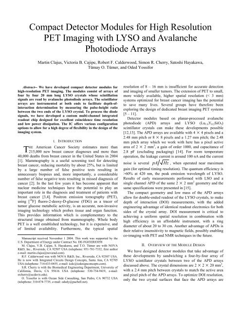
Compact Detector Modules for High Resolution<br />
PET Imaging with LYSO and Avalanche<br />
Photodiode Arrays<br />
Martin Clajus, Victoria B. Cajipe, Robert F. Calderwood, Simon R. Cherry, Satoshi Hayakawa,<br />
Tümay O. Tümer, and Oded Yossifor<br />
Abstract-- We have developed compact detector modules for<br />
high-resolution PET imaging. The modules consist of arrays of<br />
four by four 20 mm long LYSO crystals whose scintillation<br />
signals are read by avalanche photodiode arrays. The scintillator<br />
arrays are instrumented at both ends to facilitate depth-ofinteraction<br />
determination by measuring the pulse-height ratio<br />
between the two ends of the LYSO crystal. To process the diode<br />
signals, we have developed a custom multi-channel integrated<br />
readout chip designed for excellent coincidence time resolution<br />
and low power dissipation. The IC offers various configuration<br />
options to allow for a high degree of flexibility in the design of the<br />
imaging system.<br />
I. INTRODUCTION<br />
HE American Cancer Society estimates more than<br />
215,000 new breast cancer diagnoses and more than<br />
40,000 deaths from breast cancer in the United States in 2004<br />
[1]. Mammography is a useful screening tool for detecting<br />
breast cancer, reducing mortality by about 25%, but is limited<br />
by a large number of false positive tests resulting in<br />
unnecessary biopsies and, more importantly, a considerable<br />
number of false negative tests resulting in missed diagnosis of<br />
cancer [2]. In the last few years it has become apparent that<br />
nuclear medicine techniques have the potential to play an<br />
important role in the diagnosis and treatment of patients with<br />
breast cancer [3,4]. Positron emission tomography (PET),<br />
using [ 18 T<br />
F] fluoro-2-deoxy-D-glucose (FDG) as a tracer of<br />
tumor glucose metabolic activity, is an accurate, non-invasive<br />
imaging technology which probes tissue and organ function.<br />
This provides information which is complementary to the<br />
structural image obtained from mammography. Whole body<br />
PET is a well established technology, but it is expensive, and<br />
of limited availability. Furthermore, the typical spatial<br />
Manuscript received November 1 2004. This work was supported by the<br />
U.S. Department of Energy under Contract No. DE-FG03ER83058<br />
M. Clajus, V.B. Cajipe, S. Hayakawa, and T.O. Tümer are with <strong>NOVA</strong><br />
R&D, <strong>Inc</strong>., Riverside, CA 92507 USA (telephone: 951-781-7332, first author<br />
e-mail: martin.clajus@novarad.com).<br />
R.F. Calderwood was with <strong>NOVA</strong> R&D, <strong>Inc</strong>., Riverside, CA 92507 USA.<br />
He is now with Integrated Circuits Design Concepts, Santa Ana, CA 92705<br />
USA (telephone: 714-633-0455, e-mail: icdc@icdesignconcepts.com).<br />
S.R. Cherry is with the Biomedical Engineering Department, University of<br />
California, Davis, CA 95616 USA (telephone: 530-754-9419, e-mail:<br />
srcherry@ucdavis.edu).<br />
O. Yossifor is with Ocean Side Consulting, San Pedro, CA 90732 USA<br />
(telephone: 310-874-7735, e-mail: odedy@pacbell.net).<br />
resolution of 8 – 16 mm is insufficient for accurate detection<br />
and imaging of smaller tumors. The extension of PET to small,<br />
more widely available, higher spatial resolution (< 3 mm)<br />
systems optimized for breast cancer imaging has the potential<br />
to save many lives. Several groups have therefore been<br />
exploring the design of dedicated breast imaging PET systems<br />
[5 – 11].<br />
Detector modules based on planar-processed avalanche<br />
photodiode (APD) arrays and LYSO (Lu1.8Y0.2SiO5)<br />
scintillator crystals can make these developments possible<br />
[12,13]. The APD arrays are available with 4 × 4 pixels and a<br />
2.48 mm pitch or 8 × 8 pixels and a 1.27 mm pitch; the 2.48<br />
mm pitch array which we work with here has a pixel active<br />
area of 2 × 2 mm 2 , a gain of order 1000, and capacitance of<br />
2.8 pF (excluding packaging) [14]. For room temperature<br />
operation, the leakage current is around 100 nA and the current<br />
noise is several pA Hz , when operated near maximum<br />
gain (for optimal timing resolution). The quantum efficiency is<br />
>60% at 420 nm, the peak emission wavelength of LYSO.<br />
Results of early measurements performed with LSO and a<br />
single channel APD of the same 2 × 2 mm 2 geometry and the<br />
same specifications were presented in [15].<br />
The compact geometry and low mass of the APD arrays<br />
allow for double-ended readout of the LYSO crystals, to make<br />
depth of interaction (DOI) measurements, with the added<br />
engineering advantage of identical readout electronics for both<br />
sides of the crystal array. DOI measurement is critical to<br />
achieving a uniform spatial resolution in combination with<br />
high efficiency in an affordable instrument, with a ring<br />
diameter of about 20 to 30 cm. Another advantage of APDs is<br />
their relative insensitivity to magnetic fields, possibly enabling<br />
co-imaging with PET and NMR techniques in the future.<br />
II. OVERVIEW OF THE MODULE DESIGN<br />
We have designed detector modules that take advantage of<br />
these developments by sandwiching a four-by-four array of<br />
LYSO scintillator crystals between two of the APD arrays<br />
discussed above. The crystal dimensions are 2 × 2 × 20 mm 3 ,<br />
with a 2.4 mm pitch between crystals to match the active area<br />
and pixel pitch of the APD arrays. To optimize DOI resolution,<br />
only the two crystal surfaces that face the APD arrays are
polished; all other surfaces are saw-cut. The space between the<br />
crystals is filled with optical epoxy loaded with barium sulfate<br />
reflector.<br />
To read out these detector modules, we have developed a<br />
multi-channel readout IC optimized for high resolution<br />
APD/LYSO PET imaging. This chip, called FREDA (Fast<br />
Readout Electronics for Diode Arrays) has 64 channels,<br />
sufficient for instrumenting even the 8 × 8-pixel APD arrays<br />
with their finer position resolution. A high resolution PET<br />
scanner with DOI for breast cancer imaging can easily involve<br />
5,000 – 20,000 channels, making excellent coincidence timing<br />
resolution essential in order to handle high event rates without<br />
significant background due to accidental coincidences. Given<br />
this large channel count, power dissipation is also a critical<br />
parameter. Since the avalanche gain in an APD is relatively<br />
low (compared to a typical PMT), sophisticated low-noise<br />
electronics must be placed close to the APDs. This further<br />
complicates the power dissipation issue, especially since the<br />
APD gain depends sensitively on temperature.<br />
III. CHIP DESIGN DETAILS<br />
To address the requirements above, our chip design<br />
combines a high-speed, low-noise input amplifier with a<br />
constant-fraction discriminator (CFD). The CFD, especially<br />
when operated at the low thresholds permitted by the low<br />
amplifier noise, minimizes pulse-height dependent time walk<br />
and overall timing jitter that would degrade coincidence<br />
resolution. As shown in the top-level block diagram in Fig. 1,<br />
the IC provides on-chip circuitry to detect coincidences<br />
between the local discriminator outputs and the corresponding<br />
signals that are received from other chips in the system. For<br />
pulse-height measurements, each channel is equipped with<br />
shaper and peak/hold circuitry (cf. the channel block diagram<br />
in Fig. 2). The amplifier gains are digitally adjustable<br />
individually for each channel. When a coincidence trigger is<br />
generated, the peak of the shaper signal can be sampled and<br />
read out for any channel(s) the user selects. This flexibility<br />
permits DOI determination even in those cases where the<br />
smaller of the two scintillator signals involved is below or just<br />
barely above the discriminator threshold.<br />
Fig. 3 shows the coincidence circuitry of the FREDA IC.<br />
One-shot circuits convert the CFD output (hit) signals from<br />
each channel, whose width depends on the APD signal's time<br />
over threshold, into fixed-width pulses to provide coincidence<br />
windows of well-defined widths. A logical OR of these pulses<br />
is distributed to other FREDA chips in the detector system via<br />
the IC's CORR_OUT output. The hit signals from these other<br />
chips are received through the CORR_IN input and brought<br />
into coincidence with the local hit signals, which are delayed<br />
to match the propagation delay of the incoming signals. The<br />
delay and coincidence width are digitally adjustable over wide<br />
ranges, common to all channels. For test purposes, the chip<br />
provides the options of external and singles triggering.<br />
AIN1<br />
SIGNAL CHANNEL<br />
AOUT1<br />
V U UOUT1<br />
V V<br />
VOUT1<br />
TEST<br />
HIT1<br />
AINn<br />
AIN<br />
TEST<br />
HIT1<br />
. . .<br />
HITn<br />
ONE-SHOT<br />
ONE-SHOT<br />
. . .<br />
SIGNAL CHANNEL<br />
AOUTn<br />
UOUTn<br />
VOUTn<br />
HITn<br />
THRESHOLD SAMPLE/HOLD<br />
. . .<br />
READOUT LOGIC<br />
UOUTtr<br />
VOUTtr<br />
COINCIDENCE LOGIC AND<br />
SAMPLE/HOLD CONTROL<br />
Fig. 1. Top-level block diagram of the FREDA IC.<br />
INPUT<br />
AMPLIFIER<br />
THRESHOLD<br />
SHAPING AMPLIFIER<br />
DISCRIMINATOR<br />
SAMPLE/HOLD<br />
ANALOG OUT<br />
CORR_IN<br />
CORR_OUT<br />
TRIG<br />
BUF BUF<br />
V U<br />
V V<br />
LATCH<br />
HIT<br />
Fig. 2. Signal channel block diagram of the FREDA chip.<br />
. . .<br />
DELAY<br />
OR<br />
DELAY<br />
CORR_OUT<br />
CORR_IN<br />
. . .<br />
. . .<br />
TR1<br />
TRn<br />
OR<br />
V U<br />
V V<br />
Fig. 3. Coincidence circuitry of the FREDA IC<br />
TRIG<br />
UOUT<br />
VOUT<br />
TO/FROM<br />
OTHER CHIPS<br />
AOUT<br />
UOUT<br />
VOUT<br />
The chip facilitates the recording of signal timing<br />
information by providing inputs for two user-supplied periodic<br />
"timestamp" signals (VU and VV in Fig. 2 and Fig. 3). On any<br />
channel, the values of these signals are latched in sample-andhold<br />
(S/H) circuits each time that channel's CFD detects a hit;<br />
another pair of S/H circuits is latched whenever a coincidence
is detected. The timestamp values can be read out and digitized<br />
together with the pulse height signals and used to correct<br />
pulse-height dependent time walk or to tighten coincidence<br />
requirements in the offline analysis. By supplying the signals<br />
externally, the timing resolution and range can be optimized<br />
for each specific application, enhancing the versatility of the<br />
design. The channel timestamps are released automatically if<br />
the corresponding coincidence window expires before a<br />
coincidence is detected.<br />
A number of configuration options, including different<br />
shaping times, facilitate flexible system design and promise to<br />
make the IC and detector module useful for a wide range of<br />
applications, beyond breast cancer imaging. Addressing one of<br />
the important design requirements described above, all chip<br />
circuits are designed to minimize power dissipation.<br />
Fig. 4 shows the layout and pad assignments of the FREDA<br />
chip, which has been fabricated in a 0.35 µ m process. The<br />
APD signal inputs are located along the two long edges of the<br />
die, arranged in groups of eight channels that are separated by<br />
wide ground bands for improved noise isolation. Bias and<br />
control signal pads are found along the short edges of the chip,<br />
with power supply pads in the corners. Fig. 5 shows a<br />
photograph of the chip mounted in a CQFP package. First<br />
comprehensive test results for the FREDA chip and the<br />
detector module are expected early in 2005.<br />
Fig. 4. Layout and pad assignments of the FREDA IC.<br />
Fig. 5. Photograph of the FREDA chip mounted in a CQFP package<br />
IV. ACKNOWLEDGMENTS<br />
We are grateful to Gerard Visser, Kanai Shah, and Richard<br />
Farrell for helpful discussions about the chip design<br />
requirements.<br />
[1]<br />
V. REFERENCES<br />
American Cancer Society: Cancer Facts and Figures 2004; available at<br />
http://www.cancer. org/docroot/STT/stt_0.asp.<br />
[2] I. Andersson et al., Mammographic screening and mortality from breast<br />
cancer: The Malmö mammographic screening trial. Br. Med Journal 297,<br />
943 (1988).<br />
[3] L.P. Adler, J.P. Crowe, N.K. Al-Kaisi, and J.L. Sunshine, Evaluation of<br />
breast masses and axillary lymph nodes with [F-18] 2-deoxy-2-fluoro-Dglucose<br />
PET. Radiology 187, 743 (1993).<br />
[4] J.A. Glasby, R.A. Hawkins, C.K. Hoh, and M.E. Phelps, Use of positron<br />
emission tomography in oncology. Oncology 7, 41 (1993).<br />
[5] R.R. Raylman, S. Majewski, R. Wojcik, A.G. Weisenberger, B. Kross,<br />
V. Popov, and H. Bishop. The potential role of positron emission<br />
mammography for detection of breast cancer. A phantom study. Med.<br />
Physics 27, 1943 (2000).<br />
[6] C. J. Thompson et al., Positron Emission Mammography (PEM): A<br />
Promising Technique for Detecting Breast Cancer. IEEE Trans. Nucl.<br />
Sci., 42, 1012 (1995).<br />
[7] I. Weinberg et al., Preliminary Results for Positron Emission<br />
Mammography: Real-time Functional Breast Imaging in a Conventional<br />
Mammography Gantry. Eur. Journal of Nuclear Medicine, 23, 804<br />
(1996).<br />
[8] R. Freifelder and J. Karp, Dedicated PET Scanners for Breast Imaging.<br />
Physics in Medicine and Biology, 42, 2463(1997).<br />
[9] G. Hutchins and A. Simon, Evaluation of Prototype Geometries for<br />
Breast Imaging with PET Radiopharmaceuticals. Journal of Nuclear<br />
Medicine, 36, 69P (1995).<br />
[10] W.W. Moses, T.F. Budinger, R.H. Huesman, and S.E. Derenzo, PET<br />
Camera Designs for Imaging Breast Cancer and Axillary Node<br />
Involvement. Journal of Nuclear Medicine, 36, 69P (1995).<br />
[11] N.K. Doshi, Y. Shao, R.W. Silverman, S.R. Cherry, Design and<br />
Evaluation of an LSO PET Detector for Breast Cancer Imaging. Medical<br />
Physics, 27, 1535 (2000).<br />
[12] K.S. Shah, R. Farrell, R.F. Grazioso et al., Planar processed APDs and<br />
APD arrays for scintillation detection. IEEE MIC conf. record, Seattle,<br />
1999.<br />
[13] Y. Shao et al., Design studies of a high-resolution PET detector using<br />
APD arrays. IEEE Trans. Nucl. Sci. 42, 1051(2000).<br />
[14] RMD, <strong>Inc</strong>., Watertown, MA, Silicon Avalanche Photodiodes:<br />
Specifications [Online]. http://www.rmdinc.com/production/apd.html.<br />
[15] G. Visser, S. Cherry, M. Clajus, Y. Shao, and T.O. Tümer, Development<br />
of low power high speed readout electronics for high resolution PET<br />
imaging with LSO and avalanche photodiode arrays, IEEE MIC<br />
conference record, San Diego, 2001.