A Prototype Implementation of the TinyOS Hardware Abstraction ...
A Prototype Implementation of the TinyOS Hardware Abstraction ...
A Prototype Implementation of the TinyOS Hardware Abstraction ...
You also want an ePaper? Increase the reach of your titles
YUMPU automatically turns print PDFs into web optimized ePapers that Google loves.
A <strong>Prototype</strong> <strong>Implementation</strong> <strong>of</strong> <strong>the</strong> <strong>TinyOS</strong> <strong>Hardware</strong><br />
<strong>Abstraction</strong> Architecture for Ferroelectric RAM<br />
Abstract—This report presents a hardware driver for <strong>the</strong> Ramtron<br />
Ferroelectric RAM (FRAM, FeRAM) chips for use in <strong>TinyOS</strong><br />
according to <strong>TinyOS</strong>' <strong>Hardware</strong> <strong>Abstraction</strong> Architecture.<br />
FRAM is a replacement for flash memory, suitable for usage in<br />
Wireless Sensor Networks (WSNs) for its properties. The properties<br />
<strong>of</strong> FRAM and flash are shortly depicted and compared. The<br />
design <strong>of</strong> <strong>the</strong> driver implementation is described, including a chip<br />
clustering method to circumvent <strong>the</strong> capacity limitation. The<br />
driver <strong>of</strong>fers <strong>the</strong> DirectStorage interface and <strong>the</strong> BlockStorage<br />
interface for usage by applications. Comments on <strong>the</strong> suitability<br />
<strong>of</strong> <strong>the</strong> provided interfaces, intended for flash memory originally,<br />
for FRAM are given.<br />
Index Terms—<strong>TinyOS</strong>, FRAM, driver, hardware abstraction<br />
architecture<br />
I. INTRODUCTION<br />
In this report, <strong>TinyOS</strong>, <strong>TinyOS</strong> drivers and FRAM are introduced<br />
shortly. Then, <strong>the</strong> architecture <strong>of</strong> <strong>the</strong> driver implementation<br />
is shown, <strong>the</strong> clustering <strong>of</strong> several chips is described<br />
and finally <strong>the</strong> suitability <strong>of</strong> existing <strong>TinyOS</strong> flash storage<br />
abstractions is assessed.<br />
A. <strong>TinyOS</strong> and its Driver Model<br />
<strong>TinyOS</strong> is an operating system and library <strong>of</strong> code components<br />
for sensor networks. The fur<strong>the</strong>r development is done by<br />
working groups and by user contributions. Working groups can<br />
issue <strong>TinyOS</strong> Extension Proposals (TEPs), specifying best<br />
practices for new code contributions.<br />
TEP2 [1] is one <strong>of</strong> <strong>the</strong> central TEPs for <strong>TinyOS</strong> 2.0. It describes<br />
a hardware abstraction architecture (HAA). The HAA<br />
specifies a three-layered architecture for driver implementations.<br />
The three layers comprise <strong>the</strong> hardware presentation<br />
layer (HPL), which exposes <strong>the</strong> hardware's capabilities directly,<br />
<strong>the</strong> hardware adaptation layer (HAL) which abstracts <strong>the</strong><br />
hardware and allows to maintain states in s<strong>of</strong>tware, and <strong>the</strong><br />
hardware interface layer (HIL) which <strong>of</strong>fers a standardized<br />
platform-independent interface for applications, irrespective <strong>of</strong><br />
<strong>the</strong> underlying hardware components. Drivers reside in a chip<br />
directory by convention, with some additional code in a platform<br />
directory where code is placed which states <strong>the</strong> platform<br />
specifics, like specific hardware pins.<br />
B. Ferroelectric RAM (FRAM)<br />
FRAM is a relatively new memory technology which combines<br />
<strong>the</strong> best from static RAM memory (fast, energy efficient)<br />
This work was funded by <strong>the</strong> 7 th Framework Programme <strong>of</strong> <strong>the</strong> European<br />
Commission.<br />
Sebastian A. Bachmaier<br />
Material Testing Institute<br />
Universität Stuttgart<br />
Stuttgart, Germany<br />
sebastian.bachmaier@mpa.uni-stuttgart.de<br />
39<br />
and flash memory (non-volatile). It is based on a ferroelectric<br />
material which retains its state even when currentless. FRAM<br />
is a suitable replacement for flash.<br />
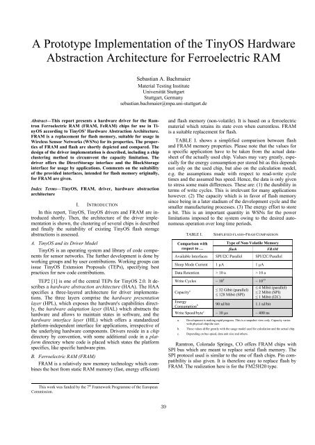
TABLE I. shows a simplified comparison between flash<br />
and FRAM memory properties. Please note that <strong>the</strong> values for<br />
a specific application have to be taken from <strong>the</strong> actual datasheet<br />
<strong>of</strong> <strong>the</strong> actually used chip. Values may vary greatly, especially<br />
for <strong>the</strong> energy consumption per stored bit as this depends<br />
not only on <strong>the</strong> used chip, but also on <strong>the</strong> calculation model,<br />
e.g. <strong>the</strong> assumptions made with respect to read-write cycle<br />
times and <strong>the</strong> assumed bus speed. Hence, <strong>the</strong> data is only given<br />
to stress some main differences. These are: (1) <strong>the</strong> durability in<br />
terms <strong>of</strong> write cycles. This is irrelevant for many applications<br />
however. (2) The capacity which is in favor <strong>of</strong> flash memory<br />
since being in a later stadium <strong>of</strong> <strong>the</strong> development cycle and <strong>the</strong><br />
smaller manufacturing processes. (3) The energy effort to store<br />
a bit. This is an important quantity in WSNs for <strong>the</strong> power<br />
limitations imposed to <strong>the</strong> system owing to <strong>the</strong> desired autonomous<br />
operation over long time periods.<br />
TABLE I. SIMPLIFIED FLASH–FRAM COMPARISON<br />
Comparison with<br />
respect to …<br />
Type <strong>of</strong> Non-Volatile Memory<br />
flash FRAM<br />
Available Interfaces SPI/I2C/Parallel SPI/I2C/Parallel<br />
Sleep Mode Current 1 µA 1 µA<br />
Data Retention > 10 a > 10 a<br />
Write Cycles ~ 10 5 ~ 10 10<br />
Capacity a<br />
Energy<br />
Consumption b<br />
≤ 32 Gibit (parallel)<br />
≤ 128 Mibit (SPI)<br />
≤ 4 Mibit (parallel)<br />
≤ 2 Mibit (SPI)<br />
≤ 1 Mibit (I2C)<br />
90 nJ/bit 1.1 nJ/bit<br />
Write Speed/byte c ~ 10 µs ~ 400 ns<br />
a. Development is making rapid progress. This is a snapshot view only. Capacity varies<br />
with physical chip/die size.<br />
b. These values differ greatly with <strong>the</strong> usage model used for calculation and <strong>the</strong> actual chip.<br />
c. Depending on bus speed, data unit size and o<strong>the</strong>rs.<br />
Ramtron, Colorado Springs, CO <strong>of</strong>fers FRAM chips with<br />
SPI bus which are meant to replace serial flash memory. The<br />
SPI protocol used is similar to <strong>the</strong> one <strong>of</strong> flash chips. Pin compatibility<br />
is also given. It is <strong>the</strong>refore easy to replace flash by<br />
FRAM. The realization here is for <strong>the</strong> FM25H20 type.
II. IMPLEMENTATION<br />
The implementation follows that <strong>of</strong> <strong>the</strong> STM25P flash chip<br />
by Hui [2]. The components should reside in tinyos-<br />
2.x/tos/chips/fm25h and platform//chips/fm25h.<br />
However, <strong>the</strong> contribution resides at tinyos-2.x-contrib/ustutt<br />
where it can be retrieved from.<br />
A. <strong>Hardware</strong> Presentation Layer (HPL)<br />
The HPL <strong>of</strong>fers no erase and pageProgram commands, but<br />
<strong>of</strong>fers a write command instead. In FRAM writes are possible<br />
without prior erase. The write command operates on data units<br />
<strong>of</strong> down to single bytes. Flush is not implemented since data is<br />
always written through. Sleep mode support is available.<br />
B. <strong>Hardware</strong> Adaptation Layer (HAL)<br />
Two HAL implementations<br />
are <strong>of</strong>fered: one simpler<br />
HAL for single chip<br />
mode and a ClusterHAL<br />
component for clustered<br />
operation <strong>of</strong> several chips<br />
under a flat, continuous<br />
address space. Standard<br />
wiring uses <strong>the</strong> single chip<br />
HAL. The single chip HAL<br />
is similar to <strong>the</strong> STM25P<br />
implementation.<br />
C. ClusterHAL<br />
While <strong>the</strong> FRAM <strong>of</strong>fers<br />
some advantages over flash<br />
memory it still <strong>of</strong>fers less<br />
capacity. This is due to <strong>the</strong><br />
smaller packing density,<br />
which is caused by <strong>the</strong> larger<br />
manufacturing process sizes<br />
and <strong>the</strong> ferroelectric material<br />
properties.<br />
We <strong>the</strong>refore had to bundle<br />
several chips to get a<br />
memory size comparable to<br />
<strong>the</strong> 1 MiB <strong>of</strong> <strong>the</strong> TelosB<br />
Figure 1. HAA <strong>of</strong> <strong>the</strong> clustered operation:<br />
<strong>the</strong> HPL is ignorant <strong>of</strong> <strong>the</strong> actually<br />
used chip as this is dispatched by<br />
<strong>the</strong> HAL (GeneralIO interface)<br />
which were used as reference. The resulting cluster was desired<br />
to act like one big memory under a unified address space. This<br />
means a dispatcher has to handle accesses to <strong>the</strong> unified address<br />
space and direct <strong>the</strong>m to <strong>the</strong> corresponding chip. The<br />
dispatcher is provided on <strong>the</strong> HAL layer. This has <strong>the</strong> advantage<br />
<strong>of</strong> having <strong>the</strong> HPL unchanged for cluster or single chip<br />
operation. Fur<strong>the</strong>rmore, HPL can be stateless and "present" just<br />
<strong>the</strong> operations <strong>the</strong> FRAM <strong>of</strong>fers. However, <strong>the</strong> layering in this<br />
approach is not strictly adhered to as for clustered operation <strong>the</strong><br />
IO pins are handled by <strong>the</strong> HAL, transparently to <strong>the</strong> HPL (see<br />
Figure 1). The HPL just accesses <strong>the</strong> chip select (CS) to activate<br />
<strong>the</strong> large virtual chip (<strong>of</strong> which <strong>the</strong> HPL is ignorant <strong>of</strong>)<br />
and <strong>the</strong> HAL activates <strong>the</strong> appropriate physical chip determined<br />
by <strong>the</strong> memory address that is accessed. Memory accesses<br />
across chips are split into several separate operations.<br />
O<strong>the</strong>r approaches are conceivable and can be implemented<br />
later. E.g., a strictly layered architecture would access several<br />
individual HPLs, but code is replicated <strong>the</strong>n.<br />
40<br />
D. <strong>Hardware</strong> Interface Layer (HIL)<br />
For a description <strong>of</strong> two prototype implementations <strong>of</strong> HIL<br />
refer to chapter III. The implementation here follows <strong>the</strong><br />
STM25P implementation.<br />
III. SUITABILTY ASSESMENT OF FLASH ABSTRACTIONS<br />
A. BlockStorage Interface (TEP103)<br />
TEP103 [3] standardizes three fundamental storage abstractions<br />
found in typical sensor network applications: BlockStorage<br />
for program memory, ConfigStorage for little chunks <strong>of</strong><br />
configuration data and LogStorage for data logging application.<br />
TEP103 aims solely at flash memory and incorporates specialties<br />
<strong>of</strong> flash memory. However, <strong>the</strong> flash functionality is a<br />
subset <strong>of</strong> FRAM functionality, i.e. FRAM has fewer restrictions<br />
to consider. It should <strong>the</strong>refore be possible to realize <strong>the</strong>se<br />
storage abstractions for FRAM. For workload restriction, <strong>of</strong> <strong>the</strong><br />
three storage abstraction <strong>of</strong> TEP103, only <strong>the</strong> BlockStorage<br />
was implemented exemplarily.<br />
B. DirectStorage Interface (TEP128)<br />
TEP 128 ([4], draft version) describes an interface for direct<br />
access to non-volatile storage. It <strong>of</strong>fers read, write, erase, flush<br />
and crc commands. It differs primarily in two points from <strong>the</strong><br />
abstractions <strong>of</strong> TEP103: (1) <strong>the</strong> interface is an application indifferent<br />
general purpose interface, and (2) <strong>the</strong> implementation<br />
(in conjunction with <strong>the</strong> VolumeSettings interface) is platform<br />
independent. TEP 129 describes a new set <strong>of</strong> BlockStorage,<br />
ConfigStorage and LogStorage which resides above <strong>the</strong> platform-independent<br />
intermediate DirectStorage interface.<br />
There are some comments to <strong>the</strong> DirectStorage interface<br />
which occurred during implementation <strong>of</strong> <strong>the</strong> interface. Due to<br />
<strong>the</strong> missing sector size <strong>of</strong> FRAM, <strong>the</strong> sector size can artificially<br />
be set to ei<strong>the</strong>r an arbitrary size (for easier programming a<br />
fraction <strong>of</strong> a power <strong>of</strong> two) or it can be set to 1 which is <strong>the</strong><br />
natural sector size <strong>of</strong> FRAM. This leads to two consequences:<br />
(1) <strong>the</strong> volume information structure fm25h_volume_info_t<br />
which is set in <strong>the</strong> tool tos-storage-fm25h should define both<br />
base and size as uint32_t instead <strong>of</strong> unit8_t to accommodate <strong>the</strong><br />
larger size numbers (this is internal to <strong>the</strong> chip specific tool<br />
chain and has no consequences to <strong>the</strong> interfaces), and (2) <strong>the</strong><br />
erase command's parameter eraseUnitIndex (and <strong>the</strong> corresponding<br />
eraseDone event's) should likewise be uint32_t, instead<br />
<strong>of</strong> uint16_t. This results from <strong>the</strong> erase unit size which is<br />
<strong>of</strong> size 1 as well. However, here <strong>the</strong> advantage <strong>of</strong> an artificially<br />
introduced larger erase unit size becomes obvious. For erasing<br />
larger memory regions less function calls were necessary <strong>the</strong>n.<br />
A last comment is given on <strong>the</strong> DirectModify interface signature.<br />
It is perhaps preferable to name all completion events in<br />
<strong>the</strong> same manner and so rename <strong>the</strong> completion event <strong>of</strong> modify(…)<br />
to modifyDone(…).<br />
IV. CONCLUSION<br />
FRAM can replace flash memory when low-power operation<br />
in combination with short write access times is <strong>of</strong> importance.<br />
Drawback is <strong>the</strong> smaller maximum capacity per chip. If<br />
<strong>the</strong> capacity is a limiting factor, several chips can be clustered<br />
as proposed. Several HIL interfaces originally intended for<br />
flash memory were successfully implemented. Recommenda-
tions were made to <strong>the</strong> DirectStorage and DirectModify interfaces,<br />
both being still in draft status and open for changes.<br />
ACKNOWLEDGMENT<br />
S. B. likes to thank Helmut Ernst for his support in <strong>the</strong><br />
hardware development <strong>of</strong> <strong>the</strong> sensor nodes used for this work.<br />
[1]<br />
REFERENCES<br />
V. Handziski, J. Polastre, J.-H. Hauer, C. Sharp, A. Wolisz, D. Culler,<br />
D. Gay, "TEP2 – <strong>Hardware</strong> <strong>Abstraction</strong> Architecture".<br />
41<br />
http://www.tinyos.net/tinyos-2.x/doc/html/tep2.html. Date <strong>of</strong> access:<br />
2009-05-25<br />
[2] J. Hui, "<strong>Implementation</strong> <strong>of</strong> <strong>the</strong> TEP103 for <strong>the</strong> ST M25P serial code<br />
flash". http://tinyos.cvs.sourceforge.net/viewvc/tinyos/tinyos-<br />
2.x/tos/chips/ stm25p. Date <strong>of</strong> access: 2009-05-28<br />
[3] D. Gay, J. Hui, "TEP103 – Permanent Data Storage (flash)".<br />
http://www.tinyos.net/tinyos-2.x/doc/html/tep103.html. Date <strong>of</strong> access:<br />
2009-05-25<br />
[4] D. Moss, J. Du, P. Dutta, D. Ganesan, K. Klues, A. Martin, G. Mathur,<br />
"TEP128 - Platform Independent Non-Volatile Storage <strong>Abstraction</strong>s".<br />
http://www.tinyos.net/tinyos-2.1.0/doc/html/tep128.html. Date <strong>of</strong> access:<br />
2009-05-25


