- Page 1 and 2:
OP AMP APPLICATIONS Walter G. Jung
- Page 3:
OP AMP APPLICATIONS H Op Amp Histor
- Page 6 and 7:
OP AMP APPLICATIONS
- Page 8 and 9:
H.2 OP AMP APPLICATIONS A final maj
- Page 10 and 11:
H.4 OP AMP APPLICATIONS Black's Fee
- Page 12 and 13:
H.6 OP AMP APPLICATIONS REFERENCES:
- Page 14 and 15:
H.8 OP AMP APPLICATIONS NOTES:
- Page 16 and 17:
OP AMP APPLICATIONS Otto Schmitt di
- Page 18 and 19:
OP AMP APPLICATIONS Fig. 10a of Ref
- Page 20 and 21:
OP AMP APPLICATIONS Karl Swartzel's
- Page 22 and 23:
OP AMP APPLICATIONS Naming the Op A
- Page 24 and 25:
OP AMP APPLICATIONS amplifier secon
- Page 26 and 27:
OP AMP APPLICATIONS Despite that, o
- Page 28 and 29:
OP AMP APPLICATIONS The Twilight Ye
- Page 30 and 31:
OP AMP APPLICATIONS 13. Franklin Of
- Page 32 and 33:
OP AMP APPLICATIONS 39. David A. Mi
- Page 34 and 35:
OP AMP APPLICATIONS H.28 NOTES:
- Page 36 and 37:
OP AMP APPLICATIONS The nucleus of
- Page 38 and 39:
OP AMP APPLICATIONS The second P65
- Page 40 and 41:
OP AMP APPLICATIONS Figure H-10 bel
- Page 42 and 43:
OP AMP APPLICATIONS The Many Op Amp
- Page 44 and 45:
OP AMP APPLICATIONS Model 45, 44 an
- Page 46 and 47:
OP AMP APPLICATIONS The model 50 an
- Page 48 and 49:
OP AMP APPLICATIONS 15. Dan Sheingo
- Page 50 and 51:
OP AMP APPLICATIONS H.44 NOTES:
- Page 52 and 53:
OP AMP APPLICATIONS Many design pri
- Page 54 and 55:
OP AMP APPLICATIONS connected betwe
- Page 56 and 57:
OP AMP APPLICATIONS The AD741— a
- Page 58 and 59:
OP AMP APPLICATIONS In late 1969, B
- Page 60 and 61:
OP AMP APPLICATIONS The OP97 best g
- Page 62 and 63:
OP AMP APPLICATIONS Another key poi
- Page 64 and 65:
OP AMP APPLICATIONS The OP27 and OP
- Page 66 and 67:
OP AMP APPLICATIONS Precision JFET
- Page 68 and 69:
OP AMP APPLICATIONS various power r
- Page 70 and 71:
OP AMP APPLICATIONS Released in 198
- Page 72 and 73:
OP AMP APPLICATIONS High Speed IC O
- Page 74 and 75:
OP AMP APPLICATIONS 15. Modesto Mai
- Page 76 and 77:
OP AMP APPLICATIONS 50. JoAnn Close
- Page 78 and 79:
OP AMP APPLICATIONS H.72 Classic Ca
- Page 80 and 81:
OP AMP APPLICATIONS
- Page 82 and 83:
1.2 OP AMP APPLICATIONS
- Page 84 and 85:
1.4 OP AMP APPLICATIONS talk in ide
- Page 86 and 87:
1.6 OP AMP APPLICATIONS Standard Op
- Page 88 and 89:
1.8 OP AMP APPLICATIONS The Inverti
- Page 90 and 91:
OP AMP APPLICATIONS For an ideal op
- Page 92 and 93:
OP AMP APPLICATIONS It is useful to
- Page 94 and 95:
OP AMP APPLICATIONS to normal divis
- Page 96 and 97:
OP AMP APPLICATIONS rail, -VS. We w
- Page 98 and 99:
OP AMP APPLICATIONS More recently,
- Page 100 and 101:
OP AMP APPLICATIONS REFERENCES: INT
- Page 102 and 103:
OP AMP APPLICATIONS 1.22 NOTES:
- Page 104 and 105:
OP AMP APPLICATIONS Current Feedbac
- Page 106 and 107:
OP AMP APPLICATIONS Current Feedbac
- Page 108 and 109:
OP AMP APPLICATIONS When transistor
- Page 110 and 111:
OP AMP APPLICATIONS 1.30 NOTES:
- Page 112 and 113:
OP AMP APPLICATIONS OP113/213/413 f
- Page 114 and 115:
OP AMP APPLICATIONS Op Amp Input St
- Page 116 and 117:
OP AMP APPLICATIONS Bias Current Co
- Page 118 and 119:
OP AMP APPLICATIONS Bias Current Co
- Page 120 and 121:
OP AMP APPLICATIONS Rail-Rail Input
- Page 122 and 123:
OP AMP APPLICATIONS switched off at
- Page 124 and 125:
OP AMP APPLICATIONS Output Stages T
- Page 126 and 127:
OP AMP APPLICATIONS Op amps built o
- Page 128 and 129:
OP AMP APPLICATIONS At this point i
- Page 130 and 131:
OP AMP APPLICATIONS Op Amp Process
- Page 132 and 133:
OP AMP APPLICATIONS 1.52 NOTES:
- Page 134 and 135:
OP AMP APPLICATIONS Chopper stabili
- Page 136 and 137:
OP AMP APPLICATIONS Offset Adjustme
- Page 138 and 139:
OP AMP APPLICATIONS Input Offset Vo
- Page 140 and 141:
OP AMP APPLICATIONS Extremely low i
- Page 142 and 143:
OP AMP APPLICATIONS Input Impedance
- Page 144 and 145:
OP AMP APPLICATIONS Open-Loop Gain
- Page 146 and 147:
OP AMP APPLICATIONS An oscilloscope
- Page 148 and 149:
OP AMP APPLICATIONS Op Amp Frequenc
- Page 150 and 151:
OP AMP APPLICATIONS depend on the p
- Page 152 and 153:
OP AMP APPLICATIONS approximately -
- Page 154 and 155:
OP AMP APPLICATIONS The Bode plot o
- Page 156 and 157:
OP AMP APPLICATIONS Operational Amp
- Page 158 and 159:
OP AMP APPLICATIONS Consider for ex
- Page 160 and 161:
OP AMP APPLICATIONS The general equ
- Page 162 and 163:
OP AMP APPLICATIONS density on the
- Page 164 and 165:
OP AMP APPLICATIONS leave bandwidth
- Page 166 and 167:
OP AMP APPLICATIONS A DC signal app
- Page 168 and 169:
OP AMP APPLICATIONS Op Amp Distorti
- Page 170 and 171:
OP AMP APPLICATIONS Common-mode rej
- Page 172 and 173:
OP AMP APPLICATIONS Power Supplies
- Page 174 and 175:
OP AMP APPLICATIONS 1.94 NOTES:
- Page 176 and 177:
OP AMP APPLICATIONS The challenge o
- Page 178 and 179:
OP AMP APPLICATIONS Chopper Stabili
- Page 180 and 181:
OP AMP APPLICATIONS A comparison be
- Page 182 and 183:
OP AMP APPLICATIONS REFERENCES: PRE
- Page 184 and 185:
OP AMP APPLICATIONS The next comple
- Page 186 and 187:
OP AMP APPLICATIONS Figure 1-98 bel
- Page 188 and 189:
OP AMP APPLICATIONS where A is the
- Page 190 and 191:
OP AMP APPLICATIONS dominant pole c
- Page 192 and 193:
OP AMP APPLICATIONS At the dynamic
- Page 194 and 195:
OP AMP APPLICATIONS Now, consider a
- Page 196 and 197:
OP AMP APPLICATIONS The AD8011 CFB
- Page 198 and 199:
OP AMP APPLICATIONS Effects of Feed
- Page 200 and 201:
OP AMP APPLICATIONS On the other ha
- Page 202 and 203:
OP AMP APPLICATIONS A similar analy
- Page 204 and 205:
OP AMP APPLICATIONS A CFB op amp, o
- Page 206 and 207:
OP AMP APPLICATIONS CFB op amps gen
- Page 208 and 209:
OP AMP APPLICATIONS 1.128 NOTES:
- Page 210 and 211:
OP AMP APPLICATIONS
- Page 212 and 213:
2.2 OP AMP APPLICATIONS In-Amp Defi
- Page 214 and 215:
2.4 OP AMP APPLICATIONS In general,
- Page 216 and 217:
2.6 OP AMP APPLICATIONS David Birt
- Page 218 and 219:
2.8 OP AMP APPLICATIONS IC in-amps
- Page 220 and 221:
2.10 OP AMP APPLICATIONS The AD627
- Page 222 and 223:
2.12 OP AMP APPLICATIONS As a resul
- Page 224 and 225:
2.14 OP AMP APPLICATIONS Under thes
- Page 226 and 227:
2.16 OP AMP APPLICATIONS The AD623
- Page 228 and 229:
2.18 OP AMP APPLICATIONS The total
- Page 230 and 231:
2.20 OP AMP APPLICATIONS Now that a
- Page 232 and 233:
2.22 OP AMP APPLICATIONS In-Amp Bri
- Page 234 and 235:
2.24 OP AMP APPLICATIONS In-Amp Inp
- Page 236 and 237:
2.26 OP AMP APPLICATIONS In-Amp A/D
- Page 238 and 239:
2.28 OP AMP APPLICATIONS In-Amp Rem
- Page 240 and 241:
2.30 OP AMP APPLICATIONS Classic Ca
- Page 242 and 243:
2.32 OP AMP APPLICATIONS A PGA is u
- Page 244 and 245:
OP AMP APPLICATIONS PGA Application
- Page 246 and 247:
2.36 OP AMP APPLICATIONS In practic
- Page 248 and 249:
2.38 OP AMP APPLICATIONS Differenti
- Page 250 and 251:
2.40 OP AMP APPLICATIONS switches.
- Page 252 and 253:
2.42 OP AMP APPLICATIONS NOTES:
- Page 254 and 255:
2.44 OP AMP APPLICATIONS Transforme
- Page 256 and 257:
2.46 OP AMP APPLICATIONS Motor Cont
- Page 258 and 259:
2.48 OP AMP APPLICATIONS Digital Is
- Page 260 and 261:
2.50 OP AMP APPLICATIONS The power
- Page 262 and 263:
2.52 OP AMP APPLICATIONS NOTES:
- Page 264 and 265:
OP AMP APPLICATIONS
- Page 266 and 267:
3.2 OP AMP APPLICATIONS Another key
- Page 268 and 269:
3.4 OP AMP APPLICATIONS It is highl
- Page 270 and 271:
3.6 OP AMP APPLICATIONS NOTES:
- Page 272 and 273:
3.8 OP AMP APPLICATIONS The first a
- Page 274 and 275:
3.10 OP AMP APPLICATIONS but if the
- Page 276 and 277:
3.12 OP AMP APPLICATIONS Calculatin
- Page 278 and 279:
3.14 OP AMP APPLICATIONS Quantifyin
- Page 280 and 281:
3.16 OP AMP APPLICATIONS Many curre
- Page 282 and 283:
3.18 OP AMP APPLICATIONS Total harm
- Page 284 and 285:
3.20 OP AMP APPLICATIONS REFERENCES
- Page 286 and 287:
3.22 OP AMP APPLICATIONS Although t
- Page 288 and 289:
3.24 OP AMP APPLICATIONS On the oth
- Page 290 and 291:
3.26 OP AMP APPLICATIONS Op Amp Con
- Page 292 and 293:
3.28 OP AMP APPLICATIONS Within the
- Page 294 and 295:
3.30 OP AMP APPLICATIONS Driving CM
- Page 296 and 297:
3.32 OP AMP APPLICATIONS circuit sh
- Page 298 and 299:
3.34 OP AMP APPLICATIONS A DC coupl
- Page 300 and 301:
3.36 OP AMP APPLICATIONS Transforme
- Page 302 and 303:
3.38 OP AMP APPLICATIONS A block di
- Page 304 and 305:
3.40 OP AMP APPLICATIONS Overvoltag
- Page 306 and 307:
3.42 OP AMP APPLICATIONS NOTES:
- Page 308 and 309:
3.44 OP AMP APPLICATIONS Note that
- Page 310 and 311:
3.46 OP AMP APPLICATIONS REFERENCES
- Page 312 and 313:
3.48 OP AMP APPLICATIONS Differenti
- Page 314 and 315: 3.50 OP AMP APPLICATIONS A modified
- Page 316 and 317: 3.52 OP AMP APPLICATIONS An Active
- Page 318 and 319: 3.54 OP AMP APPLICATIONS NOTES:
- Page 320 and 321: OP AMP APPLICATIONS
- Page 322 and 323: 4.2 OP AMP APPLICATIONS seem equall
- Page 324 and 325: 4.4 OP AMP APPLICATIONS A quite com
- Page 326 and 327: 4.6 OP AMP APPLICATIONS NOTES:
- Page 328 and 329: 4.8 OP AMP APPLICATIONS Strain gage
- Page 330 and 331: OP AMP APPLICATIONS In each case, t
- Page 332 and 333: 4.12 OP AMP APPLICATIONS In summary
- Page 334 and 335: 4.14 OP AMP APPLICATIONS A much bet
- Page 336 and 337: 4.16 OP AMP APPLICATIONS Another ci
- Page 338 and 339: 4.18 OP AMP APPLICATIONS Driving Re
- Page 340 and 341: 4.20 OP AMP APPLICATIONS For this r
- Page 342 and 343: 4.22 OP AMP APPLICATIONS System off
- Page 344 and 345: 4.24 OP AMP APPLICATIONS A very pow
- Page 346 and 347: 4.26 OP AMP APPLICATIONS NOTES:
- Page 348 and 349: 4.28 OP AMP APPLICATIONS From equat
- Page 350 and 351: 4.30 OP AMP APPLICATIONS Instrument
- Page 352 and 353: 4.32 OP AMP APPLICATIONS Pressures
- Page 354 and 355: 4.34 OP AMP APPLICATIONS Another ex
- Page 356 and 357: 4.36 OP AMP APPLICATIONS until the
- Page 358 and 359: 4.38 OP AMP APPLICATIONS NOTES:
- Page 360 and 361: 4.40 OP AMP APPLICATIONS The equiva
- Page 362 and 363: 4.42 OP AMP APPLICATIONS For exampl
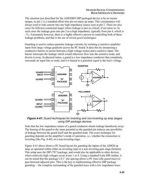
- Page 366 and 367: 4.46 OP AMP APPLICATIONS In the inv
- Page 368 and 369: 4.48 OP AMP APPLICATIONS is then al
- Page 370 and 371: 4.50 OP AMP APPLICATIONS Preamplifi
- Page 372 and 373: 4.52 OP AMP APPLICATIONS Photodiode
- Page 374 and 375: 4.54 OP AMP APPLICATIONS spectral d
- Page 376 and 377: 4.56 OP AMP APPLICATIONS Summary of
- Page 378 and 379: 4.58 OP AMP APPLICATIONS Since f2 i
- Page 380 and 381: 4.60 OP AMP APPLICATIONS The availa
- Page 382 and 383: 4.62 OP AMP APPLICATIONS frequency
- Page 384 and 385: 4.64 OP AMP APPLICATIONS To maximiz
- Page 386 and 387: 4.66 OP AMP APPLICATIONS down to lo
- Page 388 and 389: 4.68 OP AMP APPLICATIONS NOTES:
- Page 390 and 391: 4.70 OP AMP APPLICATIONS Resistance
- Page 392 and 393: 4.72 OP AMP APPLICATIONS Figure 4-6
- Page 394 and 395: 4.74 OP AMP APPLICATIONS Since ever
- Page 396 and 397: 4.76 OP AMP APPLICATIONS Type K the
- Page 398 and 399: 4.78 OP AMP APPLICATIONS Although t
- Page 400 and 401: 4.80 OP AMP APPLICATIONS To elimina
- Page 402 and 403: 4.82 OP AMP APPLICATIONS The thermi
- Page 404 and 405: 4.84 OP AMP APPLICATIONS Semiconduc
- Page 406 and 407: 4.86 OP AMP APPLICATIONS The voltag
- Page 408 and 409: 4.88 OP AMP APPLICATIONS For a grea
- Page 410 and 411: 4.90 OP AMP APPLICATIONS The net co
- Page 412 and 413: 4.92 OP AMP APPLICATIONS Classic Ca
- Page 414 and 415:
OP AMP APPLICATIONS
- Page 416 and 417:
5.2 OP AMP APPLICATIONS An ideal fi
- Page 418 and 419:
5.4 OP AMP APPLICATIONS NOTES:
- Page 420 and 421:
5.6 OP AMP APPLICATIONS ~ Figure 5-
- Page 422 and 423:
5.8 OP AMP APPLICATIONS Rewriting t
- Page 424 and 425:
5.10 OP AMP APPLICATIONS MAGNITUDE
- Page 426 and 427:
5.12 OP AMP APPLICATIONS Allpass Fi
- Page 428 and 429:
5.14 OP AMP APPLICATIONS Phase Resp
- Page 430 and 431:
5.16 OP AMP APPLICATIONS It is also
- Page 432 and 433:
5.18 OP AMP APPLICATIONS If the tim
- Page 434 and 435:
5.20 OP AMP APPLICATIONS because th
- Page 436 and 437:
5.22 OP AMP APPLICATIONS Linear Pha
- Page 438 and 439:
5.24 OP AMP APPLICATIONS Since the
- Page 440 and 441:
5.26 OP AMP APPLICATIONS Using the
- Page 442 and 443:
5.28 OP AMP APPLICATIONS AMPLITUDE
- Page 444 and 445:
AMPLITUDE (dB) 5.30 OP AMP APPLICAT
- Page 446 and 447:
AMPLITUDE (V) AMPLITUDE (dB) 5.32 O
- Page 448 and 449:
AMPLITUDE (dB) 5.34 OP AMP APPLICAT
- Page 450 and 451:
5.36 OP AMP APPLICATIONS AMPLITUDE
- Page 452 and 453:
AMPLITUDE (dB) 5.38 OP AMP APPLICAT
- Page 454 and 455:
5.40 OP AMP APPLICATIONS Figure 5-2
- Page 456 and 457:
5.42 OP AMP APPLICATIONS Figure 5-2
- Page 458 and 459:
5.44 OP AMP APPLICATIONS Figure 5-3
- Page 460 and 461:
5.46 OP AMP APPLICATIONS Figure 5-3
- Page 462 and 463:
5.48 OP AMP APPLICATIONS Figure 5-3
- Page 464 and 465:
5.50 OP AMP APPLICATIONS NOTES:
- Page 466 and 467:
OP AMP APPLICATIONS From the design
- Page 468 and 469:
OP AMP APPLICATIONS A normalized lo
- Page 470 and 471:
OP AMP APPLICATIONS and the values
- Page 472 and 473:
OP AMP APPLICATIONS Each section of
- Page 474 and 475:
OP AMP APPLICATIONS Single Pole RC
- Page 476 and 477:
OP AMP APPLICATIONS Transmission ze
- Page 478 and 479:
OP AMP APPLICATIONS General Impedan
- Page 480 and 481:
OP AMP APPLICATIONS Frequency Depen
- Page 482 and 483:
OP AMP APPLICATIONS Another advanta
- Page 484 and 485:
OP AMP APPLICATIONS Multiple Feedba
- Page 486 and 487:
OP AMP APPLICATIONS State Variable
- Page 488 and 489:
OP AMP APPLICATIONS Dual Amplifier
- Page 490 and 491:
OP AMP APPLICATIONS Bainter Notch A
- Page 492 and 493:
OP AMP APPLICATIONS In order for th
- Page 494 and 495:
OP AMP APPLICATIONS First Order All
- Page 496 and 497:
OP AMP APPLICATIONS +H ω 2 0 s2 +H
- Page 498 and 499:
OP AMP APPLICATIONS V O V IN 5.84 +
- Page 500 and 501:
OP AMP APPLICATIONS 5.86 MULTIPLE F
- Page 502 and 503:
OP AMP APPLICATIONS 5.88 ω 0 = √
- Page 504 and 505:
OP AMP APPLICATIONS 5.90 STATE VARI
- Page 506 and 507:
OP AMP APPLICATIONS 5.92 BP OUT INP
- Page 508 and 509:
OP AMP APPLICATIONS V 0 V IN 5.94 I
- Page 510 and 511:
OP AMP APPLICATIONS 5.96 H ( s2 H (
- Page 512 and 513:
OP AMP APPLICATIONS GIVEN: C, R2, R
- Page 514 and 515:
OP AMP APPLICATIONS IN 5.100 V 0 V
- Page 516 and 517:
OP AMP APPLICATIONS Higher order im
- Page 518 and 519:
OP AMP APPLICATIONS TYPE TYPICAL DA
- Page 520 and 521:
OP AMP APPLICATIONS Limitations of
- Page 522 and 523:
OP AMP APPLICATIONS As an example,
- Page 524 and 525:
OP AMP APPLICATIONS The general eff
- Page 526 and 527:
OP AMP APPLICATIONS 5.112 NOTES:
- Page 528 and 529:
OP AMP APPLICATIONS Now consulting
- Page 530 and 531:
OP AMP APPLICATIONS Figure 5-96 sho
- Page 532 and 533:
OP AMP APPLICATIONS In addition, at
- Page 534 and 535:
OP AMP APPLICATIONS Using the equat
- Page 536 and 537:
OP AMP APPLICATIONS Figure 5-104 is
- Page 538 and 539:
OP AMP APPLICATIONS The response of
- Page 540 and 541:
OP AMP APPLICATIONS 5.126 IN 1.4988
- Page 542 and 543:
OP AMP APPLICATIONS Digitally Progr
- Page 544 and 545:
OP AMP APPLICATIONS 5.130 AMPLITUDE
- Page 546 and 547:
OP AMP APPLICATIONS 5.132 AMPLITUDE
- Page 548 and 549:
OP AMP APPLICATIONS 21. J. R. Baint
- Page 550 and 551:
OP AMP APPLICATIONS
- Page 552 and 553:
6.2 OP AMP APPLICATIONS Microphone
- Page 554 and 555:
6.4 OP AMP APPLICATIONS Electret Mi
- Page 556 and 557:
6.6 OP AMP APPLICATIONS Since both
- Page 558 and 559:
6.8 OP AMP APPLICATIONS Very Low No
- Page 560 and 561:
OP AMP APPLICATIONS REFERENCES: MIC
- Page 562 and 563:
OP AMP APPLICATIONS However, gain a
- Page 564 and 565:
OP AMP APPLICATIONS Equalization Ne
- Page 566 and 567:
OP AMP APPLICATIONS It should be no
- Page 568 and 569:
OP AMP APPLICATIONS CEQUIV is the s
- Page 570 and 571:
OP AMP APPLICATIONS tool, the ideal
- Page 572 and 573:
OP AMP APPLICATIONS There is anothe
- Page 574 and 575:
OP AMP APPLICATIONS Passively Equal
- Page 576 and 577:
OP AMP APPLICATIONS Frequency respo
- Page 578 and 579:
OP AMP APPLICATIONS Audio Line Leve
- Page 580 and 581:
OP AMP APPLICATIONS Audio Line Rece
- Page 582 and 583:
OP AMP APPLICATIONS excitation volt
- Page 584 and 585:
OP AMP APPLICATIONS Eq. 6-13 shows
- Page 586 and 587:
OP AMP APPLICATIONS On the other ha
- Page 588 and 589:
OP AMP APPLICATIONS The R6-R7-C1 te
- Page 590 and 591:
OP AMP APPLICATIONS The line receiv
- Page 592 and 593:
OP AMP APPLICATIONS The test setup
- Page 594 and 595:
OP AMP APPLICATIONS Transformer-Inp
- Page 596 and 597:
OP AMP APPLICATIONS Nevertheless, i
- Page 598 and 599:
OP AMP APPLICATIONS Audio Buffers a
- Page 600 and 601:
OP AMP APPLICATIONS Buffer THD+N Pe
- Page 602 and 603:
OP AMP APPLICATIONS Capacitive Load
- Page 604 and 605:
OP AMP APPLICATIONS With high outpu
- Page 606 and 607:
OP AMP APPLICATIONS Such a stage is
- Page 608 and 609:
OP AMP APPLICATIONS A Wide Dynamic
- Page 610 and 611:
OP AMP APPLICATIONS Current Boosted
- Page 612 and 613:
OP AMP APPLICATIONS Composite Curre
- Page 614 and 615:
OP AMP APPLICATIONS The composite c
- Page 616 and 617:
OP AMP APPLICATIONS impedances seen
- Page 618 and 619:
OP AMP APPLICATIONS In a system app
- Page 620 and 621:
OP AMP APPLICATIONS above 1.5MHz fo
- Page 622 and 623:
OP AMP APPLICATIONS floating transf
- Page 624 and 625:
OP AMP APPLICATIONS Figure 6-63 bel
- Page 626 and 627:
OP AMP APPLICATIONS THD+N performan
- Page 628 and 629:
OP AMP APPLICATIONS 20. Per Lundahl
- Page 630 and 631:
OP AMP APPLICATIONS Circuits such a
- Page 632 and 633:
OP AMP APPLICATIONS supplies from
- Page 634 and 635:
OP AMP APPLICATIONS Forcing a high
- Page 636 and 637:
OP AMP APPLICATIONS With very high
- Page 638 and 639:
OP AMP APPLICATIONS Internal cap lo
- Page 640 and 641:
OP AMP APPLICATIONS matched transmi
- Page 642 and 643:
OP AMP APPLICATIONS 6.92 NOTES:
- Page 644 and 645:
OP AMP APPLICATIONS The original bl
- Page 646 and 647:
OP AMP APPLICATIONS Differential Ga
- Page 648 and 649:
OP AMP APPLICATIONS Bandwidth Consi
- Page 650 and 651:
OP AMP APPLICATIONS data shows the
- Page 652 and 653:
OP AMP APPLICATIONS Transmission Li
- Page 654 and 655:
OP AMP APPLICATIONS Source-end (onl
- Page 656 and 657:
OP AMP APPLICATIONS Video Line Driv
- Page 658 and 659:
OP AMP APPLICATIONS Differential Li
- Page 660 and 661:
OP AMP APPLICATIONS destructive ADC
- Page 662 and 663:
OP AMP APPLICATIONS Therefore, and
- Page 664 and 665:
OP AMP APPLICATIONS Fully Integrate
- Page 666 and 667:
OP AMP APPLICATIONS This circuit ha
- Page 668 and 669:
OP AMP APPLICATIONS The AD8129 is a
- Page 670 and 671:
OP AMP APPLICATIONS High Speed Clam
- Page 672 and 673:
OP AMP APPLICATIONS worst case erro
- Page 674 and 675:
OP AMP APPLICATIONS High Speed Vide
- Page 676 and 677:
OP AMP APPLICATIONS Programmable Ga
- Page 678 and 679:
OP AMP APPLICATIONS Dual RGB Source
- Page 680 and 681:
OP AMP APPLICATIONS Single Supply V
- Page 682 and 683:
OP AMP APPLICATIONS A Low Distortio
- Page 684 and 685:
OP AMP APPLICATIONS Single-supply A
- Page 686 and 687:
OP AMP APPLICATIONS Single-Supply A
- Page 688 and 689:
OP AMP APPLICATIONS 6.138 NOTES:
- Page 690 and 691:
OP AMP APPLICATIONS Distortion Spec
- Page 692 and 693:
OP AMP APPLICATIONS For a given fre
- Page 694 and 695:
OP AMP APPLICATIONS Noise Specifica
- Page 696 and 697:
OP AMP APPLICATIONS We can use thes
- Page 698 and 699:
OP AMP APPLICATIONS Op amp noise ha
- Page 700 and 701:
OP AMP APPLICATIONS Op amps also ha
- Page 702 and 703:
OP AMP APPLICATIONS noise due only
- Page 704 and 705:
OP AMP APPLICATIONS Voltage Control
- Page 706 and 707:
OP AMP APPLICATIONS determining fee
- Page 708 and 709:
OP AMP APPLICATIONS These features
- Page 710 and 711:
OP AMP APPLICATIONS termination res
- Page 712 and 713:
OP AMP APPLICATIONS 6.162 NOTES:
- Page 714 and 715:
OP AMP APPLICATIONS Given the desir
- Page 716 and 717:
OP AMP APPLICATIONS In contrast to
- Page 718 and 719:
OP AMP APPLICATIONS Paralleled Ampl
- Page 720 and 721:
OP AMP APPLICATIONS Power-Down Sequ
- Page 722 and 723:
OP AMP APPLICATIONS The circuit acc
- Page 724 and 725:
OP AMP APPLICATIONS AD8037 Clamping
- Page 726 and 727:
OP AMP APPLICATIONS Sync Inserter U
- Page 728 and 729:
OP AMP APPLICATIONS If the VIN sign
- Page 730 and 731:
OP AMP APPLICATIONS However, in a r
- Page 732 and 733:
OP AMP APPLICATIONS Programmable Ga
- Page 734 and 735:
OP AMP APPLICATIONS A Wideband In-A
- Page 736 and 737:
OP AMP APPLICATIONS Cross-Coupled I
- Page 738 and 739:
OP AMP APPLICATIONS 6.188 NOTES:
- Page 740 and 741:
OP AMP APPLICATIONS Multiple Op Amp
- Page 742 and 743:
OP AMP APPLICATIONS more than 160dB
- Page 744 and 745:
OP AMP APPLICATIONS The output stag
- Page 746 and 747:
OP AMP APPLICATIONS then simply ±6
- Page 748 and 749:
OP AMP APPLICATIONS Here, Q1 and Q2
- Page 750 and 751:
OP AMP APPLICATIONS Low noise, gain
- Page 752 and 753:
OP AMP APPLICATIONS Compensation fo
- Page 754 and 755:
OP AMP APPLICATIONS Low noise JFET
- Page 756 and 757:
OP AMP APPLICATIONS "Nostalgia" vac
- Page 758 and 759:
OP AMP APPLICATIONS 6.208 NOTES:
- Page 760 and 761:
OP AMP APPLICATIONS
- Page 762 and 763:
7.2 OP AMP APPLICATIONS Capacitors
- Page 764 and 765:
7.4 OP AMP APPLICATIONS error volta
- Page 766 and 767:
7.6 OP AMP APPLICATIONS Most capaci
- Page 768 and 769:
7.8 OP AMP APPLICATIONS Designers s
- Page 770 and 771:
7.10 OP AMP APPLICATIONS full scale
- Page 772 and 773:
7.12 OP AMP APPLICATIONS For exampl
- Page 774 and 775:
7.14 OP AMP APPLICATIONS Excess noi
- Page 776 and 777:
7.16 OP AMP APPLICATIONS Inductance
- Page 778 and 779:
7.18 OP AMP APPLICATIONS mutual ind
- Page 780 and 781:
7.20 OP AMP APPLICATIONS The import
- Page 782 and 783:
7.22 OP AMP APPLICATIONS REFERENCES
- Page 784 and 785:
7.24 OP AMP APPLICATIONS NOTES:
- Page 786 and 787:
7.26 OP AMP APPLICATIONS Resistance
- Page 788 and 789:
7.28 OP AMP APPLICATIONS scheme all
- Page 790 and 791:
7.30 OP AMP APPLICATIONS It is evid
- Page 792 and 793:
7.32 OP AMP APPLICATIONS voltage su
- Page 794 and 795:
7.34 OP AMP APPLICATIONS Note that
- Page 796 and 797:
7.36 OP AMP APPLICATIONS Transmissi
- Page 798 and 799:
7.38 OP AMP APPLICATIONS Ground Iso
- Page 800 and 801:
7.40 OP AMP APPLICATIONS When the f
- Page 802 and 803:
7.42 OP AMP APPLICATIONS parameters
- Page 804 and 805:
7.44 OP AMP APPLICATIONS Things bec
- Page 806 and 807:
7.46 OP AMP APPLICATIONS Stray Capa
- Page 808 and 809:
7.48 OP AMP APPLICATIONS The Floati
- Page 810 and 811:
7.50 OP AMP APPLICATIONS REFERENCES
- Page 812 and 813:
7.52 OP AMP APPLICATIONS Linear IC
- Page 814 and 815:
7.54 OP AMP APPLICATIONS In operati
- Page 816 and 817:
7.56 OP AMP APPLICATIONS other ther
- Page 818 and 819:
OP AMP APPLICATIONS (or less). When
- Page 820 and 821:
7.60 OP AMP APPLICATIONS output cur
- Page 822 and 823:
OP AMP APPLICATIONS Regulated Outpu
- Page 824 and 825:
7.64 OP AMP APPLICATIONS Power Supp
- Page 826 and 827:
7.66 OP AMP APPLICATIONS As typical
- Page 828 and 829:
7.68 OP AMP APPLICATIONS Ferrites A
- Page 830 and 831:
7.70 OP AMP APPLICATIONS Rail bypas
- Page 832 and 833:
7.72 OP AMP APPLICATIONS Note that
- Page 834 and 835:
7.74 OP AMP APPLICATIONS NOTES:
- Page 836 and 837:
7.76 OP AMP APPLICATIONS Speaking g
- Page 838 and 839:
OP AMP APPLICATIONS op amps with bi
- Page 840 and 841:
7.80 OP AMP APPLICATIONS CM Over-Vo
- Page 842 and 843:
7.82 OP AMP APPLICATIONS offers tho
- Page 844 and 845:
7.84 OP AMP APPLICATIONS the input,
- Page 846 and 847:
7.86 OP AMP APPLICATIONS Input Diff
- Page 848 and 849:
7.88 OP AMP APPLICATIONS resistors
- Page 850 and 851:
7.90 OP AMP APPLICATIONS some in-am
- Page 852 and 853:
7.92 OP AMP APPLICATIONS For the de
- Page 854 and 855:
OP AMP APPLICATIONS a charged IC co
- Page 856 and 857:
7.96 OP AMP APPLICATIONS IEC1000-4-
- Page 858 and 859:
7.98 OP AMP APPLICATIONS For more g
- Page 860 and 861:
OP AMP APPLICATIONS 17. Mike Bryne,
- Page 862 and 863:
OP AMP APPLICATIONS the ambient at
- Page 864 and 865:
OP AMP APPLICATIONS TJ(max) of 150
- Page 866 and 867:
OP AMP APPLICATIONS 7) Do consider
- Page 868 and 869:
OP AMP APPLICATIONS REFERENCES: THE
- Page 870 and 871:
OP AMP APPLICATIONS EMI/RFI mechani
- Page 872 and 873:
OP AMP APPLICATIONS and may also fo
- Page 874 and 875:
OP AMP APPLICATIONS Passive Compone
- Page 876 and 877:
OP AMP APPLICATIONS interference an
- Page 878 and 879:
OP AMP APPLICATIONS Furthermore, a
- Page 880 and 881:
OP AMP APPLICATIONS so a certain po
- Page 882 and 883:
OP AMP APPLICATIONS Input-stage RFI
- Page 884 and 885:
OP AMP APPLICATIONS This is especia
- Page 886 and 887:
OP AMP APPLICATIONS Reducing RFI re
- Page 888 and 889:
OP AMP APPLICATIONS The overall fil
- Page 890 and 891:
OP AMP APPLICATIONS Printed Circuit
- Page 892 and 893:
OP AMP APPLICATIONS Before beginnin
- Page 894 and 895:
OP AMP APPLICATIONS Symmetric Strip
- Page 896 and 897:
OP AMP APPLICATIONS of embedded vs.
- Page 898 and 899:
OP AMP APPLICATIONS 19. Brian C. Wa
- Page 900 and 901:
OP AMP APPLICATIONS model, external
- Page 902 and 903:
OP AMP APPLICATIONS Input and Gain/
- Page 904 and 905:
OP AMP APPLICATIONS Macromodel outp
- Page 906 and 907:
OP AMP APPLICATIONS necessarily des
- Page 908 and 909:
OP AMP APPLICATIONS again). The out
- Page 910 and 911:
OP AMP APPLICATIONS Understand PCB
- Page 912 and 913:
OP AMP APPLICATIONS or in the lab,
- Page 914 and 915:
OP AMP APPLICATIONS HF decoupling p
- Page 916 and 917:
OP AMP APPLICATIONS including ready
- Page 918 and 919:
OP AMP APPLICATIONS Minimum trace w
- Page 920 and 921:
OP AMP APPLICATIONS Evaluation Boar
- Page 922 and 923:
OP AMP APPLICATIONS Some of these p
- Page 924 and 925:
OP AMP APPLICATIONS 19. PSpice® Si
- Page 926 and 927:
OP AMP APPLICATIONS
- Page 928 and 929:
OP AMP APPLICATIONS architecture an
- Page 930 and 931:
OP AMP APPLICATIONS output noise an
- Page 932 and 933:
OP AMP APPLICATIONS worst harmonic,
- Page 934 and 935:
OP AMP APPLICATIONS Bandgap, 3.43 B
- Page 936 and 937:
OP AMP APPLICATIONS CA3140, H.61 Ca
- Page 938 and 939:
OP AMP APPLICATIONS Conant, James,
- Page 940 and 941:
OP AMP APPLICATIONS finite ESR, 7.6
- Page 942 and 943:
OP AMP APPLICATIONS phase response,
- Page 944 and 945:
OP AMP APPLICATIONS High speed curr
- Page 946 and 947:
OP AMP APPLICATIONS Jensen JT-OLI-2
- Page 948 and 949:
OP AMP APPLICATIONS THD+N versus fr
- Page 950 and 951:
OP AMP APPLICATIONS voltage, 6.149
- Page 952 and 953:
OP AMP APPLICATIONS input common mo
- Page 954 and 955:
OP AMP APPLICATIONS Bode plot, 5.11
- Page 956 and 957:
OP AMP APPLICATIONS selection, 4.58
- Page 958 and 959:
OP AMP APPLICATIONS thermoelectric
- Page 960 and 961:
OP AMP APPLICATIONS line driver, 6.
- Page 962 and 963:
OP AMP APPLICATIONS voltage generat
- Page 964 and 965:
OP AMP APPLICATIONS W Wadell, Brian
- Page 966 and 967:
OP AMP APPLICATIONS AD812, 6.48, 6.
- Page 968 and 969:
OP AMP APPLICATIONS OP177, H.57, 1.
- Page 970:
OP AMP APPLICATIONS Index 44