Debye Institute for Nanomaterials Science
Debye Institute for Nanomaterials Science
Debye Institute for Nanomaterials Science

Create successful ePaper yourself
Turn your PDF publications into a flip-book with our unique Google optimized e-Paper software.
Nanophotonics<br />
Development of intermediate reflectors <strong>for</strong> high per<strong>for</strong>mance tandem solar<br />
cells<br />
Dr. Oumkelthoum Mint Moustapha, O.MintMoustapha@uu.nl, phone: 030 - 253 88 56<br />
Sponsor: EU FP7 project Helathis, since October 2011<br />
Supervisors: Prof. dr. Ruud E.I. Schropp and dr. Jatin K. Rath<br />
VHF PECVD, Conductivity measurements, IV measurements, Raman spectroscopy<br />
Light management is a major key <strong>for</strong> the improvement of thin film solar cells. Tandem solar cell<br />
designs, which aim at absorption of a wide part of the solar spectrum, have proven their ability to<br />
improve the device efficiency [1].<br />
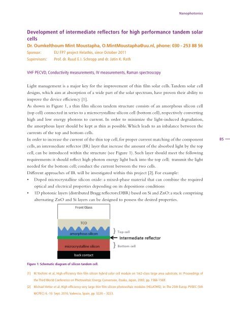
As shown in Figure 1, a thin film silicon tandem structure consists of an amorphous silicon cell<br />
(top cell) connected in series to a microcrystalline silicon cell (bottom cell), respectively converting<br />
high and low energy photons to current. In order to minimize the light-induced degradation,<br />
the amorphous layer should be kept as thin as possible. Which leads to an inbalance between the<br />
currents of the top and bottom cells.<br />
In order to increase the current of the thin top cell, <strong>for</strong> proper current matching of the component<br />
cells, an intermediate reflector (IR) layer that increase the amount of the absorbed light by the top<br />
cell, can be introduced within the structure (see Figure 1). Such layer should meet the following<br />
requirements: it should reflect high photon energy light back into the top cell; transmit the light<br />
needed <strong>for</strong> the bottom cell; conduct the current between the two cells.<br />
Different approaches of IR will be investigated within this project [2]. For example:<br />
• Doped microcrystalline silicon oxide: a mixed-phase material that can combine the required<br />
optical and electrical properties depending on its depositions conditions<br />
• 1D photonic layers (distributed Bragg reflectors:DBR) based on Si and ZnO: a stack comprising<br />
alternating ZnO and Si layers can be designed to possess the desired properties.<br />
Figure 1: Schematic diagram of silicon tandem cell.<br />
[1] M.Yoshimi et al, High efficiency thin film silicon hybrid solar cell module on 1m2-class large area substrate, in: Proceedings of<br />
the Third World Conference on Photovoltaic Energy Conversion, Osaka, Japan, 2003, pp. 1566-1569.<br />
[2] Michael Vetter et al, High efficiency very large thin film silicon photovoltaic modules (HELATHIS), in: The 25th Europ. PVSEC (5th<br />
WCPEC) 6.-10. Sept. 2010, Valencia, Spain, pp. 3220 – 3223.<br />
85