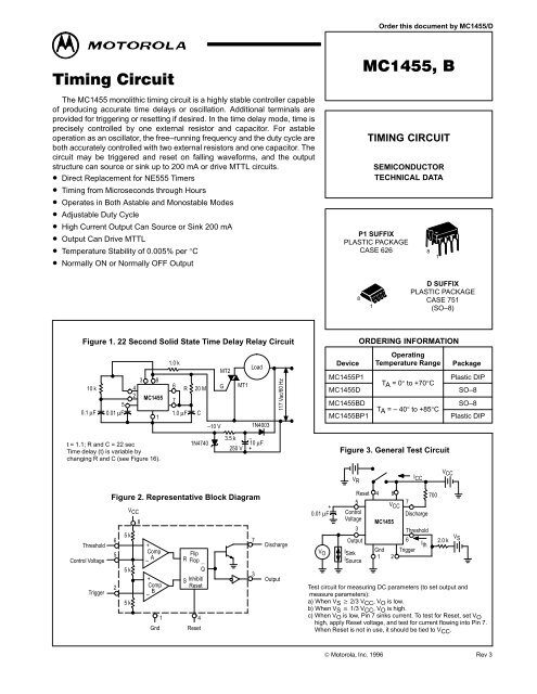
MC1455, B Timing Circuit - Rose-Hulman
MC1455, B Timing Circuit - Rose-Hulman
MC1455, B Timing Circuit - Rose-Hulman

Create successful ePaper yourself
Turn your PDF publications into a flip-book with our unique Google optimized e-Paper software.
������ �������<br />
The <strong>MC1455</strong> monolithic timing circuit is a highly stable controller capable<br />
of producing accurate time delays or oscillation. Additional terminals are<br />
provided for triggering or resetting if desired. In the time delay mode, time is<br />
precisely controlled by one external resistor and capacitor. For astable<br />
operation as an oscillator, the free–running frequency and the duty cycle are<br />
both accurately controlled with two external resistors and one capacitor. The<br />
circuit may be triggered and reset on falling waveforms, and the output<br />
structure can source or sink up to 200 mA or drive MTTL circuits.<br />
• Direct Replacement for NE555 Timers<br />
• <strong>Timing</strong> from Microseconds through Hours<br />
• Operates in Both Astable and Monostable Modes<br />
• Adjustable Duty Cycle<br />
• High Current Output Can Source or Sink 200 mA<br />
• Output Can Drive MTTL<br />
• Temperature Stability of 0.005% per °C<br />
• Normally ON or Normally OFF Output<br />
Figure 1. 22 Second Solid State Time Delay Relay <strong>Circuit</strong><br />
10 k<br />
5<br />
0.1 μF 0.01 μF<br />
4<br />
2<br />
3 8<br />
t = 1.1; R and C = 22 sec<br />
Time delay (t) is variable by<br />
changing R and C (see Figure 16).<br />
Threshold<br />
Control Voltage<br />
Trigger<br />
1.0 k<br />
Figure 2. Representative Block Diagram<br />
6<br />
5<br />
2<br />
5 k<br />
5 k<br />
5 k<br />
V CC<br />
MOTOROLA ANALOG IC DEVICE DATA<br />
8<br />
<strong>MC1455</strong><br />
1<br />
+<br />
Comp<br />
A<br />
–<br />
+<br />
Comp<br />
–<br />
B<br />
6<br />
7<br />
R<br />
1.0 μF C<br />
R<br />
S<br />
MT2<br />
20 M G MT1<br />
1N4740<br />
Flip<br />
Flop<br />
Q<br />
Inhibit/<br />
Reset<br />
1<br />
4<br />
Gnd Reset<br />
–10 V<br />
3.5 k<br />
250 V<br />
Load<br />
1N4003<br />
–<br />
10 μF<br />
+<br />
7<br />
3<br />
117 Vac/60 Hz<br />
Discharge<br />
Output<br />
+<br />
0.01 μF<br />
V O<br />
Device<br />
<strong>MC1455</strong>P1<br />
<strong>MC1455</strong>D<br />
Order this document by <strong>MC1455</strong>/D<br />
������� �<br />
TIMING CIRCUIT<br />
SEMICONDUCTOR<br />
TECHNICAL DATA<br />
P1 SUFFIX<br />
PLASTIC PACKAGE<br />
CASE 626<br />
8<br />
1<br />
ORDERING INFORMATION<br />
Operating<br />
Temperature Range Package<br />
TA = 0° to +70°C<br />
Plastic DIP<br />
SO–8<br />
<strong>MC1455</strong>BD SO–8<br />
TA = – 40° to +85°C<br />
<strong>MC1455</strong>BP1 Plastic DIP<br />
8<br />
1<br />
D SUFFIX<br />
PLASTIC PACKAGE<br />
CASE 751<br />
(SO–8)<br />
Figure 3. General Test <strong>Circuit</strong><br />
VR ICC VCC Reset 4 8<br />
700<br />
7<br />
Discharge<br />
Threshold<br />
6<br />
Ith 2.0 k V 5<br />
Control<br />
Voltage<br />
VCC <strong>MC1455</strong><br />
3<br />
Output<br />
ISink ISource Gnd<br />
1 2<br />
Trigger<br />
S<br />
Test circuit for measuring DC parameters (to set output and<br />
measure parameters):<br />
a) When V S � 2/3 V CC , V O is low.<br />
b) When V S � 1/3 V CC , V O is high.<br />
c) When V O is low, Pin 7 sinks current. To test for Reset, set V O<br />
c) high, apply Reset voltage, and test for current flowing into Pin 7.<br />
c) When Reset is not in use, it should be tied to V CC .<br />
© Motorola, Inc. 1996 Rev 3<br />
1
<strong>MC1455</strong>, B<br />
MAXIMUM RATINGS (TA = +25°C, unless otherwise noted.)<br />
Rating Symbol Value Unit<br />
Power Supply Voltage VCC +18 Vdc<br />
Discharge Current (Pin 7) I7 200 mA<br />
Power Dissipation (Package Limitation)<br />
P1 Suffix, Plastic Package<br />
Derate above TA = +25°C<br />
D Suffix, Plastic Package<br />
Derate above TA = +25°C<br />
Operating Temperature Range (Ambient)<br />
<strong>MC1455</strong>B<br />
<strong>MC1455</strong><br />
PD<br />
PD<br />
TA<br />
625<br />
5.0<br />
625<br />
160<br />
–40 to +85<br />
0 to +70<br />
mW<br />
mW/°C<br />
mW<br />
°C/W<br />
Storage Temperature Range Tstg –65 to +150 °C<br />
ELECTRICAL CHARACTERISTICS (TA = +25°C, VCC = +5.0 V to +15 V, unless otherwise noted.)<br />
Characteristics Symbol Min Typ Max Unit<br />
Operating Supply Voltage Range VCC 4.5 – 16 V<br />
Supply Current<br />
VCC = 5.0 V, RL = �<br />
VCC = 15 V, RL = �, Low State (Note 1)<br />
<strong>Timing</strong> Error (R = 1.0 kΩ to 100 kΩ) (Note 2)<br />
Initial Accuracy C = 0.1 μF<br />
Drift with Temperature<br />
Drift with Supply Voltage<br />
Threshold Voltage/Supply Voltage Vth/VCC – 2/3 –<br />
Trigger Voltage<br />
VCC = 15 V<br />
VCC = 5.0 V<br />
Trigger Current IT – 0.5 – μA<br />
Reset Voltage VR 0.4 0.7 1.0 V<br />
Reset Current IR – 0.1 – mA<br />
Threshold Current (Note 3) Ith – 0.1 0.25 μA<br />
Discharge Leakage Current (Pin 7) Idischg – – 100 nA<br />
Control Voltage Level<br />
VCC = 15 V<br />
VCC = 5.0 V<br />
Output Voltage Low<br />
ISink = 10 mA (VCC = 15 V)<br />
ISink = 50 mA (VCC = 15 V)<br />
ISink = 100 mA (VCC = 15 V)<br />
ISink = 200 mA (VCC = 15 V)<br />
ISink = 8.0 mA (VCC = 5.0 V)<br />
ISink = 5.0 mA (VCC = 5.0 V)<br />
Output Voltage High<br />
VCC = 15 V (ISource = 200 mA)<br />
VCC = 15 V (ISource = 100 mA)<br />
VCC = 5.0 V (ISource = 100 mA)<br />
2 MOTOROLA ANALOG IC DEVICE DATA<br />
ICC<br />
VT<br />
VCL<br />
VOL<br />
VOH<br />
°C<br />
–<br />
–<br />
–<br />
–<br />
–<br />
–<br />
–<br />
9.0<br />
2.6<br />
–<br />
–<br />
–<br />
–<br />
–<br />
–<br />
–<br />
12.75<br />
2.75<br />
Rise Time Differential Output tr – 100 – ns<br />
Fall Time Differential Output tf – 100 – ns<br />
NOTES: 1. Supply current when output is high is typically 1.0 mA less.<br />
2. Tested at V CC = 5.0 V and V CC = 15 V Monostable mode.<br />
3. This will determine the maximum value of R A + R B for 15 V operation. The maximum total R = 20 mΩ .<br />
3.0<br />
10<br />
1.0<br />
50<br />
0.1<br />
5.0<br />
1.67<br />
10<br />
3.33<br />
0.1<br />
0.4<br />
2.0<br />
2.5<br />
–<br />
0.25<br />
12.5<br />
13.3<br />
3.3<br />
6.0<br />
15<br />
–<br />
–<br />
–<br />
–<br />
–<br />
11<br />
4.0<br />
0.25<br />
0.75<br />
2.5<br />
–<br />
–<br />
0.35<br />
–<br />
–<br />
–<br />
mA<br />
%<br />
PPM/°C<br />
%/V<br />
V<br />
V<br />
V<br />
V
PW, PULSE WIDTH (ns min)<br />
V CC –V OH (Vdc)<br />
V OL , LOW OUTPUT VOLTAGE (Vdc)<br />
150<br />
125<br />
100<br />
75<br />
50<br />
25<br />
0<br />
0<br />
2.0<br />
1.8<br />
1.6<br />
1.4<br />
1.2<br />
1.0<br />
0.8<br />
0.6<br />
0.4<br />
0.2<br />
0<br />
1.0<br />
10<br />
1.0<br />
0.1<br />
0.01<br />
1.0<br />
Figure 4. Trigger Pulse Width<br />
0.1<br />
0.2<br />
VT (min), MINIMUM TRIGGER VOLTAGE (x VCC = Vdc)<br />
Figure 6. High Output Voltage<br />
25°C<br />
ISource (mA)<br />
Figure 8. Low Output Voltage<br />
@ VCC = 10 Vdc<br />
ISink (mA)<br />
0°C<br />
25°C<br />
MOTOROLA ANALOG IC DEVICE DATA<br />
70°C<br />
0.3<br />
5.0 V ≤ VCC ≤ 15 V<br />
2.0 5.0 10 20 50 100<br />
25°C<br />
2.0 5.0 10 20 50 100<br />
<strong>MC1455</strong>, B<br />
0.4<br />
I CC , SUPPLY CURRENT (mA)<br />
V OL , LOW OUTPUT VOLTAGE (Vdc)<br />
V OL , LOW OUTPUT VOLTAGE (Vdc)<br />
10<br />
8.0<br />
6.0<br />
4.0<br />
2.0<br />
Figure 5. Supply Current<br />
0<br />
5.0 10<br />
10<br />
1.0<br />
0.1<br />
VCC, SUPPLY VOLTAGE (Vdc)<br />
Figure 7. Low Output Voltage<br />
@ VCC = 5.0 Vdc<br />
ISink (mA)<br />
Figure 9. Low Output Voltage<br />
@ VCC = 15 Vdc<br />
ISink (mA)<br />
25°C<br />
25°C<br />
0.01 1.0 2.0 5.0 10 20 50 100<br />
10<br />
1.0<br />
0.1<br />
25°C<br />
0.01<br />
1.0 2.0 5.0 10 20 50 100<br />
3<br />
15
td, DELAY TIME NORMALIZED<br />
1.015<br />
1.010<br />
1.005<br />
1.000<br />
0.995<br />
0.990<br />
Figure 10. Delay Time versus Supply Voltage<br />
0.985<br />
0 5.0<br />
10 15<br />
20<br />
VCC, SUPPLY VOLTAGE (Vdc)<br />
, PROPAGATION DELAY TIME (ns)<br />
t pd<br />
300<br />
250<br />
200<br />
150<br />
100<br />
50<br />
0<br />
0<br />
0°C<br />
70°C<br />
<strong>MC1455</strong>, B<br />
Figure 12. Propagation Delay<br />
versus Trigger Voltage<br />
25°C<br />
0.1 0.2 0.3 0.4<br />
VT (min), MINIMUM TRIGGER VOLTAGE (x VCC = Vdc)<br />
Figure 11. Delay Time versus Temperature<br />
TA, AMBIENT TEMPERATURE (°C)<br />
4 MOTOROLA ANALOG IC DEVICE DATA<br />
td, DELAY TIME NORMALIZED<br />
1.015<br />
1.010<br />
1.005<br />
1.000<br />
0.995<br />
0.990<br />
0.985<br />
– 75 – 50 – 25 0 25 50 75 100 125
VCC<br />
Threshold<br />
Trigger<br />
Reset<br />
Discharge<br />
Gnd<br />
Reset<br />
MOTOROLA ANALOG IC DEVICE DATA<br />
<strong>MC1455</strong>, B<br />
Figure 13. Representative <strong>Circuit</strong> Schematic<br />
Threshold<br />
Comparator<br />
4.7 k 830 4.7 k<br />
10 k<br />
Discharge<br />
100<br />
Trigger<br />
Comparator<br />
100 k 5.0 k<br />
The <strong>MC1455</strong> is a monolithic timing circuit which uses an<br />
external resistor – capacitor network as its timing element. It<br />
can be used in both the monostable (one–shot) and astable<br />
modes with frequency and duty cycle controlled by the<br />
capacitor and resistor values. While the timing is dependent<br />
upon the external passive components, the monolithic circuit<br />
provides the starting circuit, voltage comparison and other<br />
functions needed for a complete timing circuit. Internal to the<br />
integrated circuit are two comparators, one for the input<br />
signal and the other for capacitor voltage; also a flip–flop and<br />
digital output are included. The comparator reference<br />
voltages are always a fixed ratio of the supply voltage thus<br />
providing output timing independent of supply voltage.<br />
Monostable Mode<br />
In the monostable mode, a capacitor and a single resistor<br />
are used for the timing network. Both the threshold terminal<br />
and the discharge transistor terminal are connected together<br />
in this mode (refer to circuit in Figure 14). When the input<br />
voltage to the trigger comparator falls below 1/3 VCC, the<br />
comparator output triggers the flip–flop so that its output sets<br />
low. This turns the capacitor discharge transistor “off” and<br />
drives the digital output to the high state. This condition<br />
allows the capacitor to charge at an exponential rate which is<br />
set by the RC time constant. When the capacitor voltage<br />
reaches 2/3 VCC, the threshold comparator resets the<br />
flip–flop. This action discharges the timing capacitor and<br />
returns the digital output to the low state. Once the flip–flop<br />
has been triggered by an input signal, it cannot be retriggered<br />
1.0 k<br />
5.0 k<br />
Control Voltage<br />
c b<br />
5.0 k e 4.7 k<br />
GENERAL OPERATION<br />
Flip–Flop Output<br />
7.0 k<br />
6.8 k<br />
c<br />
220<br />
4.7 k<br />
3.9 k<br />
b<br />
Output<br />
until the present timing period has been completed. The time<br />
that the output is high is given by the equation t = 1.1 RA C.<br />
Various combinations of R and C and their associated times<br />
are shown in Figure 16. The trigger pulse width must be less<br />
than the timing period.<br />
A reset pin is provided to discharge the capacitor, thus<br />
interrupting the timing cycle. As long as the reset pin is low,<br />
the capacitor discharge transistor is turned “on” and prevents<br />
the capacitor from charging. While the reset voltage is<br />
applied the digital output will remain the same. The reset pin<br />
should be tied to the supply voltage when not in use.<br />
RL<br />
Figure 14. Monostable <strong>Circuit</strong><br />
Output<br />
3<br />
RL 2<br />
Trigger<br />
+VCC (5.0 V to 15 V)<br />
Reset VCC<br />
4<br />
8<br />
<strong>MC1455</strong><br />
1<br />
Discharge<br />
7<br />
RA<br />
6<br />
Threshold<br />
C<br />
5<br />
Control<br />
Voltage 0.01 μF<br />
5
<strong>MC1455</strong>, B<br />
Figure 15. Monostable Waveforms Figure 16. Time Delay<br />
t = 50 μs/cm<br />
(RA = 10 kΩ, C = 0.01 μF, RL = 1.0 kΩ, VCC = 15 V)<br />
RL<br />
RL<br />
Figure 17. Astable <strong>Circuit</strong> Figure 18. Astable Waveforms<br />
Output<br />
3<br />
Trigger<br />
2<br />
+VCC (5.0 V to 15 V)<br />
Reset VCC<br />
4<br />
8<br />
<strong>MC1455</strong><br />
1<br />
7 Discharge<br />
6 Threshold<br />
5<br />
Control<br />
Voltage<br />
Astable Mode<br />
In the astable mode the timer is connected so that it will<br />
retrigger itself and cause the capacitor voltage to oscillate<br />
between 1/3 VCC and 2/3 VCC. See Figure 17.<br />
The external capacitor changes to 2/3 VCC through RA and<br />
RB and discharges to 1/3 VCC through RB. By varying the ratio<br />
of these resistors the duty cycle can be varied. The charge and<br />
discharge times are independent of the supply voltage.<br />
The charge time (output high) is given by:<br />
t1 = 0.695 (RA + RB) C<br />
The discharge time (output low) is given by:<br />
t2 = 0.695 (RB) C<br />
Thus the total period is given by:<br />
T = t1 + t2 = 0.695 (RA +2RB) C<br />
1 1.44<br />
The frequency of oscillation is then: f = =<br />
T (RA +2RB) C<br />
and may be easily found as shown in Figure 19.<br />
RB<br />
The duty cycle is given by: DC =<br />
RA +2RB<br />
To obtain the maximum duty cycle RA must be as small as<br />
possible; but it must also be large enough to limit the<br />
RA<br />
RB<br />
C<br />
6 MOTOROLA ANALOG IC DEVICE DATA<br />
C, CAPACITANCE ( μF)<br />
100<br />
10<br />
1.0<br />
0.1<br />
0.01<br />
0.001<br />
10 μs 100 μs 1.0 ms 10 ms 100 ms 1.0 10 100<br />
td, TIME DELAY (s)<br />
t = 20 μs/cm<br />
(RA = 5.1 kΩ, C = 0.01 μF, RL = 1.0 kΩ; RB = 3.9 kΩ, VCC = 15 V)<br />
discharge current (Pin 7 current) within the maximum rating<br />
of the discharge transistor (200 mA).<br />
The minimum value of RA is given by:<br />
C, CAPACITANCE ( μF)<br />
100<br />
10<br />
1.0<br />
0.1<br />
0.01<br />
RA ≥ VCC (Vdc)<br />
≥<br />
I7 (A)<br />
VCC (Vdc)<br />
0.2<br />
Figure 19. Free Running Frequency<br />
(RA + 2 RB)<br />
0.001<br />
0.1 1.0 10 100 1.0 k 10 k 100 k<br />
f, FREE RUNNING FREQUENCY (Hz)
Linear Voltage Ramp<br />
In the monostable mode, the resistor can be replaced by a<br />
constant current source to provide a linear ramp voltage. The<br />
capacitor still charges from 0 VCC to 2/3 VCC. The linear ramp<br />
time is given by:<br />
t = 2<br />
3<br />
VCC<br />
1 , where I = VCC – VB – VBE<br />
RE<br />
If VB is much larger than VBE, then t can be made<br />
independent of VCC.<br />
Digital<br />
Output<br />
3<br />
2<br />
Trigger<br />
MOTOROLA ANALOG IC DEVICE DATA<br />
<strong>MC1455</strong>, B<br />
APPLICATIONS INFORMATION<br />
Missing Pulse Detector<br />
The timer can be used to produce an output when an input<br />
pulse fails to occur within the delay of the timer. To<br />
accomplish this, set the time delay to be slightly longer than<br />
the time between successive input pulses. The timing cycle is<br />
then continuously reset by the input pulse train until a change<br />
in frequency or a missing pulse allows completion of the<br />
timing cycle, causing a change in the output level.<br />
Figure 20. Linear Voltage Sweep <strong>Circuit</strong> Figure 21. Missing Pulse Detector<br />
Reset 4<br />
<strong>MC1455</strong><br />
1<br />
VCC<br />
8 VCC<br />
7<br />
6<br />
0.01 μF<br />
5 Sweep<br />
Output<br />
RE<br />
2N4403<br />
R1<br />
RL<br />
VE<br />
or Equiv<br />
3<br />
I<br />
VB<br />
Output<br />
Control<br />
Voltage<br />
C<br />
R2<br />
+VCC (5.0 V to 15 V)<br />
Reset<br />
4 8<br />
Discharge<br />
Figure 22. Linear Voltage Ramp Waveforms Figure 23. Missing Pulse Detector Waveforms<br />
Input<br />
Trigger<br />
<strong>MC1455</strong><br />
1<br />
VCC<br />
7<br />
Threshold<br />
6 Control<br />
5 Voltage<br />
0.01 μF<br />
t = 100 μs/cm<br />
t = 500 μs/cm<br />
(RE = 10 kΩ, R2 = 100 kΩ, R1 = 39 kΩ, C = 0.01 μF, VCC = 15 V) (RA = 2.0 kΩ, RL = 1.0 kΩ, C = 0.01 μF, VCC = 15 V)<br />
2<br />
RA<br />
C<br />
2N4403<br />
or Equiv<br />
7
Pulse Width Modulation<br />
If the timer is triggered with a continuous pulse train in the<br />
monstable mode of operation, the charge time of the<br />
capacitor can be varied by changing the control voltage at<br />
Pin 5. In this manner, the output pulse width can be<br />
modulated by applying a modulating signal that controls the<br />
threshold voltage.<br />
Output<br />
Clock<br />
Input<br />
9.1 k<br />
6<br />
7<br />
Figure 24. Pulse Width Modulator<br />
RL<br />
1.0 μF 2<br />
3<br />
2<br />
+VCC (5.0 V to 15 V)<br />
8 4<br />
<strong>MC1455</strong><br />
1<br />
4 8<br />
<strong>MC1455</strong><br />
1<br />
5<br />
3<br />
0.01 μF<br />
Load<br />
27 k<br />
0.001 μF<br />
7<br />
6<br />
5<br />
5.0 μF<br />
9.1 k<br />
RA<br />
Modulation<br />
Input<br />
6<br />
7<br />
2<br />
<strong>MC1455</strong>, B<br />
C<br />
Figure 26. Sequential Timer<br />
8 4<br />
<strong>MC1455</strong><br />
Figure 25. Pulse Width Modulation Waveforms<br />
t = 0.5 ms/cm<br />
(RA = 10 kΩ, C = 0.02 μF, VCC = 15 V)<br />
Test Sequences<br />
Several timers can be connected to drive each other for<br />
sequential timing. An example is shown in Figure 26 where<br />
the sequence is started by triggering the first timer which runs<br />
for 10 ms. The output then switches low momentarily and<br />
starts the second timer which runs for 50 ms and so forth.<br />
8 MOTOROLA ANALOG IC DEVICE DATA<br />
5<br />
3<br />
Load<br />
27 k<br />
1 5.0 μF<br />
8 4<br />
0.01 μF<br />
6<br />
5 0.01 μF<br />
0.001 μF<br />
18.2 k<br />
7<br />
2<br />
<strong>MC1455</strong><br />
1<br />
3<br />
VCC (5.0 V to 15 V)<br />
Load
8<br />
1 4<br />
F<br />
NOTE 2 –A–<br />
–T–<br />
–T–<br />
SEATING<br />
PLANE<br />
H<br />
8<br />
MOTOROLA ANALOG IC DEVICE DATA<br />
G<br />
1 4<br />
G<br />
8X D<br />
–A–<br />
5<br />
5<br />
–B–<br />
N<br />
–B–<br />
C<br />
D K<br />
0.13 (0.005) M T A M B M<br />
K<br />
4X P<br />
C<br />
SEATING<br />
PLANE<br />
0.25 (0.010) M T B S A S<br />
<strong>MC1455</strong>, B<br />
OUTLINE DIMENSIONS<br />
L<br />
P1 SUFFIX<br />
PLASTIC PACKAGE<br />
CASE 626–05<br />
ISSUE K<br />
J<br />
M<br />
0.25 (0.010) M B M<br />
M �<br />
D SUFFIX<br />
PLASTIC PACKAGE<br />
CASE 751–05<br />
(SO–8)<br />
ISSUE N<br />
R X 45�<br />
F<br />
J<br />
NOTES:<br />
1. DIMENSION L TO CENTER OF LEAD WHEN<br />
FORMED PARALLEL.<br />
2. PACKAGE CONTOUR OPTIONAL (ROUND OR<br />
SQUARE CORNERS).<br />
3. DIMENSIONING AND TOLERANCING PER ANSI<br />
Y14.5M, 1982.<br />
MILLIMETERS INCHES<br />
DIM MIN MAX MIN MAX<br />
A 9.40 10.16 0.370 0.400<br />
B 6.10 6.60 0.240 0.260<br />
C 3.94 4.45 0.155 0.175<br />
D 0.38 0.51 0.015 0.020<br />
F 1.02 1.78 0.040 0.070<br />
G 2.54 BSC 0.100 BSC<br />
H 0.76 1.27 0.030 0.050<br />
J 0.20 0.30 0.008 0.012<br />
K 2.92 3.43 0.115 0.135<br />
L 7.62 BSC 0.300 BSC<br />
M ––– 10 � ––– 10 �<br />
N 0.76 1.01 0.030 0.040<br />
NOTES:<br />
1. DIMENSIONING AND TOLERANCING PER<br />
ANSI Y14.5M, 1982.<br />
2. CONTROLLING DIMENSION: MILLIMETER.<br />
3. DIMENSIONS A AND B DO NOT INCLUDE<br />
MOLD PROTRUSION.<br />
4. MAXIMUM MOLD PROTRUSION 0.15 (0.006)<br />
PER SIDE.<br />
5. DIMENSION D DOES NOT INCLUDE DAMBAR<br />
PROTRUSION. ALLOWABLE DAMBAR<br />
PROTRUSION SHALL BE 0.127 (0.005) TOTAL<br />
IN EXCESS OF THE D DIMENSION AT<br />
MAXIMUM MATERIAL CONDITION.<br />
MILLIMETERS INCHES<br />
DIM MIN MAX MIN MAX<br />
A 4.80 5.00 0.189 0.196<br />
B 3.80 4.00 0.150 0.157<br />
C 1.35 1.75 0.054 0.068<br />
D 0.35 0.49 0.014 0.019<br />
F 0.40 1.25 0.016 0.049<br />
G 1.27 BSC 0.050 BSC<br />
J 0.18 0.25 0.007 0.009<br />
K 0.10 0.25 0.004 0.009<br />
M 0 � 7 � 0 � 7 �<br />
P 5.80 6.20 0.229 0.244<br />
R 0.25 0.50 0.010 0.019<br />
9
<strong>MC1455</strong>, B<br />
Motorola reserves the right to make changes without further notice to any products herein. Motorola makes no warranty, representation or guarantee regarding<br />
the suitability of its products for any particular purpose, nor does Motorola assume any liability arising out of the application or use of any product or circuit, and<br />
specifically disclaims any and all liability, including without limitation consequential or incidental damages. “Typical” parameters which may be provided in Motorola<br />
data sheets and/or specifications can and do vary in different applications and actual performance may vary over time. All operating parameters, including “Typicals”<br />
must be validated for each customer application by customer’s technical experts. Motorola does not convey any license under its patent rights nor the rights of<br />
others. Motorola products are not designed, intended, or authorized for use as components in systems intended for surgical implant into the body, or other<br />
applications intended to support or sustain life, or for any other application in which the failure of the Motorola product could create a situation where personal injury<br />
or death may occur. Should Buyer purchase or use Motorola products for any such unintended or unauthorized application, Buyer shall indemnify and hold Motorola<br />
and its officers, employees, subsidiaries, affiliates, and distributors harmless against all claims, costs, damages, and expenses, and reasonable attorney fees<br />
arising out of, directly or indirectly, any claim of personal injury or death associated with such unintended or unauthorized use, even if such claim alleges that<br />
Motorola was negligent regarding the design or manufacture of the part. Motorola and are registered trademarks of Motorola, Inc. Motorola, Inc. is an Equal<br />
Opportunity/Affirmative Action Employer.<br />
How to reach us:<br />
USA / EUROPE / Locations Not Listed: Motorola Literature Distribution; JAPAN: Nippon Motorola Ltd.; Tatsumi–SPD–JLDC, 6F Seibu–Butsuryu–Center,<br />
P.O. Box 20912; Phoenix, Arizona 85036. 1–800–441–2447 or 602–303–5454 3–14–2 Tatsumi Koto–Ku, Tokyo 135, Japan. 03–81–3521–8315<br />
MFAX: RMFAX0@email.sps.mot.com – TOUCHTONE 602–244–6609 ASIA/PACIFIC: Motorola Semiconductors H.K. Ltd.; 8B Tai Ping Industrial Park,<br />
INTERNET: http://Design–NET.com 51 Ting Kok Road, Tai Po, N.T., Hong Kong. 852–26629298<br />
10 MOTOROLA ANALOG IC DEVICE DATA<br />
◊<br />
<strong>MC1455</strong>/D<br />
����������