ptfe wettability for electroless copper and direct metalization - Quasys
ptfe wettability for electroless copper and direct metalization - Quasys
ptfe wettability for electroless copper and direct metalization - Quasys

Create successful ePaper yourself
Turn your PDF publications into a flip-book with our unique Google optimized e-Paper software.
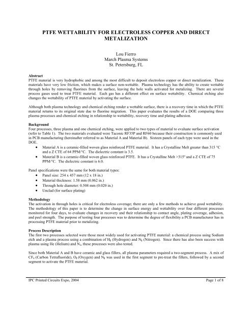
PTFE WETTABILITY FOR ELECTROLESS COPPER AND DIRECT<br />
METALIZATION<br />
Lou Fierro<br />
March Plasma Systems<br />
St. Petersburg, FL<br />
Abstract<br />
PTFE material is very hydrophobic <strong>and</strong> among the most difficult to deposit <strong>electroless</strong> <strong>copper</strong> or <strong>direct</strong> <strong>metalization</strong>. These<br />
materials have very low friction, which makes a surface non-wettable. Plasma technology has the ability to create wettable<br />
through holes by removing fluorines from the surface, leaving the hole walls activated <strong>for</strong> metalizing. There are several<br />
process gases used to treat PTFE material. Each gas has a different effect on surface <strong>wettability</strong>. Chemical etching also<br />
changes the <strong>wettability</strong> of PTFE material by activating the surface.<br />
Although both plasma technology <strong>and</strong> chemical etching render a wettable surface, there is a recovery time in which the PTFE<br />
material returns to its original state due to fluorine migration. This paper evaluates the results of a DOE comparing three<br />
plasma processes <strong>and</strong> chemical etching in relationship to <strong>wettability</strong>, recovery time <strong>and</strong> plating adhesion.<br />
Background<br />
Four processes, three plasma <strong>and</strong> one chemical etching, were applied to two types of material to evaluate surface activation<br />
(refer to Table 1). The two materials evaluated were Taconic RF35P <strong>and</strong> RF60 because their construction is commonly used<br />
in PCB manufacturing (hereinafter referred to as Material A <strong>and</strong> Material B). Sixteen panels of each type were used in the<br />
DOE.<br />
• Material A is a ceramic-filled woven glass rein<strong>for</strong>ced PTFE material. It has a Crystalline Melt greater than 315 °C<br />
<strong>and</strong> a Z CTE of 64 PPM/°C. The dielectric constant is 3.5.<br />
• Material B is a ceramic-filled woven glass rein<strong>for</strong>ced PTFE. It has a Crystalline Melt >315º <strong>and</strong> a Z CTE of 75<br />
PPM/°C. The dielectric constant is 6.0.<br />
Panel specifications were the same <strong>for</strong> both material types:<br />
• Panel size: 254 x 457 mm (12 x 18 in.)<br />
• Material thickness: 1.58 mm (0.062 in.)<br />
• Through hole diameter: 0.508 mm (0.020 in.)<br />
• Unclad (<strong>for</strong> surface plating)<br />
Methodology<br />
The activation in through holes is critical <strong>for</strong> <strong>electroless</strong> coverage; there are only a few methods to achieve good <strong>wettability</strong>.<br />
The methodology of this paper is to determine the change in surface energy <strong>and</strong> <strong>wettability</strong> over four different processes<br />
monitored <strong>for</strong> four days, to evaluate changes in recovery <strong>and</strong> their relationship to contact angle, plating coverage, adhesion,<br />
<strong>and</strong> peel strength. The purpose of testing four processes was to determine the degree of flexibility a PCB manufacturer has in<br />
processing PTFE material prior to metalizing.<br />
Process Description<br />
The first two processes selected were those most widely used <strong>for</strong> activating PTFE material: a chemical process using Sodium<br />
etch <strong>and</strong> a plasma process using a combination of H2 (Hydrogen) <strong>and</strong> N2 (Nitrogen). Since there has also been success with<br />
plasma using He (Helium) <strong>and</strong> N2, these processes were also tested.<br />
Since both Material A <strong>and</strong> B have ceramic <strong>and</strong> glass fillers, all plasma parameters required a two-segment process. A mix of<br />
CF4 (Carbon Tetrafluoride), O2 (Oxygen) <strong>and</strong> N2 was used in the first segment to pre-treat the fillers, followed by a second<br />
segment to activate the PTFE material.<br />
IPC Printed Circuits Expo, 2004 Page 1 of 8
Table 1 - Summary of DOE Processes<br />
PLASMA GAS FLOW POWER FREQUENCY TIME<br />
Process 1 H2/N2 2 SLM 4000W 40 KHz 25<br />
Process 2 100% He 2 SLM 4000W 40 KHz 25<br />
Process 3 100% N2 2 SLM 4000W 40 KHz 25<br />
Process 4 Sodium 2 min Agitation in Sodium etch followed by an alcohol <strong>and</strong><br />
hot water rinse<br />
Data Recording<br />
All the panels of Material A <strong>and</strong> B were processed on the same day. On four consecutive days, four panels of Material A <strong>and</strong><br />
four panels of Material B (representing the four processes) were released to plating. On each day, the panels were plated over<br />
the 4-day period, <strong>and</strong> the contact angle <strong>and</strong> surface energy data was recorded <strong>for</strong> cross-reference to plating results. The<br />
plating process used was Formaldehyde <strong>electroless</strong> <strong>copper</strong> followed by an acid-based electroplate <strong>copper</strong> with an average<br />
thickness of 18-µm (0.0007 in.).<br />
Metrology<br />
1. Contact Angle: the angle <strong>for</strong>med by a droplet in contact with a solid surface, measured by a goniometer prior to plating.<br />
Contact angle measurement can be used to quantify surface wetting. High contact angle (water beading) indicates that<br />
the material has a low surface energy <strong>and</strong> poor wetting characteristics. Values greater than 90° are common <strong>for</strong><br />
untreated PTFE surfaces. Low contact angles indicate good wetting characteristics. Values below 60° can be achieved<br />
on properly treated PTFE surfaces.<br />
2. Surface Energy: the ability of a surface to attract a liquid, measured in units of Dyne. Water has a surface energy of<br />
about 70 Dyne/cm. Untreated PTFE material has a surface energy below 20 Dyne/cm. Higher surface energies indicate<br />
better <strong>wettability</strong>. Each of the four processes has the capability of increasing the surface energy. Typically, surface<br />
energy values of 50 Dyne/cm are considered wettable.<br />
3. Back Lighting: after all panels were plated, each was evaluated with black back lighting to determine if any of the<br />
processes had allowed voiding.<br />
4. Plating Adhesion: the second evaluation after plating was pressure-sensitive tape testing to check <strong>for</strong> adhesion. Tape<br />
measuring 12.7 x 50.8 mm was placed on the plated surface, <strong>and</strong> then pulled in a rapid motion at a 90º angle.<br />
5. Solder Float: following tape testing, two coupons from each panel were solder floated at 550 ºF <strong>for</strong> 10 seconds. After<br />
solder floating, the coupons were micro-sectioned <strong>and</strong> evaluated <strong>for</strong> hole wall pull-away.<br />
6. Peel Strength: the final evaluation on each of the plated panels was peel strength. A Tinius Olsen Lo-Cap tensile tester<br />
was used to determine the peel strength with an applied range of 6 lbs. <strong>and</strong> a constant pull rate of 2 lbs/min. The peel<br />
strength data was used to compare the results of all four processes, not to establish acceptable or rejectable limits.<br />
Results<br />
1. Contact Angle Measurement:<br />
The untreated Material A <strong>and</strong> B had contact angle measurements of 100° <strong>and</strong> 105° respectively. These contact angles<br />
were in a non-wettable range. Plating coverage <strong>and</strong> adhesion were poor on the untreated materials <strong>and</strong>, as a result, the<br />
remainder of the test could not be per<strong>for</strong>med on these untreated materials.<br />
On Day 1, all contact angles <strong>for</strong> the treated Material A <strong>and</strong> B samples measured in the wettable range. Each of the<br />
contact angles values increased over the four days. On Day 4, all four plasma processes <strong>for</strong> both Material A <strong>and</strong> B had<br />
returned to the pre-treated angles. Sodium etch had the least fluctuation in contact angles in relationship to recovery. Of<br />
the three plasma processes, the H2/N2 segment had the lowest contact angle <strong>and</strong> took the longest to recover. (Refer to<br />
Table 2 <strong>for</strong> exact contact angles.)<br />
2. Surface Energy:<br />
All Dyne measurements were less than 30 on the untreated materials, which indicates a poor surface <strong>for</strong> plating. All four<br />
processes yielded a surface energy greater than 60 Dynes on Day 1, indicating good <strong>wettability</strong> <strong>for</strong> plating. Over the<br />
4-day period, the surface energy on the He <strong>and</strong> N2 plasma processes changed to 30 <strong>and</strong> 40 Dynes, slightly above the pre-<br />
IPC Printed Circuits Expo, 2004 Page 2 of 8
treated condition. The H2/N2 plasma <strong>and</strong> sodium process held readings of greater than 60 Dynes <strong>for</strong> all four days.<br />
(Refer to Table 2 <strong>for</strong> actual surface energy measurements.)<br />
Gas Used:<br />
H2 - N2<br />
Gas Used:<br />
He<br />
Gas Used:<br />
N2<br />
Table 2 - Contact Angle Data<br />
Product Contact Contact Contact Average St<strong>and</strong>ard Dyne<br />
Angle #1 Angle #2 Angle #3<br />
Deviation Test<br />
Day 1 Material A 20 18 30 22.67 6.43 >60<br />
Day 2 Material A 55 60 67 60.67 6.03 >60<br />
Day 3 Material A 67 67 70 68.00 1.73 >60<br />
Day 4 Material A 90 90 90 90.00 0.00 >60<br />
Day 1 Material B 50 50 55 51.67 2.89 >60<br />
Day 2 Material B 60 65 70 65.00 5.00 >60<br />
Day 3 Material B 45 50 65 53.33 10.41 >60<br />
Day 4 Material B 100 100 100 100.00 0.00 >60<br />
Product Contact Contact Contact Average St<strong>and</strong>ard Dyne<br />
Angle #1 Angle #2 Angle #3<br />
Deviation Test<br />
Day 1 Material A 78 85 90 84.33 6.03 >60<br />
Day 2 Material A 90 93 95 92.67 2.52 >60<br />
Day 3 Material A 95 95 100 96.67 2.89 >60<br />
Day 4 Material A 100 100 100 100.00 0.00 >40<br />
Day 1 Material B 96 90 96 94.00 3.46 >60<br />
Day 2 Material B 95 95 100 96.67 2.89 >60<br />
Day 3 Material B 95 95 100 96.67 2.89 >55<br />
Day 4 Material B 100 105 105 103.33 2.89 >40<br />
Product Contact Contact Contact Average St<strong>and</strong>ard Dyne<br />
Angle #1 Angle #2 Angle #3<br />
Deviation Test<br />
Day 1 Material A 70 70 80 73.33 5.77 >60<br />
Day 2 Material A 95 95 98 96.00 1.73 >50<br />
Day 3 Material A 90 95 100 95.00 5.00 >40<br />
Day 4 Material A 90 90 100 93.33 5.77 >30<br />
Day 1 Material B 96 98 100 98.00 2.00 >60<br />
Day 2 Material B 95 98 100 97.67 2.52 >60<br />
Day 3 Material B 95 98 100 97.67 2.52 >50<br />
Day 4 Material B 100 100 105 101.67 2.89 >40<br />
Sodium (Na) Etch Product Contact Contact Contact Average St<strong>and</strong>ard Dyne<br />
Angle #1 Angle #2 Angle #3<br />
Deviation Test<br />
Day 1 Material A 57 60 60 59.00 1.73 >60<br />
Day 2 Material A 50 75 78 67.67 15.37 >60<br />
Day 3 Material A 60 65 60 61.67 2.89 >60<br />
Day 4 Material A 60 65 70 65.00 5.00 >60<br />
Day 1 Material B 40 40 60 46.67 11.55 >60<br />
Day 2 Material B 50 50 50 50.00 0.00 >60<br />
Day 3 Material B 62 62 62 62.00 0.00 >60<br />
Day 4 Material B 65 68 68 67.00 1.73 >60<br />
3. Back Lighting:<br />
The first evaluation after plating was per<strong>for</strong>med using backlighting. All the plated through holes were examined <strong>for</strong><br />
voiding. Even though the contact angle increased with the plasma processes over four days, there was no evidence of<br />
IPC Printed Circuits Expo, 2004 Page 3 of 8
voids after plating. The contact angle after Sodium etch remained the same <strong>and</strong> also showed no voiding. (Refer to Table<br />
3 <strong>for</strong> the results <strong>and</strong> to Figure 1 <strong>for</strong> the summary chart.)<br />
Table 3 - Back Lighting Coverage Results<br />
Gas Used: Product Coverage Gas Used: He Product Coverage<br />
H2 - N2<br />
Results (%)<br />
Results (%)<br />
Day 1 Material A 100 Day 1 Material A 100<br />
Day 2 Material A 100 Day 2 Material A 100<br />
Day 3 Material A 100 Day 3 Material A 100<br />
Day 4 Material A 100 Day 4 Material A 100<br />
Day 1 Material B 100 Day 1 Material B 100<br />
Day 2 Material B 100 Day 2 Material B 100<br />
Day 3 Material B 100 Day 3 Material B 100<br />
Day 4 Material B 100 Day 4 Material B 100<br />
Gas Used: N2 Product Coverage Sodium (Na) Product Coverage<br />
Results (%) Etch<br />
Results (%)<br />
Day 1 Material A 100 Day 1 Material A 100<br />
Day 2 Material A 100 Day 2 Material A 100<br />
Day 3 Material A 100 Day 3 Material A 100<br />
Day 4 Material A 100 Day 4 Material A 100<br />
Day 1 Material B 100 Day 1 Material B 100<br />
Day 2 Material B 100 Day 2 Material B 100<br />
Day 3 Material B 100 Day 3 Material B 100<br />
Day 4 Material B 100 Day 4 Material B 100<br />
PERCENTAGE<br />
120<br />
120<br />
100<br />
100<br />
80<br />
PERCENTAGE<br />
60<br />
40<br />
20<br />
0<br />
80<br />
60<br />
40<br />
20<br />
0<br />
DAY 1 DAY 2 DAY 3 DAY 4<br />
DAY 1 DAY 2 DAY 3 DAY 4<br />
Figure 1 - Back Lighting Coverage Results<br />
H2 H2 - N2 - N2<br />
He He<br />
N2 N2<br />
SODIUM<br />
4. Plating/Adhesion:<br />
In a normal manufacturing process, only the through holes require activating prior to plating. For this DOE, the material<br />
was unclad so plating adhesion tests could be done. However, this presented a bigger challenge <strong>for</strong> all four processes<br />
since the surface area required to activate was much greater. There was no <strong>copper</strong> left on the tape after the tape-pull test<br />
IPC Printed Circuits Expo, 2004 Page 4 of 8
<strong>for</strong> all panels. Even the processes that had both recovered in contact angle <strong>and</strong> had low surface energy after four days<br />
showed good plating adhesion.<br />
5. Solder Float:<br />
The most critical test <strong>for</strong> all four processes was solder floating. This is the method most commonly used by PCB<br />
manufacturers to determine the reliability of the plated through hole. Cross-sections of the through holes did not show<br />
any signs of hole wall pull away. Day 4 coupons looked as good as those from Day 1. This evaluation indicated that<br />
hole walls were sufficiently activated from all processes in order to plate a reliable hole even after recovery had<br />
occurred. (Refer to Figure 2 <strong>for</strong> cross-section photos.)<br />
H2N2: Day 1 H2N2: Day 4<br />
He: Day 1 He: Day 4<br />
N2: Day 1<br />
NA: Day 1<br />
N2: Day 4<br />
NA: Day 4<br />
Figure 2 - Cross Sections Following Solder Float<br />
IPC Printed Circuits Expo, 2004 Page 5 of 8
6. Peel Strength:<br />
Following the solder float, peel tests were done to establish any differences between the four processes. This data was<br />
also collected over four days. Overall, the Sodium etch had higher peel strength readings. Of the three plasma<br />
processes, He had a higher overall peel strength. The readings on Day 4 showed very little changes from Day 1, <strong>and</strong> in<br />
some cases the peel strengths were higher. This peel strength data also demonstrates that as the materials began to<br />
recover after four days, there was still sufficient <strong>wettability</strong> to allow good adhesion even on the large surface area of the<br />
unclad panels. (Refer to Table 4 <strong>and</strong> Figure 3 <strong>for</strong> Peel Strength data.)<br />
Table 4 - Peel Strength Data<br />
Reference: Test Report A030947 from Constellation Technology Corporation<br />
Material Day Peel Load (lbs) Peel Strength (lbs/in)<br />
A-H2N2 1 0.73 2.92<br />
A-He 1 1.16 4.64<br />
A-N2 1 0.66 2.64<br />
A-Na 1 1.01 4.04<br />
B-H2N2 1 0.72 2.88<br />
B-He 1 0.93 3.72<br />
B-N2 1 0.72 2.88<br />
B-Na 1 1.42 5.68<br />
Material Day Peel Load (lbs) Peel Strength (lbs/in)<br />
A-H2N2 2 0.47 1.88<br />
A-He 2 0.65 2.60<br />
A-N2 2 0.75 3.00<br />
A-Na 2 1.57 6.28<br />
B-H2N2 2 2.29 9.16<br />
B-He 2 0.90 3.60<br />
B-N2 2 0.78 3.12<br />
B-Na 2 1.46 5.84<br />
Material Day Peel Load (lbs) Peel Strength (lbs/in)<br />
A-H2N2 3 0.48 1.92<br />
A-He 3 0.66 2.64<br />
A-N2 3 0.61 2.44<br />
A-Na 3 1.36 5.44<br />
B-H2N2 3 0.90 3.60<br />
B-He 3 1.26 5.04<br />
B-N2 3 1.33 5.32<br />
B-Na 3 1.08 4.32<br />
Material Day Peel Load (lbs) Peel Strength (lbs/in)<br />
A-H2N2 4 0.62 2.48<br />
A-He 4 0.89 3.56<br />
A-N2 4 0.51 2.04<br />
A-Na 4 1.20 4.80<br />
B-H2N2 4 1.39 5.56<br />
B-He 4 1.39 5.56<br />
B-N2 4 1.04 4.16<br />
B-Na 4 1.76 7.04<br />
IPC Printed Circuits Expo, 2004 Page 6 of 8
POUNDS PER INCH<br />
10<br />
9<br />
8<br />
7<br />
6<br />
5<br />
4<br />
3<br />
2<br />
1<br />
0<br />
PEEL STRENGTH<br />
Day 1 Day 2 Day 3 Day 4<br />
Mat'l - Process Day 1 Day 2 Day 3 Day 4<br />
A-H2N2 2.92 1.88 1.92 2.48<br />
A-He 4.64 2.60 2.64 3.56<br />
A-N2 2.64 3.00 2.44 2.04<br />
A-Na 4.04 6.28 5.44 4.80<br />
B- H2N2 2.88 9.16 3.60 5.56<br />
B-He 3.72 3.60 5.04 5.56<br />
B- N2 2.88 3.12 5.32 4.16<br />
B-Na 5.68 5.84 4.32 7.04<br />
Figure 3 - Peel Strength<br />
A-H2N2<br />
Summary<br />
The purpose of this DOE was to review several processes used to activate PTFE material to determine which was best in<br />
manufacturing PTFE panels. Most manufacturers of PTFE panels are familiar with chemical processing <strong>for</strong> activating<br />
through holes. However, plasma technologies offer an environmentally benign process that is now preferred over a chemical<br />
process. As mentioned throughout this paper, since the material used was unclad, it presented a very difficult surface to<br />
activate based on the total area that was plated. Of all the processes, the plasma H2/N2 had the lowest contact angle on Day 1.<br />
However, all plasma processes continued to recover over the four days. Sodium etch did not have as low a contact angle, but<br />
also did not recover from the reading on Day 1. Based on the data collected, all the processes had sufficiently activated the<br />
surface to allow good <strong>wettability</strong> <strong>for</strong> plating regardless of the recovery. This indicates that the contact angle need only be<br />
slightly lowered to achieve sufficient <strong>wettability</strong> <strong>for</strong> plating. The data collected over four days also gives an indication of<br />
how long panels can be held prior to plating.<br />
Please note: This study was based on two different types of rein<strong>for</strong>ced PTFE material; other constructions may not have the<br />
same results. However, based on this DOE, a PCB manufacturer has the option to choose a chemical process or one of<br />
several plasma processes to activate PTFE materials.<br />
IPC Printed Circuits Expo, 2004 Page 7 of 8<br />
A-He<br />
A-N2<br />
A-Na<br />
B-H2N2<br />
B-He<br />
B-N2<br />
B-Na
Acknowledgments:<br />
1. Drill: Kyocera/Tycom, Irvine, CA<br />
2. Plating, solder floating: Future Circuits, St. Petersburg, FL<br />
3. Peel strength: Constellation Technologies Corporation, Largo, FL<br />
4. Sodium etch: Tyco Electronics, Staf<strong>for</strong>d Springs, CT<br />
Biography<br />
Lou Fierro manages applications <strong>and</strong> contract services at March Plasma Systems' Florida facility. He is responsible <strong>for</strong><br />
process development, technical support, <strong>and</strong> plasma contract services. Lou has worked in the printed circuit industry <strong>for</strong> over<br />
20 years.<br />
March Plasma Systems<br />
12000 28 th Street North<br />
St. Petersburg, FL 33716<br />
Phone: 727-573-4567<br />
Email: lfierro@marchplasma.com<br />
IPC Printed Circuits Expo, 2004 Page 8 of 8