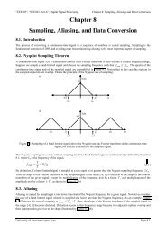
LJ Technical Systems - Staff Home Pages
LJ Technical Systems - Staff Home Pages
LJ Technical Systems - Staff Home Pages

Create successful ePaper yourself
Turn your PDF publications into a flip-book with our unique Google optimized e-Paper software.
© <strong>LJ</strong> <strong>Technical</strong> <strong>Systems</strong><br />
This publication is copyright and no part<br />
of it may be adapted or reproduced in<br />
any material form except with the prior<br />
written permission of <strong>LJ</strong> <strong>Technical</strong> <strong>Systems</strong>.<br />
Issue Number: MT191/B<br />
Written by: J Crisp<br />
<strong>LJ</strong> <strong>Technical</strong> <strong>Systems</strong><br />
An Introduction to<br />
Analog Communications<br />
Student Workbook<br />
AT02<br />
<strong>LJ</strong> <strong>Technical</strong> <strong>Systems</strong> Ltd.<br />
Francis Way<br />
Bowthorpe Industrial Estate<br />
Norwich. NR5 9JA. England<br />
Telephone: (01603) 748001<br />
Fax: (01603) 746340<br />
MT191/B<br />
<strong>LJ</strong> <strong>Technical</strong> <strong>Systems</strong> Inc.<br />
85, Corporate Drive, Holtsville,<br />
11742-2007, New York, USA.<br />
Telephone: (631) 758 1616<br />
Fax: (631) 758 1788
AT02 An Introduction to Analog Communications<br />
Student Workbook About this Student Workbook<br />
About this Student Workbook<br />
Introduction<br />
This Student Workbook has been designed to provide you with a record of your<br />
learning and achievement. It provides you with:<br />
● A Pre-Test which assesses your understanding of the terms and definitions<br />
which are required to complete this AT02 learning program.<br />
● A record of the theory you will learn.<br />
● Grids on which to draw sketches and spaces to record results, as you work<br />
through the practical exercises in the Curriculum Manual.<br />
● Notes pages for each chapter covered by the Curriculum Manual. This space<br />
allows you to record those personal notes that will help your understanding.<br />
In short, your Student Workbook replaces the notes/handouts you would expect<br />
from a formal teaching session, providing the basis for future reference or revision.<br />
You should maintain it meticulously if you are to obtain maximum benefit from it<br />
during your studies and later.<br />
Computerized Assessment of Student Performance<br />
If your laboratory is equipped with the ClassAct computer managed learning<br />
system, then the system may be used to automatically monitor your progress as you<br />
work through the Pre-Test in this Student Workbook and the chapters of the<br />
Curriculum Manual.<br />
If your instructor has asked you to use this facility, then you should key in your<br />
responses to questions at your computer managed workstation.<br />
To remind you to do this, a<br />
require a keyed-in response.<br />
symbol is printed alongside questions that<br />
The following D3000 Lesson Module is available for use with the Pre-Test and the<br />
CT02 Volume 3 Curriculum Manual:<br />
D3000 Lesson Module 20.12<br />
<strong>LJ</strong> <strong>Technical</strong> <strong>Systems</strong> 1
An Introduction to Analog Communications AT02<br />
About this Student Workbook Student Workbook<br />
Getting Started<br />
About the Pre-Test<br />
● You should attempt the Pre-Test that appears opposite. Your tutor may wish<br />
to discuss with you the results of the Pre-Test, before you embark on your<br />
AT02 studies.<br />
● When your instructor feels that you have the necessary pre-requisite<br />
knowledge to begin the AT02 Curriculum Manual, you should turn to Page 1<br />
of the Curriculum Manual to begin your studies.<br />
The following Pre-Test has been designed to assess your understanding of basic<br />
electronics. You should undertake this Pre-Test before you embark on your study<br />
of the AT02 Curriculum Manual.<br />
Please Note:<br />
● Your Instructor may place a time constraint on this Pre-Test. If this is the<br />
case, then you should attempt to complete the Pre-Test within that time.<br />
● You should attempt all questions.<br />
● Do not begin the Pre-Test until told to do so by your Instructor.<br />
● If you are working in a computer managed laboratory, you should load<br />
Chapter 31 of Module 20.12 using your computer managed workstation.<br />
This will allow you to key in your responses to the Pre-Test questions at your<br />
workstation.<br />
2 <strong>LJ</strong> <strong>Technical</strong> <strong>Systems</strong>
AT02 An Introduction to Analog Communications<br />
Student Workbook Pre-Test<br />
Pre-Test<br />
For each question, select the correct option.<br />
1. The output from an XOR gate is a logic 1 only when the two inputs are<br />
at:<br />
a logic 1.<br />
b different logic levels.<br />
c logic 0.<br />
d the same logic levels.<br />
2. The characteristic shown below is that of:<br />
Impedance<br />
a a parallel tuned circuit.<br />
b a C-R series circuit.<br />
c an L-R series circuit.<br />
d a series tuned circuit.<br />
Frequency<br />
<strong>LJ</strong> <strong>Technical</strong> <strong>Systems</strong> 3
An Introduction to Analog Communications AT02<br />
Pre-Test Student Workbook<br />
3. 450kHz is the same frequency as:<br />
a 45 000Hz<br />
b a wavelength of 666m.<br />
c 0.45MHz<br />
d 2.2µHz<br />
4. The voltage at point A in the diagram below is:<br />
a -1V<br />
b +7V<br />
c +4V<br />
d +1V<br />
0V<br />
4 <strong>LJ</strong> <strong>Technical</strong> <strong>Systems</strong><br />
A<br />
5. Modulation is the process of converting the information to be<br />
transmitted into:<br />
a a form that contains the least bandwidth.<br />
b a modular system.<br />
4V<br />
3V<br />
c a form suitable for transmission over the communication system.<br />
d a signal containing the least number of sidebands.<br />
+<br />
-<br />
-<br />
+
AT02 An Introduction to Analog Communications<br />
Student Workbook Pre-Test<br />
6. A filter is able to:<br />
a remove either the high frequency components or the low frequency<br />
components but not both.<br />
b remove or attenuate certain frequency components from a complex<br />
signal.<br />
c extract a square wave from a sinusoidal signal.<br />
d convert signals from an analog form to a digital form.<br />
7. The transformer secondary in the diagram below is labeled:<br />
a a<br />
b b<br />
c c<br />
d d<br />
C D<br />
8. If the input signal had a frequency above the frequency of resonance, a<br />
parallel tuned circuit would appear to be:<br />
a capacitive.<br />
b resistive.<br />
c resonant.<br />
d inductive.<br />
<strong>LJ</strong> <strong>Technical</strong> <strong>Systems</strong> 5<br />
B<br />
A
An Introduction to Analog Communications AT02<br />
Pre-Test Student Workbook<br />
9. The collector, emitter and base are labeled:<br />
B<br />
a A, C, B respectively.<br />
b A, B, C respectively.<br />
c B, A, C respectively.<br />
d C, A, B respectively.<br />
6 <strong>LJ</strong> <strong>Technical</strong> <strong>Systems</strong><br />
C<br />
A<br />
10. In a series circuit consisting of a capacitor and a resistor, the:<br />
a voltage and current are equal.<br />
b voltage leads the current in phase.<br />
c voltage lags the current in phase.<br />
d current is at its minimum value.<br />
11. When the switch is closed, the resonance frequency will:<br />
a decrease.<br />
b become capacitive.<br />
c may not change.<br />
d increase.<br />
Switch
AT02 An Introduction to Analog Communications<br />
Student Workbook Pre-Test<br />
12. Electrical noise:<br />
a is always a sinusoidal signal.<br />
b is only caused by electrical storms.<br />
c is any unwanted signal present at the output of a system.<br />
d can be eliminated by using a screened coaxial cable.<br />
13. To measure a DC voltage level on an oscilloscope, the input selector can<br />
be set to:<br />
a either AC or DC if the trace line is first adjusted to the central position<br />
with the Y-POS. Control.<br />
b DC<br />
c GD<br />
d AC<br />
14. The frequency that is closest in value to that displayed on the<br />
oscilloscope is:<br />
a 210µHz<br />
b 1kHz<br />
c 5.4kHz<br />
d 4.8kHz<br />
Oscilloscope control settings:<br />
Y amplifier: 5mV/div.<br />
trigger: internal +ve<br />
timebase: 0.1ms/div.<br />
<strong>LJ</strong> <strong>Technical</strong> <strong>Systems</strong> 7
An Introduction to Analog Communications AT02<br />
Pre-Test Student Workbook<br />
15. Oscilloscope probes marked as X10 are used to:<br />
a ‘expand up’ low amplitude signals for easier observation.<br />
b reduce the loading effect of the oscilloscope on the circuit operation.<br />
c decrease the circuit noise by a factor of ten.<br />
d increase the oscilloscope timebase speed by a factor of ten.<br />
16. A magnetic field is always created by:<br />
a a difference in voltage between two points.<br />
b an electric current.<br />
c an open circuit.<br />
d a capacitor.<br />
17. A bandstop filter has the effect of:<br />
a allowing only a single frequency to pass through the circuit.<br />
b attenuating the frequency of 455kHz.<br />
c attenuating a band of frequencies without affecting higher or lower<br />
frequencies.<br />
d preventing music from being played.<br />
8 <strong>LJ</strong> <strong>Technical</strong> <strong>Systems</strong>
AT02 An Introduction to Analog Communications<br />
Student Workbook Pre-Test<br />
18. A current will flow in which of the following options:<br />
a<br />
b<br />
c<br />
d<br />
+4V 0V<br />
+6V +8V<br />
-2V -1V<br />
-500V 0V<br />
a only in circuit a.<br />
b only in circuit b.<br />
c only in circuits c and d.<br />
d in all of these circuits.<br />
19. The part of the symbol marked X is called the:<br />
a anode.<br />
b emitter.<br />
c cathode.<br />
d collector.<br />
<strong>LJ</strong> <strong>Technical</strong> <strong>Systems</strong> 9<br />
X
An Introduction to Analog Communications AT02<br />
Pre-Test Student Workbook<br />
20. An oscillator:<br />
a does not require an input signal.<br />
b increases the amplitude of the input signal.<br />
c removes some frequency components from the input signal.<br />
d shifts the phase of an input signal.<br />
21. Impedance is opposition to current flow caused by:<br />
a reactance.<br />
b capacitance.<br />
c a combination of resistance and a reactance.<br />
d resistance.<br />
22. The output voltage in the diagram below will:<br />
Sinusoidal<br />
Input<br />
Signal<br />
0V<br />
a lag the input voltage by an angle less than 90°.<br />
b lead the input voltage by an angle less than 90°.<br />
c be of greater amplitude than the input.<br />
d be distorted.<br />
Output<br />
10 <strong>LJ</strong> <strong>Technical</strong> <strong>Systems</strong>
AT02 An Introduction to Analog Communications<br />
Student Workbook Pre-Test<br />
23. Bandwidth is:<br />
a the quality of the music.<br />
b a broadcast signal.<br />
c the length of the antenna.<br />
d the range of frequency components within a signal.<br />
24. An electric field is said to act:<br />
a from positive to negative.<br />
b from any object to an earth potential.<br />
c in the space around any permanent magnet.<br />
d from north to south.<br />
25. A 10µF capacitor connected in series with a 20nF capacitor would result<br />
in a total capacitance:<br />
a greater than 10µF.<br />
b between 20nF and 10µF.<br />
c exactly 10µF.<br />
d less than 20nF.<br />
26. Combining two 10V sinusoidal signals which are 90° out of phase would<br />
result in a signal of amplitude:<br />
a 20V<br />
b 14.14V<br />
c 17.32V<br />
d 0V<br />
<strong>LJ</strong> <strong>Technical</strong> <strong>Systems</strong> 11
An Introduction to Analog Communications AT02<br />
Pre-Test Student Workbook<br />
27. A screened cable:<br />
a acts as a form of high pass filter to remove distortion of the waveform<br />
being broadcast.<br />
b cannot be used for music signals as it would remove all the high<br />
frequencies.<br />
c has a conducting layer around the signal carrying wire to shield it from<br />
interference.<br />
d is a conductor that has been placed out of sight.<br />
28. In an NPN bipolar transistor, the base voltage is normally:<br />
a more positive than the emitter.<br />
b at earth potential.<br />
c more positive than the collector.<br />
d less positive than the emitter.<br />
29. Two 20Ω resistors connected in parallel would offer a total resistance:<br />
a of 40Ω.<br />
b of 20Ω.<br />
c of 10Ω.<br />
d of greater than of 10Ω but less than 20Ω.<br />
30. 20% represents the same proportion as 1 in:<br />
a 100<br />
b 4<br />
c 20<br />
d 5<br />
12 <strong>LJ</strong> <strong>Technical</strong> <strong>Systems</strong>
AT02 The ANACOM 1/1 and ANACOM 1/2 Boards<br />
Student Workbook Chapter 1<br />
Chapter 1<br />
The ANACOM 1/1 and ANACOM 1/2 Boards<br />
1.1 Layout Diagram of the ANACOM 1/1 Board<br />
Figure 1<br />
<strong>LJ</strong> <strong>Technical</strong> <strong>Systems</strong> 13
The ANACOM 1/1 and ANACOM 1/2 Boards AT02<br />
Chapter 1 Student Workbook<br />
1.2 The ANACOM 1/1 Board Blocks<br />
Figure 2<br />
Audio<br />
input<br />
L<br />
J<br />
1.3 Power Input<br />
The transmitter board can be considered as five separate blocks:<br />
ANACOM 1/1<br />
DSB/SSB AM TRANSMITTER<br />
15<br />
AUDIO AMPLIFIER<br />
Modulator<br />
VOLUME HEADPHONES<br />
Antenna<br />
Switched<br />
faults<br />
Power input<br />
Transmitter<br />
output<br />
Loudspeaker<br />
These are the electrical input connections necessary to power the module. The <strong>LJ</strong><br />
<strong>Technical</strong> <strong>Systems</strong> "IC Power 60" or "System Power 90" are the recommended<br />
power supplies.<br />
Figure 3<br />
+12V 0V<br />
-12V<br />
14 <strong>LJ</strong> <strong>Technical</strong> <strong>Systems</strong>
AT02 The ANACOM 1/1 and ANACOM 1/2 Boards<br />
Student Workbook Chapter 1<br />
1.4 The Audio Input and Amplifier<br />
This circuit provides an internally generated signal that is going to be used as<br />
'information' to demonstrate the operation of the transmitter. There is also an<br />
External Audio Input facility to enable us to supply our own audio information<br />
signals. The information signal can be monitored, if required, by switching on the<br />
loudspeaker. An amplifier is included to boost the signal power to the loudspeaker.<br />
Figure 4<br />
AUDIO OSCILLATOR<br />
AMPLITUDE FREQUENCY<br />
MIN MAX MIN MAX<br />
EXTERNAL<br />
AUDIO<br />
INPUT<br />
<strong>LJ</strong> <strong>Technical</strong> <strong>Systems</strong> 15<br />
0V<br />
AUDIO<br />
INPUT<br />
SELECT<br />
14<br />
INT<br />
EXT<br />
16
The ANACOM 1/1 and ANACOM 1/2 Boards AT02<br />
Chapter 1 Student Workbook<br />
1.5 The Modulator<br />
Figure 5<br />
This section of the board accepts the information signal and generates the final<br />
signal to be transmitted.<br />
455kHz OSCILLATOR<br />
T2<br />
4 5<br />
BALANCED MODULATOR<br />
BALANCED MODULATOR & BANDPASS FILTER CIRCUIT 1<br />
BALANCE<br />
1MHz CRYSTAL OSCILLATOR<br />
CERAMIC BANDPASS FILTER<br />
DSB<br />
MODE<br />
16 <strong>LJ</strong> <strong>Technical</strong> <strong>Systems</strong><br />
19<br />
18<br />
7<br />
8<br />
T3<br />
BALANCED MODULATOR &<br />
BANDPASS FILTER CIRCUIT 2<br />
BALANCE BALANCE<br />
2<br />
21<br />
T1<br />
T4<br />
SSB
AT02 The ANACOM 1/1 and ANACOM 1/2 Boards<br />
Student Workbook Chapter 1<br />
1.6 The Transmitter Output<br />
Figure 6<br />
The purpose of this section is to amplify the modulated signal ready for<br />
transmission. The transmitter output can be connected to the receiver by a screened<br />
cable or by using the antenna provided.<br />
The on-board telescopic antenna should be fully extended to achieve the maximum<br />
range of about 4 feet (1.3m). After use, to prevent damage, the antenna should be<br />
folded down into the transit clip mounted on the ANACOM board.<br />
Antenna<br />
OUTPUT AMPLIFIER<br />
TX<br />
OUTPUT<br />
SELECT<br />
<strong>LJ</strong> <strong>Technical</strong> <strong>Systems</strong> 17<br />
12<br />
GAIN<br />
13<br />
ANT.<br />
SKT.<br />
TX. OUTPUT<br />
0V
The ANACOM 1/1 and ANACOM 1/2 Boards AT02<br />
Chapter 1 Student Workbook<br />
1.7 The Switched Faults<br />
Notes:<br />
Under the black cover, there are eight switches. These switches can be used to<br />
simulate fault conditions in various parts of the circuit. The faults are normally used<br />
one at a time, but remain safe under any conditions of use. To ensure that the<br />
ANACOM 1 boards are fully operational, all switches should be set to OFF.<br />
Access to the switches is by use of the key provided. Insert the key and turn<br />
counter-clockwise. To replace the cover, turn the key fully clockwise and then<br />
slightly counter-clockwise to release the key.<br />
Figure 7<br />
SWITCHED FAULTS<br />
.....................................................................................................................................<br />
.....................................................................................................................................<br />
.....................................................................................................................................<br />
.....................................................................................................................................<br />
.....................................................................................................................................<br />
.....................................................................................................................................<br />
.....................................................................................................................................<br />
.....................................................................................................................................<br />
.....................................................................................................................................<br />
.....................................................................................................................................<br />
18 <strong>LJ</strong> <strong>Technical</strong> <strong>Systems</strong>
AT02 The ANACOM 1/1 and ANACOM 1/2 Boards<br />
Student Workbook Chapter 1<br />
1.8 Layout Diagram of the ANACOM 1/2 Board<br />
Figure 8<br />
<strong>LJ</strong> <strong>Technical</strong> <strong>Systems</strong> 19
The ANACOM 1/1 and ANACOM 1/2 Boards AT02<br />
Chapter 1 Student Workbook<br />
1.9 The ANACOM 1/2 Board Blocks<br />
Figure 9<br />
Receiver<br />
input<br />
1.10 Power Input<br />
The receiver board can be considered as five separate blocks:<br />
ANACOM 1/2<br />
DSB/SSB AM RECEIVER<br />
Power input<br />
Receiver Audio<br />
output<br />
Switched<br />
faults<br />
These are the electrical input connections necessary to power the module. The <strong>LJ</strong><br />
<strong>Technical</strong> <strong>Systems</strong> "IC Power 60" or "System Power 90" are the recommended<br />
power supplies. If both ANACOM 1/1 and ANACOM 1/2 boards are to be used,<br />
they can be powered by the same power supply unit.<br />
Figure 10<br />
+12V 0V<br />
20 <strong>LJ</strong> <strong>Technical</strong> <strong>Systems</strong>
AT02 The ANACOM 1/1 and ANACOM 1/2 Boards<br />
Student Workbook Chapter 1<br />
1.11 The Receiver Input<br />
Figure 11<br />
Notes:<br />
RX.<br />
INPUT<br />
SELECT<br />
In this section the input signals can be connected via a screened cable or by using<br />
the antenna provided. The telescopic antenna should be used fully extended and,<br />
after use, folded down into the transit clip.<br />
ANT.<br />
SKT.<br />
RX. INPUT<br />
......................................................................................................................................<br />
......................................................................................................................................<br />
......................................................................................................................................<br />
......................................................................................................................................<br />
......................................................................................................................................<br />
......................................................................................................................................<br />
......................................................................................................................................<br />
......................................................................................................................................<br />
<strong>LJ</strong> <strong>Technical</strong> <strong>Systems</strong> 21
The ANACOM 1/1 and ANACOM 1/2 Boards AT02<br />
Chapter 1 Student Workbook<br />
1.12 The Receiver<br />
Figure 12<br />
TUNED<br />
CIRCUIT<br />
INPUTS<br />
0V<br />
The receiver amplifies the incoming signal and extracts the original audio<br />
information signal. The incoming signals can be AM broadcast signals or those<br />
originating from ANACOM 1/1.<br />
R.F. AMPLIFIER<br />
5<br />
TC1<br />
INT 6<br />
EXT<br />
7<br />
1<br />
TUNED<br />
CIRCUIT<br />
SELECT<br />
8<br />
TUNING<br />
9<br />
T1<br />
GAIN<br />
11<br />
10<br />
13<br />
14<br />
12<br />
16<br />
17<br />
0V<br />
0V<br />
MIXER<br />
15<br />
18<br />
19<br />
LOCAL OSCILLATOR<br />
41<br />
20<br />
I.F. AMPLIFIER 1<br />
T2 T3<br />
40<br />
TC2<br />
42<br />
43<br />
T5<br />
22<br />
BEAT FREQUENCY<br />
OSCILLATOR<br />
PRODUCT DETECTOR<br />
22 <strong>LJ</strong> <strong>Technical</strong> <strong>Systems</strong><br />
2<br />
21<br />
OUT<br />
IN<br />
23<br />
3<br />
24<br />
T6<br />
AGC CIRCUIT<br />
I.F. AMPLIFIER 2<br />
26<br />
T4<br />
25<br />
44 45<br />
27<br />
OFF<br />
ON<br />
4<br />
28<br />
DIODE DETECTOR<br />
29 30<br />
32<br />
33<br />
35 36<br />
34<br />
31<br />
37
AT02 The ANACOM 1/1 and ANACOM 1/2 Boards<br />
Student Workbook Chapter 1<br />
1.13 The Audio Output<br />
Figure 13<br />
The information signal from the receiver can be amplified and heard by using a set<br />
of headphones or, if required, by the loudspeaker provided.<br />
AUDIO<br />
AMPLIFIER<br />
SPEAKER<br />
OFF<br />
38 39<br />
HEAD<br />
PHONES<br />
VOLUME<br />
<strong>LJ</strong> <strong>Technical</strong> <strong>Systems</strong> 23<br />
ON<br />
0V
The ANACOM 1/1 and ANACOM 1/2 Boards AT02<br />
Chapter 1 Student Workbook<br />
1.14 The Switched Faults<br />
Notes:<br />
Under the cover, there are eight switches. These switches can be used to simulate<br />
fault conditions in various parts of the circuit. The faults are normally used one at a<br />
time, but remain safe under any conditions of use. To ensure that the ANACOM 1<br />
boards are fully operational, all switches should be set to OFF. Access to the<br />
switches is by use of the key provided. Insert the key and turn counter-clockwise.<br />
To replace the cover, turn the key fully clockwise and then slightly counterclockwise<br />
to release the key.<br />
Figure 14<br />
SWITCHED FAULTS<br />
.....................................................................................................................................<br />
.....................................................................................................................................<br />
.....................................................................................................................................<br />
.....................................................................................................................................<br />
.....................................................................................................................................<br />
.....................................................................................................................................<br />
.....................................................................................................................................<br />
.....................................................................................................................................<br />
.....................................................................................................................................<br />
.....................................................................................................................................<br />
24 <strong>LJ</strong> <strong>Technical</strong> <strong>Systems</strong>
AT02 An Introduction to Amplitude Modulation<br />
Student Workbook Chapter 2<br />
Chapter 2<br />
An Introduction to Amplitude Modulation<br />
2.1 The Frequency Components of the Human Voice<br />
Figure 15<br />
Amplitude<br />
When we speak, we generate a sound that is very complex and changes<br />
continuously so at a particular instant in time the waveform may appear as shown in<br />
Figure 15 below.<br />
However complicated the waveform looks, we can show that it is made of many<br />
different sinusoidal signals added together.<br />
time<br />
To record this information we have a choice of three methods. The first is to show<br />
the original waveform as we did in Figure 15.<br />
The second method is to make a list of all the separate sinusoidal waveforms that<br />
were contained within the complex waveform (these are called 'components', or<br />
'frequency components'). This can be seen in Figure 16 overleaf.<br />
<strong>LJ</strong> <strong>Technical</strong> <strong>Systems</strong> 25
An Introduction to Amplitude Modulation AT02<br />
Chapter 2 Student Workbook<br />
Figure 16<br />
Only four of the components of the audio signal in Figure 15 are<br />
shown above. The actual number of components depends on the shape<br />
of the signal being considered and could be a hundred or more if the<br />
waveform was very complex.<br />
The third way is to display all the information on a diagram. Such a diagram shows<br />
the frequency spectrum. It is a graph with amplitude plotted against frequency.<br />
Each separate frequency is represented by a single vertical line, the length of which<br />
represents the amplitude of the sinewave. Such a diagram is shown in Figure 17<br />
opposite. Note that nearly all speech information is contained within the frequency<br />
range of 300Hz to 3.4kHz.<br />
26 <strong>LJ</strong> <strong>Technical</strong> <strong>Systems</strong>
AT02 An Introduction to Amplitude Modulation<br />
Student Workbook Chapter 2<br />
Amplitude<br />
0 300Hz 3.4kHz<br />
Figure 17 A Typical Voice-Frequency Spectrum<br />
Frequency<br />
Although an oscilloscope will only show the original complex waveform, it is<br />
important for us to remember that we are really dealing with a group of sinewaves<br />
of differing frequencies, amplitudes and phases.<br />
2.2 A Simple Communication System<br />
Once we are out of shouting range of another person, we must rely on some<br />
communication system to enable us to pass information.<br />
The only essential parts of any communication system are a transmitter, a<br />
communication link and a receiver, and in the case of speech, this can be achieved<br />
by a length of cable with a microphone and an amplifier at one end and a<br />
loudspeaker and an amplifier at the other.<br />
Microphone<br />
Amplifier<br />
Figure 18 A Simple Communication System<br />
Communication link<br />
(a wire in this example)<br />
Amplifier<br />
Loudspeaker<br />
For long distances, or for when it is required to send signals to many destinations at<br />
the same time, it is convenient to use a radio communication system.<br />
<strong>LJ</strong> <strong>Technical</strong> <strong>Systems</strong> 27
An Introduction to Amplitude Modulation AT02<br />
Chapter 2 Student Workbook<br />
2.3 The Frequency Problem<br />
Figure 19<br />
Antenna<br />
To communicate by radio over long distances we have to send a signal between two<br />
antennas, one at the sending or transmitting end and the other at the receiver.<br />
Antenna<br />
Transmitter Receiver<br />
The frequencies used by radio systems for AM transmissions are between 200kHz<br />
and 25MHz.<br />
A typical radio frequency of, say, 1MHz is much higher than the frequencies<br />
present in the human voice.<br />
We appear to have two incompatible requirements. The radio system uses<br />
frequencies like 1MHz to transmit over long distances, but we wish to send voice<br />
frequencies of between 300Hz and 3.4kHz that are quite impossible to transmit by<br />
radio signals.<br />
28 <strong>LJ</strong> <strong>Technical</strong> <strong>Systems</strong>
AT02 An Introduction to Amplitude Modulation<br />
Student Workbook Chapter 2<br />
2.4 Modulation<br />
This problem can be overcome by using a process called 'modulation'.<br />
The radio system can easily send high frequency signals between a transmitter and a<br />
receiver but this, on its own, conveys no information.<br />
Now, if we were to switch it on and off for certain intervals, we could use it to send<br />
information. For example, we could switch it on briefly at exactly one second<br />
intervals and provide a time signal (see Figure 20 below). Messages could be passed<br />
by switching it on and off in a sequence of long and short bursts and hence send a<br />
message by Morse Code. Figure 20 below shows the sequence that would send the<br />
distress signal SOS.<br />
Figure 20<br />
A time signal<br />
An SOS distress signal<br />
One second interval<br />
The high frequency signal that has been used to send or 'carry' the information from<br />
one place to another is called a 'carrier wave'.<br />
The carrier wave must be persuaded in some way to convey the speech to the<br />
receiver. The speech signal represents the 'information' that we wish to send and<br />
therefore this signal is called the 'information signal'.<br />
The method employed is to change some characteristic of the carrier wave in<br />
sympathy with the information signal and then, by detecting this change, be able to<br />
recover the information signal at the receiver.<br />
<strong>LJ</strong> <strong>Technical</strong> <strong>Systems</strong> 29
An Introduction to Amplitude Modulation AT02<br />
Chapter 2 Student Workbook<br />
2.5 Amplitude Modulation (AM)<br />
Figure 21<br />
2.6 Depth of Modulation<br />
The method that we are going to use is called Amplitude Modulation. As the name<br />
would suggest, we are going to use the information signal to control the amplitude<br />
of the carrier wave.<br />
As the information signal increases in amplitude, the carrier wave is also made to<br />
increase in amplitude. Likewise, as the information signal decreases, then the carrier<br />
amplitude decreases.<br />
By looking at Figure 21 below, we can see that the modulated carrier wave does<br />
appear to ‘contain’ in some way the information as well as the carrier. We will see<br />
later how the receiver is able to extract the information from the amplitude<br />
modulated carrier wave.<br />
Information signal<br />
Carrier wave input<br />
Amplitude Modulator<br />
Modulated<br />
carrier wave<br />
The amount by which the amplitude of the carrier wave increases and decreases<br />
depends on the amplitude of the information signal and is called the 'depth of<br />
modulation'.<br />
The depth of modulation can be quoted as a fraction or as a percentage.<br />
Vmax− Vmin<br />
Percentage modulation =<br />
×<br />
Vmax+ Vmin<br />
100%<br />
30 <strong>LJ</strong> <strong>Technical</strong> <strong>Systems</strong>
AT02 An Introduction to Amplitude Modulation<br />
Student Workbook Chapter 2<br />
Figure 22 Depth of Modulation<br />
Here is an example:<br />
0V 6V 10V<br />
Vmin<br />
Vmax<br />
In Figure 22 we can see that the modulated carrier wave varies from a maximum<br />
peak-to-peak value of 10 volts, down to a minimum value of 6 volts.<br />
Inserting these figures in the above formula, we get:<br />
10 6<br />
Percentage modulation<br />
10 + 6 100%<br />
=<br />
−<br />
×<br />
2.7 The Frequency Spectrum<br />
4<br />
= ×<br />
16<br />
=<br />
100%<br />
25% or 0.25<br />
Assume a carrier frequency (fc) of 1MHz and an amplitude of, say, 5 volts peak-topeak.<br />
The carrier could be shown as:<br />
5V<br />
Amplitude<br />
Figure 23 The Frequency Spectrum of a Carrier Wave<br />
0<br />
1MHz<br />
Carrier<br />
Frequency<br />
<strong>LJ</strong> <strong>Technical</strong> <strong>Systems</strong> 31
An Introduction to Amplitude Modulation AT02<br />
Chapter 2 Student Workbook<br />
If we also have a 1kHz information signal, or modulating frequency (fm), with an<br />
amplitude of 2V peak-to-peak it would look like this:<br />
5V<br />
Amplitude<br />
2V<br />
0<br />
Information Signal<br />
1kHz<br />
1MHz<br />
Figure 24 The Frequency Spectrum of a Carrier Wave and an Information Signal<br />
5V<br />
Amplitude<br />
2V<br />
Carrier<br />
Frequency<br />
When both signals have passed through the amplitude modulator they are combined<br />
to produce an amplitude modulated wave.<br />
The resultant AM signal has a new frequency spectrum as shown in Figure 25<br />
below:<br />
0<br />
Lower Side Frequency<br />
Carrier<br />
Notice that the1kHz signal is no longer present<br />
Figure 25 Frequency Spectrum of Resultant AM Signal<br />
Upper Side Frequency<br />
Frequency<br />
32 <strong>LJ</strong> <strong>Technical</strong> <strong>Systems</strong>
AT02 An Introduction to Amplitude Modulation<br />
Student Workbook Chapter 2<br />
Notes:<br />
Some interesting changes have occurred as a result of the modulation process.<br />
(i) The original 1kHz information frequency has disappeared.<br />
(ii) The 1MHz carrier is still present and is unaltered.<br />
(iii) There are two new components:<br />
Carrier frequency (fc) plus the information frequency, called the upper side<br />
frequency (fc + fm)<br />
and<br />
Carrier frequency (fc) minus the information frequency, called the lower side<br />
frequency (fc - fm)<br />
The resulting signal in this example has a maximum frequency of 1001kHz and a<br />
minimum frequency of 999kHz and so it occupies a range of 2kHz. This is called<br />
the bandwidth of the signal. Notice how the bandwidth is twice the highest<br />
frequency contained in the information signal.<br />
......................................................................................................................................<br />
......................................................................................................................................<br />
......................................................................................................................................<br />
......................................................................................................................................<br />
......................................................................................................................................<br />
......................................................................................................................................<br />
......................................................................................................................................<br />
......................................................................................................................................<br />
......................................................................................................................................<br />
......................................................................................................................................<br />
......................................................................................................................................<br />
......................................................................................................................................<br />
......................................................................................................................................<br />
<strong>LJ</strong> <strong>Technical</strong> <strong>Systems</strong> 33
An Introduction to Amplitude Modulation AT02<br />
Chapter 2 Student Workbook<br />
2.8 Constructing the Amplitude Modulated Waveform<br />
20V<br />
15V<br />
10V<br />
5V<br />
0V<br />
-5V<br />
-10V<br />
-15V<br />
-20V<br />
5V<br />
0V<br />
-5V<br />
5V<br />
0V<br />
-5V<br />
Figure 26<br />
Carrier wave<br />
Upper side freq.<br />
Lower side freq.<br />
0<br />
It is often difficult to see how the AM carrier wave can actually consist of the<br />
carrier and the two side frequencies, all of which are radio frequency signals - there<br />
is no audio signal present at all. In appearance, the AM carrier wave looks more<br />
likely to consist of the carrier frequency and the incoming information signal.<br />
Figure 26 shows this situation:<br />
5 10 15 20 25 30 35 40 45<br />
time<br />
Here are the three radio frequency signals that form the modulated carrier wave.<br />
We are going to add the three components and (hopefully) reconstruct the<br />
modulated waveform.<br />
34 <strong>LJ</strong> <strong>Technical</strong> <strong>Systems</strong>
AT02 An Introduction to Amplitude Modulation<br />
Student Workbook Chapter 2<br />
Figure 27 An Amplitude Modulated Wave<br />
2.9 Sidebands<br />
<strong>LJ</strong> <strong>Technical</strong> <strong>Systems</strong> 35<br />
time<br />
If the information signal consisted of a range of frequencies, each separate<br />
frequency will create its own upper side frequency and lower side frequency.<br />
As an example, let us imagine that a carrier frequency of 1MHz is amplitude<br />
modulated by an information signal consisting of frequencies 500Hz, 1.5kHz and<br />
3kHz.<br />
As each modulating frequency produces its own upper and lower side frequency<br />
there is a range of frequencies present above and below the carrier frequency. All<br />
the upper side frequencies are grouped together and referred to as the upper<br />
sideband (USB) and all the lower side frequencies form the lower sideband (LSB).
An Introduction to Amplitude Modulation AT02<br />
Chapter 2 Student Workbook<br />
Amplitude<br />
This amplitude modulated wave would have a frequency spectrum as shown in<br />
Figure 28 below:<br />
0<br />
Lower Sideband<br />
0.997 0.9985 0.9995<br />
1MHz<br />
Carrier<br />
This diagram is not drawn to scale.<br />
Upper Sideband<br />
1.0005 1.0015 1.003<br />
Figure 28 Frequency Spectrum Showing Upper and Lower Sidebands<br />
Frequency (MHz)<br />
Because the frequency spectrum of the AM waveform contains two sidebands, this<br />
type of amplitude modulation is often called a double-sideband transmission, or<br />
DSB.<br />
2.10 Power in the Sidebands<br />
The modulated carrier wave that is finally transmitted contains the original carrier<br />
and the sidebands. The carrier wave is unaltered by the modulation process and<br />
contains at least two-thirds of the total transmitted power. The remaining power is<br />
shared between the two sidebands.<br />
The power distribution depends on the depth of modulation used and is given by:<br />
⎛ N<br />
Total power = ( carrier power)<br />
⎜1<br />
+<br />
⎝ 2<br />
Example:<br />
⎞<br />
⎟ where N is the depth of modulation.<br />
⎠<br />
A DSB AM signal with a 1kW carrier was modulated to a depth of 60%. How<br />
much power is contained in the upper sideband?<br />
(i) Start with the formula:<br />
2<br />
⎛ N ⎞<br />
Total power = ( carrier power)<br />
⎜1<br />
+ ⎟ where N is the depth of modulation.<br />
⎝ 2 ⎠<br />
36 <strong>LJ</strong> <strong>Technical</strong> <strong>Systems</strong><br />
2
AT02 An Introduction to Amplitude Modulation<br />
Student Workbook Chapter 2<br />
Notes:<br />
(ii) Insert all the figures that we know. This is the 1000 for the carrier power and<br />
0.6 for the modulation depth. We could have used the figure 60% instead of<br />
0.6 but this way makes the math slightly easier.<br />
Total power = ( 1000) 1 06 ⎛ .<br />
⎜ +<br />
⎝ 2<br />
(iii) Remove the brackets.<br />
Total power<br />
= ( 1000) 1<br />
( )<br />
W<br />
036 ⎛ .<br />
⎜ +<br />
⎝ 2<br />
= 1000 × 1+ 0. 18<br />
= 1000 × 118 .<br />
= 1180<br />
<strong>LJ</strong> <strong>Technical</strong> <strong>Systems</strong> 37<br />
2<br />
⎞<br />
⎟<br />
⎠<br />
⎞<br />
⎟<br />
⎠<br />
(iv) The carrier power was 1000W and the total power of the modulated wave is<br />
1180W so the two sidebands must, between them, contain the other 180W.<br />
The power contained in the upper and lower sidebands is always equal and so<br />
each must contain 180<br />
2<br />
= 90W.<br />
The greater the depth of modulation, the greater is the power contained within the<br />
sidebands. The highest usable depth of modulation is 100% (above this the<br />
distortion becomes excessive).<br />
Since at least twice as much power is wasted as is used, this form of modulation is<br />
not very efficient when considered on a power basis. The good news is that the<br />
necessary circuits at the transmitter and at the receiver are simple and inexpensive<br />
to design and construct.<br />
......................................................................................................................................<br />
......................................................................................................................................<br />
......................................................................................................................................<br />
......................................................................................................................................<br />
......................................................................................................................................<br />
......................................................................................................................................
An Introduction to Amplitude Modulation AT02<br />
Chapter 2 Student Workbook<br />
2.11 Practical Exercise: The Double Sideband AM Waveform<br />
The frequency and peak-to-peak voltage of the carrier are: ....................................<br />
...............................................................................................................................<br />
The frequency and peak-to-peak voltage of the information signal are: ...................<br />
...............................................................................................................................<br />
Record the AM waveform at tp3 in Figure 30 below.<br />
Volts<br />
1.2<br />
0.8<br />
0.4<br />
0V<br />
-0.4<br />
-0.8<br />
-1.2<br />
0 0.2 0.4 0.6 0.8 1.0<br />
Time (milliseconds)<br />
Figure 30 The AM Waveform at tp3 on ANACOM 1/1<br />
The effects of adjusting the AMPLITUDE PRESET and the FREQUENCY<br />
PRESET in the AUDIO OSCILLATOR are: .........................................................<br />
...............................................................................................................................<br />
...............................................................................................................................<br />
...............................................................................................................................<br />
38 <strong>LJ</strong> <strong>Technical</strong> <strong>Systems</strong>
AT02 DSB Transmitter and Receiver<br />
Student Workbook Chapter 3<br />
Chapter 3<br />
DSB Transmitter and Receiver<br />
3.1 The Double Sideband Transmitter<br />
Audio<br />
Oscillator<br />
Carrier<br />
Generator<br />
Information Signal<br />
Modulator<br />
Carrier Wave<br />
Figure 31 An Amplitude Modulated Transmitter<br />
AM Waveform<br />
Output<br />
Amplifier<br />
Antenna<br />
Amplified Output<br />
Signal<br />
The transmitter circuits produce the amplitude modulated signals that are used to<br />
carry information over the transmission path to the receiver. The main parts of the<br />
transmitter are shown in Figure 31.<br />
<strong>LJ</strong> <strong>Technical</strong> <strong>Systems</strong> 39
DSB Transmitter and Receiver AT02<br />
Chapter 3 Student Workbook<br />
In Figures 31 and 32, we can see that the peak-to-peak voltages in the AM<br />
waveform increase and decrease in sympathy with the audio signal.<br />
Figure 32 The Modulation Envelope<br />
Information signal<br />
Amplitude modulated<br />
wave<br />
The envelope<br />
To emphasize the connection between the information and the final waveform, a<br />
line is sometimes drawn to follow the peaks of the carrier wave as shown in Figure<br />
32. This shape, enclosed by a dashed line in our diagram, is referred to as an<br />
‘envelope’, or a ‘modulation envelope’. It is important to appreciate that it is only a<br />
guide to emphasize the shape of the AM waveform.<br />
We will now consider the action of each circuit as we follow the route taken by the<br />
information that we have chosen to transmit.<br />
The first task is to get hold of the information to be transmitted.<br />
3.2 The Information Signal<br />
In test situations it is more satisfactory to use a simple sinusoidal information signal<br />
since its attributes are known and of constant value. We can then measure various<br />
characteristics of the resultant AM waveform, such as the modulation depth for<br />
example. Such measurements would be very difficult if we were using a varying<br />
signal from an external source such as a broadcast station.<br />
The next step is to generate the carrier wave.<br />
40 <strong>LJ</strong> <strong>Technical</strong> <strong>Systems</strong>
AT02 DSB Transmitter and Receiver<br />
Student Workbook Chapter 3<br />
3.3 The Carrier Wave<br />
The carrier wave must meet two main criteria.<br />
It should be of a convenient frequency to transmit over the communication path in<br />
use. In a radio link transmissions are difficult to achieve at frequencies less than<br />
15kHz and few radio links employ frequencies above 10GHz. Outside of this range<br />
the cost of the equipment increases rapidly with very few advantages.<br />
Remember that although 15kHz is within the audio range, we cannot hear the radio<br />
signal because it is an electromagnetic wave and our ears can only detect waves<br />
which are due to changes of pressure.<br />
The second criterion is that the carrier wave should also be a sinusoidal waveform.<br />
Can you see why?<br />
A sinusoidal signal contains only a single frequency and when modulated by a<br />
single frequency, will give rise to just two side frequencies, the upper and the lower<br />
side frequencies. However, if the sinewave were to be a complex wave containing<br />
many different frequencies, each separate frequency component would generate its<br />
own side frequencies. The result is that the overall bandwidth occupied by the<br />
transmission would be very wide and, on the radio, would cause interference with<br />
the adjacent stations. In Figure 33 overleaf, a simple case is illustrated in which the<br />
carrier only contains three frequency components modulated by a single frequency<br />
component. Even so we can see that the overall bandwidth has been considerably<br />
increased.<br />
<strong>LJ</strong> <strong>Technical</strong> <strong>Systems</strong> 41
DSB Transmitter and Receiver AT02<br />
Chapter 3 Student Workbook<br />
Figure 33<br />
Amplitude<br />
Amplitude<br />
0<br />
A sinusoidal Carrier Wave<br />
0<br />
Carrier<br />
Frequency<br />
Total<br />
bandwidth<br />
Carrier<br />
Total<br />
bandwidth<br />
If the carrier wave contained several frequencies,<br />
each would produce its own side frequencies.<br />
Frequency<br />
On ANACOM 1/1, the carrier wave generated is a sinewave of 1MHz.<br />
Now we have the task of combining the information signal and the carrier wave to<br />
produce amplitude modulation.<br />
42 <strong>LJ</strong> <strong>Technical</strong> <strong>Systems</strong>
AT02 DSB Transmitter and Receiver<br />
Student Workbook Chapter 3<br />
3.4 The Modulator<br />
There are many different designs of amplitude modulator. They all achieve the same<br />
result. The amplitude of the carrier is increased and decreased in sympathy with the<br />
incoming information signal as we saw in Chapter 2.<br />
Information Signal<br />
Carrier Wave<br />
Modulator<br />
Figure 34 Modulation of Information Signal and Carrier Wave<br />
The signal is now nearly ready for transmission.<br />
AM Waveform<br />
If the modulation process has given rise to any unwanted frequency components<br />
then a bandpass filter can be employed to remove them.<br />
3.5 Output Amplifier (or Power Amplifier)<br />
This amplifier is used to increase the strength of the signal before being passed to<br />
the antenna for transmission. The output power contained in the signal and the<br />
frequency of transmission are the two main factors that determine the range of the<br />
transmission.<br />
<strong>LJ</strong> <strong>Technical</strong> <strong>Systems</strong> 43
DSB Transmitter and Receiver AT02<br />
Chapter 3 Student Workbook<br />
3.6 The Antenna<br />
Antenna<br />
Antenna<br />
Antenna<br />
x<br />
x<br />
x<br />
Electric<br />
Field<br />
An electromagnetic wave, such as a light ray, consists of two fields, an electric field<br />
and a magnetic field. These two fields are always at right angles to each other and<br />
move in a direction that is at right angles to both the magnetic and the electric<br />
fields, this is shown in Figure 35.<br />
Magnetic Field<br />
Electromagnetic<br />
Wave<br />
Figure 35 An Electromagnetic Wave<br />
y<br />
y<br />
y<br />
This shows the electric field<br />
moving out from the antenna. In<br />
this example the electric field is<br />
vertical because the antenna is<br />
positioned vertically (in the<br />
directionshownbyy).<br />
The magnetic field is always at<br />
right angles to the electric field<br />
so in this case, it is positioned<br />
horizontally (in the direction<br />
shown by x).<br />
In an electromagnetic wave<br />
both fields exist together and<br />
they move at the speed of light<br />
in a direction that is at right<br />
angles to both fields (shown by<br />
the arrow labeled z).<br />
The antenna converts the power output of the Output Amplifier into an<br />
electromagnetic wave.<br />
How does it do this?<br />
44 <strong>LJ</strong> <strong>Technical</strong> <strong>Systems</strong><br />
z<br />
z<br />
z
AT02 DSB Transmitter and Receiver<br />
Student Workbook Chapter 3<br />
3.7 Polarization<br />
The output amplifier causes a voltage to be generated along the antenna thus<br />
generating a voltage difference and the resultant electric field between the top and<br />
bottom. This causes an alternating movement of electrons on the transmitting<br />
antenna that is really an AC current. Since an electric current always has a magnetic<br />
field associated with it, an alternating magnetic field is produced.<br />
The overall effect is that the output amplifier has produced alternating electric and<br />
magnetic fields around the antenna. The electric and magnetic fields spread out as<br />
an electromagnetic wave at the speed of light (3 x 10 8 meters per second).<br />
For maximum efficiency the antenna should be of a precise length. The optimum<br />
size of antenna for most purposes is one having an overall length of one quarter of<br />
the wavelength of the transmitted signal.<br />
This can be found by:<br />
λ = λ<br />
v<br />
where v = speed of light, = wavelength and<br />
f<br />
f = frequency in Hertz<br />
In the case of the ANACOM 1/1, the transmitted carrier is 1MHz and so the ideal<br />
length of antenna is:<br />
λ =<br />
λ<br />
× 3 10<br />
1× 10<br />
= 300m<br />
8<br />
6<br />
One quarter of this wavelength would be 75 meters (about 245 feet).<br />
We can now see that the antenna provided on the ANACOM 1/1 is necessarily less<br />
than the ideal size!<br />
If the transmitting antenna is placed vertically, the electrical field is vertical and the<br />
magnetic field is horizontal (as seen in Figure 35). If the transmitting antenna is<br />
now moved by 90° to make it horizontal, the electrical field is horizontal and the<br />
magnetic field becomes vertical. By convention, we use the plane of the electric<br />
field to describe the orientation, or polarization, of the em (electromagnetic) wave.<br />
A vertical transmitting antenna results in a vertically polarized wave, and a<br />
horizontal one would result in a horizontally polarized em wave.<br />
<strong>LJ</strong> <strong>Technical</strong> <strong>Systems</strong> 45
DSB Transmitter and Receiver AT02<br />
Chapter 3 Student Workbook<br />
3.8 The DSB Receiver<br />
Antenna<br />
The em wave from the transmitting antenna will travel to the receiving antenna,<br />
carrying the information with it.<br />
RF Amplifier Mixer IF Amplifier IF Amplifier<br />
Diode<br />
AF Amplifier<br />
Detector<br />
Local<br />
Oscillator<br />
Figure 36 A Superheterodyne Receiver<br />
Loudspeaker<br />
We will continue to follow our information signal as it passes through the receiver.<br />
3.9 The Receiving Antenna<br />
The receiving antenna operates in the reverse mode to the transmitter antenna. The<br />
electromagnetic wave strikes the antenna and generates a small voltage in it.<br />
Ideally, the receiving antenna must be aligned to the polarization of the incoming<br />
signal so generally, a vertical transmitting antenna will be received best by using a<br />
vertical receiving antenna.<br />
The actual voltage generated in the antenna is very small - usually less than 50<br />
millivolts and often only a few microvolts. The voltage supplied to the loudspeaker<br />
at the output of the receiver is up to ten volts.<br />
We clearly need a lot of amplification.<br />
46 <strong>LJ</strong> <strong>Technical</strong> <strong>Systems</strong>
AT02 DSB Transmitter and Receiver<br />
Student Workbook Chapter 3<br />
3.10 The Radio Frequency (RF) Amplifier<br />
Notes:<br />
The antenna not only provides very low amplitude input signals but it picks up all<br />
available transmissions at the same time. This would mean that the receiver output<br />
would include all the various stations on top of each other, which would make it<br />
impossible to listen to any one transmission.<br />
The receiver circuits generate noise signals that are added to the wanted signals.<br />
We hear this as a background hiss and is particularly noticeable if the receiver is<br />
tuned between stations or if a weak station is being received.<br />
The RF amplifier is the first stage of amplification. It has to amplify the incoming<br />
signal above the level of the internally generated noise and also to start the process<br />
of selecting the wanted station and rejecting the unwanted ones.<br />
......................................................................................................................................<br />
......................................................................................................................................<br />
......................................................................................................................................<br />
......................................................................................................................................<br />
......................................................................................................................................<br />
......................................................................................................................................<br />
......................................................................................................................................<br />
......................................................................................................................................<br />
......................................................................................................................................<br />
......................................................................................................................................<br />
......................................................................................................................................<br />
......................................................................................................................................<br />
......................................................................................................................................<br />
......................................................................................................................................<br />
<strong>LJ</strong> <strong>Technical</strong> <strong>Systems</strong> 47
DSB Transmitter and Receiver AT02<br />
Chapter 3 Student Workbook<br />
3.11 Selectivity<br />
Figure 37<br />
Amplifier<br />
gain<br />
Strength of<br />
received<br />
stations<br />
Signal<br />
strength<br />
after the<br />
amplifier<br />
in mV<br />
A parallel tuned circuit has its greatest impedance at resonance and decreases at<br />
higher and lower frequencies. If the tuned circuit is included in the circuit design of<br />
an amplifier, it results in an amplifier that offers more gain at the frequency of<br />
resonance and reduced amplification above and below this frequency. This is called<br />
selectivity.<br />
5<br />
4<br />
3<br />
2<br />
1<br />
0<br />
10mV<br />
0<br />
50<br />
40<br />
30<br />
20<br />
10<br />
0<br />
800<br />
800<br />
810<br />
810<br />
Selectivity of<br />
the amplifier<br />
We have tuned the<br />
receiver to this<br />
station<br />
Frequency<br />
(kHz)<br />
Frequency<br />
(kHz)<br />
Frequency<br />
(kHz)<br />
48 <strong>LJ</strong> <strong>Technical</strong> <strong>Systems</strong><br />
820<br />
820<br />
830<br />
830<br />
840<br />
840<br />
In Figure 37 we can see the effects of using an amplifier with selectivity.
AT02 DSB Transmitter and Receiver<br />
Student Workbook Chapter 3<br />
3.12 The Local Oscillator<br />
The radio receiver is tuned to a frequency of 820kHz and, at this frequency, the<br />
amplifier provides a gain of five. Assuming the incoming signal has an amplitude of<br />
10mV as shown, its output at this frequency would be 5 x 10mV = 50mV. The<br />
stations being received at 810kHz and 830kHz each have a gain of one. With the<br />
same amplitude of 10mV, this would result in outputs of 1 x 10mV = 10mV. The<br />
stations at 800kHz and 840kHz are offered a gain of only 0.1 (approx.). This<br />
means that the output signal strength would be only 0.1 x 10mV = 1mV.<br />
The overall effect of the selectivity is that whereas the incoming signals each have<br />
the same amplitude, the outputs vary between 1mV and 50mV so we can select, or<br />
‘tune’, the amplifier to pick out the desired station.<br />
The greatest amplification occurs at the resonance frequency of the tuned circuit.<br />
This is sometimes called the center frequency.<br />
In common with nearly all radio receivers, ANACOM 1/2 adjusts the capacitor<br />
value by means of the TUNING control to select various signals.<br />
This is an oscillator producing a sinusoidal output similar to the carrier wave<br />
oscillator in the transmitter. In this case however, the frequency of its output is<br />
adjustable.<br />
The same tuning control is used to adjust the frequency of both the local oscillator<br />
and the center frequency of the RF amplifier. The local oscillator is always<br />
maintained at a frequency that is higher, by a fixed amount, than the incoming RF<br />
signals.<br />
The local oscillator frequency therefore follows, or tracks, the RF amplifier<br />
frequency.<br />
This will prove to be very useful, as we will see in the next section.<br />
3.13 The Mixer (or Frequency Changer)<br />
The mixer performs a similar function to the modulator in the transmitter.<br />
We may remember that the transmitter modulator accepts the information signal<br />
and the carrier frequency, and produces the carrier plus the upper and lower<br />
sidebands.<br />
<strong>LJ</strong> <strong>Technical</strong> <strong>Systems</strong> 49
DSB Transmitter and Receiver AT02<br />
Chapter 3 Student Workbook<br />
Figure 38 The Mixer<br />
The mixer in the receiver combines the signal from the RF amplifier and the<br />
frequency input from the local oscillator to produce three frequencies:<br />
(i) A ‘difference’ frequency of local oscillator frequency - RF signal frequency.<br />
(ii) A ‘sum’ frequency equal to local oscillator frequency + RF signal frequency.<br />
(iii) A component at the local oscillator frequency.<br />
Mixing two signals to produce such components is called a ‘heterodyne’ process.<br />
When this is carried out at frequencies above the audio spectrum, called<br />
‘supersonic’ frequencies, the type of receiver is called a ‘superheterodyne’ receiver.<br />
This is normally abbreviated to ‘superhet’. It is not a modern idea having been<br />
invented in the year 1917.<br />
From RF amplifier To IF amplifier<br />
Mixer<br />
From<br />
local oscillator<br />
In Section 3.12, we saw how the local oscillator tracks the RF amplifier so that the<br />
difference between the two frequencies is maintained at a constant value. In<br />
ANACOM 1/2 this difference is actually 455kHz.<br />
As an example, if the radio is tuned to receive a broadcast station transmitting at<br />
800kHz, the local oscillator will be running at 1.255MHz. The difference<br />
frequency is 1.255MHz - 800kHz = 455kHz.<br />
If the radio is now retuned to receive a different station being broadcast on<br />
700kHz, the tuning control re-adjusts the RF amplifier to provide maximum gain at<br />
700kHz and the local oscillator to 1.155MHz. The difference frequency is still<br />
maintained at the required 455kHz.<br />
50 <strong>LJ</strong> <strong>Technical</strong> <strong>Systems</strong>
AT02 DSB Transmitter and Receiver<br />
Student Workbook Chapter 3<br />
This frequency difference therefore remains constant regardless of the frequency to<br />
which the radio is actually tuned and is called the intermediate frequency (IF).<br />
Amplitude<br />
Figure 39 A Superhet Receiver Tuned to 800kHz<br />
3.14 Image Frequencies<br />
0<br />
IF frequency RF frequency<br />
Local oscillator<br />
frequency<br />
455 800 1255<br />
Frequency<br />
(kHz)<br />
Note: In Figure 39, the local oscillator output is shown larger than the IF and RF<br />
frequency components, this is usually the case. However, there is no fixed<br />
relationship between the actual amplitudes. Similarly, the IF and RF<br />
amplitudes are shown as being equal in amplitude but again there is no<br />
significance in this.<br />
In the last section, we saw we could receive a station being broadcast on 700kHz<br />
by tuning the local oscillator to a frequency of 1.155MHz thus giving the difference<br />
(IF) frequency of the required 455kHz.<br />
What would happen if we were to receive another station broadcasting on a<br />
frequency of 1.61MHz?<br />
This would also mix with the local oscillator frequency of 1.155MHz to produce<br />
the required IF frequency of 455kHz. This would mean that this station would also<br />
be received at the same time as our wanted one at 700kHz.<br />
Station 1:<br />
Frequency 700 kHz, Local oscillator 1.155MHz, IF = 455kHz<br />
<strong>LJ</strong> <strong>Technical</strong> <strong>Systems</strong> 51
DSB Transmitter and Receiver AT02<br />
Chapter 3 Student Workbook<br />
Station 2:<br />
Frequency 1.61MHz, Local oscillator 1.155MHz, IF = 455kHz<br />
An ‘image frequency’ is an unwanted frequency that can also combine with the<br />
Local Oscillator output to create the IF frequency.<br />
Notice how the difference in frequency between the wanted and unwanted stations<br />
is twice the IF frequency. In the ANACOM 1/2, it means that the image frequency<br />
is always 910kHz above the wanted station.<br />
This is a large frequency difference and even the poor selectivity of the RF amplifier<br />
is able to remove the image frequency unless it is very strong indeed. In this case it<br />
will pass through the receiver and will be heard at the same time as the wanted<br />
station. Frequency interactions between the two stations tend to cause irritating<br />
whistles from the loudspeaker.<br />
3.15 Intermediate Frequency Amplifiers (IF Amplifiers)<br />
The IF amplifier in this receiver consists of two stages of amplification and provides<br />
the main signal amplification and selectivity.<br />
Operating at a fixed IF frequency means that the design of the amplifiers can be<br />
simplified. If it were not for the fixed frequency, all the amplifiers would need to be<br />
tunable across the whole range of incoming RF frequencies and it would be difficult<br />
to arrange for all the amplifiers to keep in step as they are re-tuned.<br />
In addition, the radio must select the wanted transmission and reject all the others.<br />
To do this the bandpass of all the stages must be carefully controlled. Each IF stage<br />
does not necessarily have the same bandpass characteristics, it is the overall<br />
response that is important. Again, this is something that is much more easily<br />
achieved without the added complication of making them tunable.<br />
At the final output from the IF amplifiers, we have a 455kHz wave which is<br />
amplitude modulated by the wanted audio information.<br />
The selectivity of the IF amplifiers has removed the unwanted components<br />
generated by the mixing process.<br />
52 <strong>LJ</strong> <strong>Technical</strong> <strong>Systems</strong>
AT02 DSB Transmitter and Receiver<br />
Student Workbook Chapter 3<br />
3.16 The Diode Detector<br />
Figure 41<br />
The function of the diode detector is to extract the audio signal from the signal at<br />
the output of the IF amplifiers.<br />
It performs this task in a very similar way to a halfwave rectifier converting an AC<br />
input to a DC output.<br />
Figure 40 shows a simple circuit diagram of the diode detector.<br />
Input<br />
Figure 40 A Simple Diode Detector<br />
Output<br />
In Figure 40, the diode conducts every time the input signal applied to its anode is<br />
more positive than the voltage on the top plate of the capacitor.<br />
When the voltage falls below the capacitor voltage, the diode ceases to conduct<br />
and the voltage across the capacitor leaks away until the next time the input signal<br />
is able to switch it on again (see Figure 41).<br />
Capacitor discharges<br />
Diode conducts and<br />
capacitor charges<br />
0V<br />
<strong>LJ</strong> <strong>Technical</strong> <strong>Systems</strong> 53<br />
0V<br />
0V<br />
Waveform at the<br />
output of the detector<br />
AM waveform at the<br />
input of the detector
DSB Transmitter and Receiver AT02<br />
Chapter 3 Student Workbook<br />
3.17 The Audio Amplifier<br />
Figure 42<br />
The result is an output that contains three components:<br />
(i) The wanted audio information signal.<br />
(ii) Some ripple at the IF frequency.<br />
(iii) A positive DC voltage level.<br />
At the input to the audio amplifier, a lowpass filter is used to remove the IF ripple<br />
and a capacitor blocks the DC voltage level. Figure 42 shows the result of the<br />
information signal passing through the Diode Detector and Audio Amplifier.<br />
The input to the diode detector<br />
from the last IF amplifier<br />
Output of diode detector includes:<br />
aDClevel,<br />
the audio signal,<br />
ripple at IF frequency<br />
Output after filtering<br />
54 <strong>LJ</strong> <strong>Technical</strong> <strong>Systems</strong><br />
0V<br />
0V<br />
The remaining audio signals are then amplified to provide the final output to the<br />
loudspeaker.<br />
3.18 The Automatic Gain Control Circuit (AGC)<br />
The AGC circuit is used to prevent very strong signals from overloading the<br />
receiver. It can also reduce the effect of fluctuations in the received signal strength.<br />
The AGC circuit makes use of the mean DC voltage level present at the output of<br />
the diode detector.<br />
If the signal strength increases, the mean DC voltage level also increases. If the<br />
mean DC voltage level exceeds a predetermined threshold value, a voltage is<br />
applied to the RF and IF amplifiers in such a way as to decrease their gain to<br />
prevent overload.
AT02 DSB Transmitter and Receiver<br />
Student Workbook Chapter 3<br />
Figure 43<br />
AGC OFF<br />
As soon as the incoming signal strength decreases, such that the mean DC voltage<br />
level is reduced below the threshold, the RF and IF amplifiers return to their normal<br />
operation.<br />
Threshold level<br />
AGC ON<br />
0V<br />
Threshold level<br />
0V<br />
At low signal strength the<br />
AGC circuit has no effect<br />
This partof the transmission<br />
will overload the receiver<br />
and cause distortion<br />
The AGC has limited the<br />
amplification to prevent<br />
overload and distortion<br />
The mean DC voltage from the detector is averaged out over a period of time to<br />
ensure that the AGC circuit is really responding to fluctuations in the strength of<br />
the received signals and not to individual cycles.<br />
Some designs of AGC circuit provide a progressive degree of control over the gain<br />
of the receiver at all levels of input signals without using a threshold level. This<br />
type is more effective at counteracting the effects of fading due to changes in<br />
atmospheric conditions. The alternative, is to employ an AGC circuit as used in<br />
ANACOM 1/2. In this case the AGC action does not come into effect until the<br />
mean value reaches the threshold value, this type of AGC circuit is often referred to<br />
as ‘Delayed AGC’.<br />
<strong>LJ</strong> <strong>Technical</strong> <strong>Systems</strong> 55
DSB Transmitter and Receiver AT02<br />
Chapter 3 Student Workbook<br />
3.19 Practical Exercise: The DSB Transmitter and Receiver<br />
The depth of modulation of the transmitter output at tp13 is: .................................<br />
...............................................................................................................................<br />
Record the waveform at the output of the RF Amplifier (tp12).<br />
Amplitude<br />
Figure 45 The Output of the RF Amplifier at tp12<br />
0 0.2 0.4 0.6 0.8 1.0<br />
Time (ms)<br />
The incoming RF amplitude modulated wave is mixed with the output of the local<br />
oscillator to provide an amplitude modulated waveform at the required IF<br />
frequency.<br />
The RF carrier and its sidebands have effectively been reduced in frequency to the<br />
required IF frequency.<br />
Record the waveform at the output of the Mixer (tp20).<br />
Amplitude<br />
Figure 46 The Output of the Mixer Circuit at tp20<br />
0 0.2 0.4 0.6 0.8 1.0<br />
Time (ms)<br />
56 <strong>LJ</strong> <strong>Technical</strong> <strong>Systems</strong>
AT02 DSB Transmitter and Receiver<br />
Student Workbook Chapter 3<br />
Record the waveform at the output of the first IF Amplifier (tp24).<br />
Amplitude<br />
Figure 47 The Output of the First IF Amplifier at tp24<br />
0 0.2 0.4 0.6 0.8 1.0<br />
Time (ms)<br />
Record the waveform at the output of the final IF Amplifier (tp28).<br />
Amplitude<br />
Figure 48 The Output of the Second IF Amplifier at tp28<br />
0 0.2 0.4 0.6 0.8 1.0<br />
Time (ms)<br />
■ By comparing the signal amplitude of tp24 and tp28, the gain of the second<br />
IF amplifier can be calculated.<br />
<strong>LJ</strong> <strong>Technical</strong> <strong>Systems</strong> 57
DSB Transmitter and Receiver AT02<br />
Chapter 3 Student Workbook<br />
The diode detector extracts the audio signal and removes, as nearly as possible, the<br />
IF signal.<br />
Record the waveform at the output of the Diode Detector (tp31).<br />
Amplitude<br />
Figure 49 The Output of the Diode Detector at tp31<br />
0 0.2 0.4 0.6 0.8 1.0<br />
Time (ms)<br />
We can see that the sinewave appears thicker than the original audio input signal.<br />
This is because what appears to be a sinewave is actually an envelope containing<br />
another frequency.<br />
The output signal from the detector is now passed through a low pass filter that<br />
removes all the unwanted components to leave just the audio signals.<br />
3.20 Practical Exercise: Operation of the Automatic Gain Control Circuit<br />
(AGC)<br />
AGC Practical Exercise Notes: ..........................................................................................................<br />
..........................................................................................................................................................<br />
..........................................................................................................................................................<br />
..........................................................................................................................................................<br />
..........................................................................................................................................................<br />
..........................................................................................................................................................<br />
..........................................................................................................................................................<br />
58 <strong>LJ</strong> <strong>Technical</strong> <strong>Systems</strong>
AT02 Single Sideband <strong>Systems</strong><br />
Student Workbook Chapter 4<br />
Chapter 4<br />
Single Sideband <strong>Systems</strong><br />
4.1 A Final Look at DSB Transmissions<br />
Double sideband transmissions were the first method of modulation developed and,<br />
for broadcast stations, are still the most popular. Indeed, for medium and long<br />
range broadcast stations it is the only system in use.<br />
The reason for such widespread use is that the receiver design can be very simple<br />
and reliable. None of the characteristics are particularly critical so reception is still<br />
possible even in adverse conditions.<br />
In this context, a broadcast is information transmitted for entertainment or<br />
information and available for use by anyone with a receiver. It never requires a<br />
response or acknowledgment for the receiving station. So in many ways it is similar<br />
to a newspaper or magazine which is published and distributed to anyone who is<br />
interested in reading a copy.<br />
Radio is also used for communications in which the signal is addressed to a<br />
receiving station or a group of stations. Using the written word, this would<br />
correspond to a private letter or perhaps business or military information being<br />
exchanged. For this type of communication other systems are used, one of which is<br />
investigated in this chapter.<br />
As we will see, there are two serious drawbacks to the DSB AM system.<br />
4.2 DSB is Wasteful of Power<br />
The first problem is to do with the power distribution in a DSB amplitude<br />
modulated wave.<br />
To remind ourselves of the situation, try this calculation, having a glance at Chapter<br />
2 for a quick reminder if necessary.<br />
<strong>LJ</strong> <strong>Technical</strong> <strong>Systems</strong> 59
Single Sideband <strong>Systems</strong> AT02<br />
Chapter 4 Student Workbook<br />
Power<br />
Figure 51 Example DSB Spectrum<br />
Side frequency power = 160W<br />
Carrier power = 1000W<br />
Side frequency power = 160W<br />
Lower side frequency Carrier Upper side frequency Frequency<br />
2<br />
The total power being transmitted is (1000) . ( 1 + 0.8 ) = 1320W<br />
2<br />
In Figure 51, we are transmitting a total power of 1.32kW. Of this power, the<br />
carrier contains 1kW and does not contain any of the information being transmitted.<br />
The side frequencies each have a power of 160W and each carries a copy of the<br />
same information signal. So, in this example, 1.32kW is being used in order to<br />
transmit only 160W.<br />
4.3 DSB Has a Wide Bandwidth<br />
When we amplitude modulated a carrier wave with a range of frequencies we<br />
generated an upper sideband consisting of the carrier frequency plus each of the<br />
components in the information wave together with the carrier wave minus each of<br />
the components.<br />
60 <strong>LJ</strong> <strong>Technical</strong> <strong>Systems</strong>
AT02 Single Sideband <strong>Systems</strong><br />
Student Workbook Chapter 4<br />
4.4 How Much of the DSB AM Wave is Really Needed?<br />
The whole purpose of the modulation system is to transfer information from one<br />
place to another. How efficiently does it achieve this?<br />
We are transmitting two sidebands and a carrier.<br />
The carrier contains no useful information at all and yet contains over half the total<br />
power. This is clearly a waste.<br />
Even the sidebands can be improved. We can remember that combining the<br />
information signal and the carrier gave rise to an upper and a lower sideband, each<br />
of which contains a copy of the information being transmitted.<br />
There is no necessity to send two copies of the same information. So this is a waste<br />
of power and bandwidth.<br />
A waste of bandwidth?<br />
There are more stations seeking permission to transmit than there are frequencies<br />
available. Within a band of say, 100kHz, we can transmit only 5 signals that occupy<br />
20kHz, but 10 stations if they agree to limit their transmitted bandwidth to 10kHz.<br />
It is for this reason that we limit the highest frequency component within the<br />
information wave. High quality music transmissions on the medium waveband are<br />
therefore not allowed.<br />
If so much of the transmitted wave is not required, then why transmit it?<br />
We will now look at some of the alternatives.<br />
<strong>LJ</strong> <strong>Technical</strong> <strong>Systems</strong> 61
Single Sideband <strong>Systems</strong> AT02<br />
Chapter 4 Student Workbook<br />
4.5 Double Sideband Suppressed Carrier Transmission (DSBSC)<br />
Power<br />
If we avoided using the carrier frequency shown in Figure 51, we would save<br />
ourselves 1kW of the transmitted power.<br />
An example spectrum of the transmitted wave is shown in Figure 52.<br />
Side frequency power = 160W<br />
Figure 52 Example DSBSC Spectrum<br />
Lower side frequency<br />
No carrier<br />
Side frequency power = 160W<br />
Upper side frequency<br />
The total power being transmitted is now reduced to 320W<br />
Frequency<br />
You may be thinking ‘that’s a bit strange - how come the carrier can suddenly be<br />
removed when it was so important before’!<br />
Well, the carrier has done its job - in the modulator. That is where we needed it to<br />
move or translate the audio signals up to radio frequency values that can be radiated<br />
by the antenna. This shifting, or translating of frequencies is the main function of a<br />
modulator.<br />
At the transmitter, the carrier can easily be removed by a bandstop filter designed to<br />
eliminate the carrier frequency whilst allowing the two sidebands to be transmitted.<br />
At the receiver, the carrier must be re-inserted to produce the modulation envelope<br />
to enable the detector to extract the information signal.<br />
62 <strong>LJ</strong> <strong>Technical</strong> <strong>Systems</strong>
AT02 Single Sideband <strong>Systems</strong><br />
Student Workbook Chapter 4<br />
And here lies the problem.<br />
The carrier has to be re-inserted at exactly the correct frequency to reproduce the<br />
original AM waveform (within a few Hertz). If it is not, there are serious problems<br />
with the reception.<br />
Take a situation in which the upper and lower side frequencies are spaced 4kHz<br />
either side of the carrier at:<br />
600 - 4 = 596kHz and 600 + 4 = 604kHz<br />
Now, let’s assume that the receiver carrier were to be re-inserted at an incorrect<br />
value of 601kHz. This would result in a spacing of only 3kHz between the carrier<br />
and the upper side frequency and 5kHz between the carrier and the lower side<br />
frequency.<br />
What effect would this have?<br />
Remembering our previous exercise in which we created an AM envelope by<br />
plotting a graph, we can see that these incorrect side frequency spacings will give<br />
rise to a badly deformed modulation envelope and hence a distorted output sound<br />
which makes speech sound like ‘Donald Duck’.<br />
With this type of transmission, the receiver would be carefully tuned in to the<br />
correct frequency and the station would be received. A few moments later, the reinserted<br />
carrier frequency would drift slowly off tune and ‘Donald Duck’ would reappear.<br />
We would have to reach over and retune the radio and settle back to enjoy<br />
the next few seconds of broadcast until the drift starts again.<br />
The frequency control necessary to ensure that the re-inserted carrier stays at<br />
exactly the correct value regardless of changes of temperature, vibration etc. would<br />
make the receiver too complex and expensive for domestic use.<br />
For this reason, DSBSC is very seldom used. Overall, the waste of transmitted<br />
power to send the carrier is less expensive than the additional cost of perhaps<br />
several million high quality receivers.<br />
Such receivers are used for professional (and amateur) communications but are<br />
expensive, between ten and a hundred times the cost of a standard radio receiver.<br />
<strong>LJ</strong> <strong>Technical</strong> <strong>Systems</strong> 63
Single Sideband <strong>Systems</strong> AT02<br />
Chapter 4 Student Workbook<br />
4.6 Single Sideband Transmission (SSB)<br />
Power<br />
Figure 53 Example SSB Spectrum<br />
4.7 The SSB Transmitter<br />
This is just taking the previous reasoning to its ultimate conclusion. If we don’t<br />
really need the carrier, we can leave it out and save power - this gives DSBSC<br />
transmission.<br />
Just one step further and we can say that since both sidebands carry the same<br />
information, there is no point in transmitting both of them. It makes no difference<br />
which sideband is removed but in most systems the lower sideband is normally<br />
eliminated.<br />
We can simply transmit a single sideband as shown in Figure 53 and by comparing<br />
the power use with Figure 51, we can see a considerable power saving.<br />
No lower side frequency<br />
No carrier<br />
The total power is now only 160W<br />
Side frequency power = 160W<br />
Upper side<br />
frequency<br />
Frequency<br />
The bandwidth of an SSB system is equal to the range of frequencies present in the<br />
information waveform whereas a DSB signal has a bandwidth twice as wide as the<br />
highest frequency component in the information signal. This also means a greatly<br />
reduced bandwidth for the system. In Figure 53, we are transmitting just a single<br />
frequency.<br />
The design of the SSB transmitter is accomplished in two stages. First we generate<br />
a DSBSC signal and then remove the lower sideband to achieve the final SSB<br />
result.<br />
64 <strong>LJ</strong> <strong>Technical</strong> <strong>Systems</strong>
AT02 Single Sideband <strong>Systems</strong><br />
Student Workbook Chapter 4<br />
4.8 Generating the DSBSC Signal<br />
To do this, we use a Balanced Modulator. The principle of this circuit is shown in<br />
Figure 54.<br />
Information Signal<br />
Balanced<br />
Modulator<br />
Carrier Wave<br />
Figure 54 A Balanced Modulator<br />
Sidebands and carrier<br />
are generated<br />
Carrier<br />
inverted and<br />
fed back in<br />
to cancel<br />
DSBSC Output<br />
Internally, the balanced modulator generates the AM waveform, which includes the<br />
carrier and both sidebands. It then offers the facility to feed a variable amount of the<br />
carrier back into the modulator in anti-phase to cancel the carrier output. In this<br />
way we can balance out the carrier to suppress it completely leaving just the<br />
required DSBSC waveform.<br />
4.9 Frequency Translating<br />
One of the main uses of a modulator is that of frequency shifting.<br />
Let us imagine that we had a 200Hz sinewave and required a 1500Hz sinewave. We<br />
could achieve this by using a modulator.<br />
To do this, we could use a balanced modulator to amplitude modulate a 1300Hz<br />
signal with our 200Hz input. The DSBSC output would consist of the lower side<br />
frequency of 1100Hz and the upper side frequency of 1500Hz. By passing the<br />
signals through a bandpass filter with a center frequency of 1500Hz we can remove<br />
the unwanted frequency. We have used our modulator to change or translate the<br />
200Hz to 1500Hz.<br />
<strong>LJ</strong> <strong>Technical</strong> <strong>Systems</strong> 65
Single Sideband <strong>Systems</strong> AT02<br />
Chapter 4 Student Workbook<br />
4.10 From DSBSC to SSB<br />
Figure 55<br />
This is basically the same pattern of events as we met in Question 4.9a. The<br />
DSBSC signal consists of the two sidebands, one of which can be removed by<br />
passing them through a bandpass filter.<br />
On the ANACOM 1/1 this is achieved as shown in Figure 55.<br />
Audio input approx<br />
300Hz - 3.4kHz<br />
Balanced<br />
Modulator<br />
Input frequency<br />
approx 453kHz<br />
DSBSC<br />
signal<br />
Ceramic<br />
Bandpass<br />
Filter<br />
Center frequency<br />
= 455kHz<br />
SSB<br />
signal<br />
Output frequency<br />
close to 455kHz<br />
The inputs to the balanced modulator comprise the audio inputs from the audio<br />
oscillator, which extend from 300Hz to 3.4kHz, and the carrier input. On the<br />
ANACOM 1/1 board this carrier oscillator, although marked as ‘455kHz’, actually<br />
needs to operate at a frequency which is a little less than this, around 453kHz.<br />
Why is this?<br />
It is to ensure that the upper sideband can pass through the ceramic bandpass filter<br />
but the lower sideband cannot pass through.<br />
In Figure 56 opposite, the upper sideband can be seen to be within the passband of<br />
the ceramic filter but the lower sideband is outside and will therefore be rejected.<br />
The sideband frequencies are quite close to each other and a good quality ceramic<br />
filter is required. A ceramic filter passes only a narrow range of frequencies with a<br />
sharp cut-off outside of its passband.<br />
66 <strong>LJ</strong> <strong>Technical</strong> <strong>Systems</strong>
AT02 Single Sideband <strong>Systems</strong><br />
Student Workbook Chapter 4<br />
Figure 56<br />
Amplitude<br />
0<br />
Lower<br />
sideband<br />
4.11 Transmitting the SSB Signal<br />
Figure 57<br />
Suppressed<br />
carrier<br />
(453kHz)<br />
Upper<br />
sideband<br />
Frequency response of the<br />
ceramic bandpass filter<br />
(centered on 455kHz)<br />
Frequency<br />
So far, we have got an SSB signal but it is at a frequency around 455kHz. This is<br />
too low since we need it to be within the medium wave band if we are to hear it on<br />
our receiver.<br />
We need to shift or translate the signal to a higher frequency. We know how to do<br />
this. We simply pass it through a balanced modulator and filter out the unwanted<br />
frequency. In the ANACOM 1/1 transmitter, we use the same 1MHz carrier that we<br />
used for the AM transmission in Chapter 3.<br />
Our SSB signal<br />
at approx. 455kHz<br />
Balanced<br />
Modulator<br />
Carrier signal<br />
at 1MHz<br />
New sidebands<br />
either side of<br />
1MHz<br />
Bandpass<br />
Filter<br />
Center frequency<br />
= 1.455MHz<br />
Output<br />
Amplifier<br />
Output frequency<br />
close to 1.455MHz<br />
In Figure 57 our SSB signal that we have just generated is combined with a 1MHz<br />
carrier signal to produce a new DSBSC signal.<br />
<strong>LJ</strong> <strong>Technical</strong> <strong>Systems</strong> 67
Single Sideband <strong>Systems</strong> AT02<br />
Chapter 4 Student Workbook<br />
This signal will now have two new sidebands, one around 1MHz + 455kHz =<br />
1.455MHz and the other at 1MHz - 455kHz = 545kHz. Since these two sidebands<br />
are separated by a wide frequency range, the filter design is not critical and a simple<br />
parallel tuned circuit is sufficient.<br />
The 1.455MHz output signal then only requires amplification before transmission.<br />
Figure 58 A Summary of the Frequency Changes That Have Taken Place<br />
4.12 At the Receiver<br />
The receiver is of the normal superhet design. The first stages are the same as we<br />
met in Chapter 3.<br />
The incoming signal is amplified by the RF Amplifier and passed to the mixer. The<br />
other input to the mixer is the local oscillator that is running at 455kHz above the<br />
frequency to which the receiver is tuned. The mixer generates sum and difference<br />
signals and the lower of the two is the resulting IF signal occupying a range of<br />
frequencies around 455kHz.<br />
The audio information must now be separated from these IF frequencies.<br />
68 <strong>LJ</strong> <strong>Technical</strong> <strong>Systems</strong>
AT02 Single Sideband <strong>Systems</strong><br />
Student Workbook Chapter 4<br />
4.13 Recovering the Audio Signals<br />
455kHz plus<br />
audio frequencies<br />
Figure 59 An SSB AM Decoder<br />
This is achieved by a circuit called an SSB AM decoder. It does the same job as a<br />
demodulator or detector in a DSB AM receiver. The SSB AM decoder is slightly<br />
more complicated when compared with the DSB equivalent (see Figure 59).<br />
One way of extracting the audio signals is to use a mixer to shift the frequencies<br />
just as we have done several times already.<br />
If a mixer combined an input of (audio + 455kHz) with another input of 455kHz<br />
the resultant outputs would be the usual ‘sum’ and ‘difference’ frequencies.<br />
The ‘sum’ would be (audio + 455kHz) + (455kHz) = (audio + 910kHz) which is far<br />
too high a frequency to be of much interest to us.<br />
The ‘difference’ frequency is just what we wanted (audio + 455kHz) - (455kHz) =<br />
(audio).<br />
In the ANACOM 1/2, the mixer is called the product detector and the 455kHz<br />
input to the product detector is provided by an oscillator called a ‘Beat Frequency<br />
Oscillator’ or BFO.<br />
910kHz plus audio frequencies<br />
+<br />
audio frequencies<br />
Product<br />
Detector<br />
BFO<br />
455kHz<br />
Low-Pass<br />
Filter<br />
Audio<br />
output<br />
The output amplifier and the loudspeaker perform in exactly the same way as we<br />
have seen previously.<br />
<strong>LJ</strong> <strong>Technical</strong> <strong>Systems</strong> 69
Single Sideband <strong>Systems</strong> AT02<br />
Chapter 4 Student Workbook<br />
4.14 Practical Exercise: A Single Sideband Transmitter<br />
Figure 61<br />
Information signal<br />
tp15<br />
Carrier input<br />
tp17<br />
DSBSC AM wave<br />
tp17<br />
amplitude (divs)<br />
+0.5<br />
0<br />
-0.5<br />
+1.5<br />
0<br />
-1.5<br />
+0.5<br />
0<br />
-0.5<br />
SSB Transmitter Practical Exercise Notes: ........................................................................................<br />
..........................................................................................................................................................<br />
..........................................................................................................................................................<br />
..........................................................................................................................................................<br />
..........................................................................................................................................................<br />
..........................................................................................................................................................<br />
..........................................................................................................................................................<br />
..........................................................................................................................................................<br />
..........................................................................................................................................................<br />
..........................................................................................................................................................<br />
70 <strong>LJ</strong> <strong>Technical</strong> <strong>Systems</strong><br />
time
AT02 Single Sideband <strong>Systems</strong><br />
Student Workbook Chapter 4<br />
4.15 Practical Exercise: Receiving the SSB Signal<br />
SSB Receiver Practical Exercise Notes: ............................................................................................<br />
.........................................................................................................................................................<br />
.........................................................................................................................................................<br />
.........................................................................................................................................................<br />
.........................................................................................................................................................<br />
.........................................................................................................................................................<br />
.........................................................................................................................................................<br />
.........................................................................................................................................................<br />
.........................................................................................................................................................<br />
.........................................................................................................................................................<br />
.........................................................................................................................................................<br />
Notes:<br />
......................................................................................................................................<br />
......................................................................................................................................<br />
......................................................................................................................................<br />
......................................................................................................................................<br />
......................................................................................................................................<br />
......................................................................................................................................<br />
......................................................................................................................................<br />
......................................................................................................................................<br />
......................................................................................................................................<br />
......................................................................................................................................<br />
<strong>LJ</strong> <strong>Technical</strong> <strong>Systems</strong> 71
Single Sideband <strong>Systems</strong> AT02<br />
Chapter 4 Student Workbook<br />
Notes:<br />
.....................................................................................................................................<br />
.....................................................................................................................................<br />
.....................................................................................................................................<br />
.....................................................................................................................................<br />
.....................................................................................................................................<br />
.....................................................................................................................................<br />
.....................................................................................................................................<br />
.....................................................................................................................................<br />
.....................................................................................................................................<br />
.....................................................................................................................................<br />
.....................................................................................................................................<br />
.....................................................................................................................................<br />
.....................................................................................................................................<br />
.....................................................................................................................................<br />
.....................................................................................................................................<br />
.....................................................................................................................................<br />
.....................................................................................................................................<br />
.....................................................................................................................................<br />
.....................................................................................................................................<br />
.....................................................................................................................................<br />
.....................................................................................................................................<br />
.....................................................................................................................................<br />
.....................................................................................................................................<br />
72 <strong>LJ</strong> <strong>Technical</strong> <strong>Systems</strong>
AT02 Locating Faults in DSB and SSB Transmission <strong>Systems</strong><br />
Student Workbook Chapter 5<br />
Chapter 5<br />
Locating Faults in DSB and SSB Transmission <strong>Systems</strong><br />
5.1 The Nature of Faults<br />
Generally, faults occur one at a time. If several, or many, circuits fail suspect<br />
something common to all the failed circuits such as the power supplies.<br />
5.2 General Approaches to Fault Finding<br />
There are two methods which may be employed on the ANACOM 1/1 and<br />
ANACOM 1/2 boards and they are described in order of usefulness - the first being<br />
preferred.<br />
5.3 The Half-Split Method<br />
Figure 65<br />
Signal<br />
In<br />
In this method, the suspect area is divided into two approximately equal sections by<br />
checking at the mid-point. Assume a system involving eight circuits as shown in<br />
Figure 65 below:<br />
1 2 3 4<br />
5 6 7 8<br />
Test here<br />
No<br />
Signal<br />
Out<br />
<strong>LJ</strong> <strong>Technical</strong> <strong>Systems</strong> 73
Locating Faults in DSB and SSB Transmission <strong>Systems</strong> AT02<br />
Chapter 5 Student Workbook<br />
Figure 66<br />
Figure 67<br />
Figure 68<br />
All we know at the moment is that a signal is being applied at the input and does<br />
not appear at the output.<br />
The first step is to use an oscilloscope to test for a signal at the mid-point. Let us<br />
assume that the correct signal is present. This tells us that circuits 1, 2, 3 and 4 are<br />
working and therefore the fault must be in the remaining circuits 5, 6, 7 or 8.<br />
Thesignal<br />
reached this point<br />
Test here next<br />
5 6 7 8<br />
No<br />
signal<br />
out<br />
Testing between circuits 6 & 7 and finding no signal would tell us that the fault lies<br />
in either circuit 5 or circuit 6.<br />
The signal<br />
reached this point<br />
Test here next<br />
5 6<br />
but it didn't<br />
get to here<br />
Testing between circuits 5 & 6 and finding a signal would tell us that circuit 6 must<br />
be the culprit.<br />
Signal<br />
in<br />
6<br />
We have located the fault<br />
no<br />
signal<br />
out<br />
74 <strong>LJ</strong> <strong>Technical</strong> <strong>Systems</strong>
AT02 Locating Faults in DSB and SSB Transmission <strong>Systems</strong><br />
Student Workbook Chapter 5<br />
5.4 The Plod-Through Method<br />
Notes:<br />
This method locates faults by starting at one end and checking the waveform at<br />
each stage all through the circuit until the fault is found. This works, but is<br />
generally a slow method. But any method is better than just taking random<br />
measurements.<br />
We can work from the output back towards the input until the signal is located, or<br />
alternatively we could start from the beginning and work towards the end. The<br />
route taken is a matter of personal preference. As with the half-split method, it still<br />
relies on us understanding the system well enough to be know what to expect at<br />
each point.<br />
Once you know which block is faulty, similar processes can be applied to home in<br />
on small circuits or even to continue to component level.<br />
......................................................................................................................................<br />
......................................................................................................................................<br />
......................................................................................................................................<br />
......................................................................................................................................<br />
......................................................................................................................................<br />
......................................................................................................................................<br />
......................................................................................................................................<br />
......................................................................................................................................<br />
......................................................................................................................................<br />
......................................................................................................................................<br />
......................................................................................................................................<br />
......................................................................................................................................<br />
......................................................................................................................................<br />
<strong>LJ</strong> <strong>Technical</strong> <strong>Systems</strong> 75
Locating Faults in DSB and SSB Transmission <strong>Systems</strong> AT02<br />
Chapter 5 Student Workbook<br />
5.5 Making Tests<br />
Work slowly and methodically. Most fault finding time is spent sitting and thinking<br />
(not just sitting!).<br />
Collect the symptoms and write them down.<br />
Consider carefully which test would be most useful and the result you would expect<br />
from the test. Write down the test made and the results. This will allow you to<br />
gather all the relevant data together and prevent needless repetition, when you<br />
realize you have forgotten the previous result.<br />
Start<br />
Does<br />
it work?<br />
Check<br />
Symptoms<br />
Decide on<br />
next test<br />
Record<br />
the results<br />
Figure 69 A General Fault Finding Procedure<br />
NO<br />
76 <strong>LJ</strong> <strong>Technical</strong> <strong>Systems</strong><br />
YES<br />
Stop
AT02 Locating Faults in DSB and SSB Transmission <strong>Systems</strong><br />
Student Workbook Chapter 5<br />
5.6 A Few 'NEVERS' With Integrated Circuits (ICs)<br />
Figure 70<br />
(i) Never apply input signals to an IC when the power supply is OFF.<br />
(ii) Never apply an input voltage which is greater in value than the supply voltage<br />
to the IC (well, almost never - there are a couple of special ICs that allow<br />
this).<br />
(iii) Never reverse the supply polarity to an IC.<br />
(iv) Never plug an IC into the board the wrong way round. One end of each IC<br />
has an indentation in it to tell you which end has pin number 1. On the board<br />
there is usually a corresponding mark, often a white dot or a figure 1. The<br />
pins are numbered counter-clockwise starting with pin 1 at the top left-hand<br />
corner of the IC.<br />
(v) Never touch the pins of an IC. Any static electricity on your hands can easily<br />
damage it.<br />
Indentation on the IC to indicate the<br />
end to start counting the pin numbers.<br />
Mark on board to<br />
indicate position<br />
for pin 1.<br />
14 13 12 11 10 9<br />
1<br />
2<br />
MC1496<br />
3 4 5<br />
Pin numbers are not marked on the IC<br />
or on the board. We have to count them.<br />
<strong>LJ</strong> <strong>Technical</strong> <strong>Systems</strong> 77<br />
6<br />
8<br />
7<br />
Type number and<br />
other information.
Locating Faults in DSB and SSB Transmission <strong>Systems</strong> AT02<br />
Chapter 5 Student Workbook<br />
5.8 Practical Exercise: Fault Finding on an Amplitude Modulated Transmitter<br />
Fault 1 - Tests Made and Results:<br />
..........................................................................................................................................................<br />
..........................................................................................................................................................<br />
..........................................................................................................................................................<br />
..........................................................................................................................................................<br />
..........................................................................................................................................................<br />
..........................................................................................................................................................<br />
Fault 2 - Tests Made and Results:<br />
..........................................................................................................................................................<br />
..........................................................................................................................................................<br />
..........................................................................................................................................................<br />
..........................................................................................................................................................<br />
..........................................................................................................................................................<br />
..........................................................................................................................................................<br />
Fault 3 - Tests Made and Results:<br />
..........................................................................................................................................................<br />
..........................................................................................................................................................<br />
..........................................................................................................................................................<br />
..........................................................................................................................................................<br />
..........................................................................................................................................................<br />
..........................................................................................................................................................<br />
78 <strong>LJ</strong> <strong>Technical</strong> <strong>Systems</strong>
AT02 Locating Faults in DSB and SSB Transmission <strong>Systems</strong><br />
Student Workbook Chapter 5<br />
Fault 4 - Tests Made and Results:<br />
.........................................................................................................................................................<br />
.........................................................................................................................................................<br />
.........................................................................................................................................................<br />
.........................................................................................................................................................<br />
.........................................................................................................................................................<br />
.........................................................................................................................................................<br />
Fault 5 - Tests Made and Results:<br />
.........................................................................................................................................................<br />
.........................................................................................................................................................<br />
.........................................................................................................................................................<br />
.........................................................................................................................................................<br />
.........................................................................................................................................................<br />
.........................................................................................................................................................<br />
Fault 6 - Tests Made and Results:<br />
.........................................................................................................................................................<br />
.........................................................................................................................................................<br />
.........................................................................................................................................................<br />
.........................................................................................................................................................<br />
.........................................................................................................................................................<br />
.........................................................................................................................................................<br />
<strong>LJ</strong> <strong>Technical</strong> <strong>Systems</strong> 79
Locating Faults in DSB and SSB Transmission <strong>Systems</strong> AT02<br />
Chapter 5 Student Workbook<br />
Fault 7 - Tests Made and Results:<br />
..........................................................................................................................................................<br />
..........................................................................................................................................................<br />
..........................................................................................................................................................<br />
..........................................................................................................................................................<br />
..........................................................................................................................................................<br />
..........................................................................................................................................................<br />
Fault 8 - Tests Made and Results:<br />
..........................................................................................................................................................<br />
..........................................................................................................................................................<br />
..........................................................................................................................................................<br />
..........................................................................................................................................................<br />
..........................................................................................................................................................<br />
..........................................................................................................................................................<br />
Notes:<br />
.....................................................................................................................................<br />
.....................................................................................................................................<br />
.....................................................................................................................................<br />
.....................................................................................................................................<br />
.....................................................................................................................................<br />
.....................................................................................................................................<br />
.....................................................................................................................................<br />
.....................................................................................................................................<br />
80 <strong>LJ</strong> <strong>Technical</strong> <strong>Systems</strong>
AT02 Locating Faults in DSB and SSB Transmission <strong>Systems</strong><br />
Student Workbook Chapter 5<br />
5.9 Practical Exercise: Fault Finding on an Amplitude Modulated Receiver<br />
Fault 1 - Tests Made and Results:<br />
.........................................................................................................................................................<br />
.........................................................................................................................................................<br />
.........................................................................................................................................................<br />
.........................................................................................................................................................<br />
.........................................................................................................................................................<br />
.........................................................................................................................................................<br />
Fault 2 - Tests Made and Results:<br />
.........................................................................................................................................................<br />
.........................................................................................................................................................<br />
.........................................................................................................................................................<br />
.........................................................................................................................................................<br />
.........................................................................................................................................................<br />
.........................................................................................................................................................<br />
Fault 3 - Tests Made and Results:<br />
.........................................................................................................................................................<br />
.........................................................................................................................................................<br />
.........................................................................................................................................................<br />
.........................................................................................................................................................<br />
.........................................................................................................................................................<br />
.........................................................................................................................................................<br />
<strong>LJ</strong> <strong>Technical</strong> <strong>Systems</strong> 81
Locating Faults in DSB and SSB Transmission <strong>Systems</strong> AT02<br />
Chapter 5 Student Workbook<br />
Fault 4 - Tests Made and Results:<br />
..........................................................................................................................................................<br />
..........................................................................................................................................................<br />
..........................................................................................................................................................<br />
..........................................................................................................................................................<br />
..........................................................................................................................................................<br />
..........................................................................................................................................................<br />
Fault 5 - Tests Made and Results:<br />
..........................................................................................................................................................<br />
..........................................................................................................................................................<br />
..........................................................................................................................................................<br />
..........................................................................................................................................................<br />
..........................................................................................................................................................<br />
..........................................................................................................................................................<br />
Fault 6 - Tests Made and Results:<br />
..........................................................................................................................................................<br />
..........................................................................................................................................................<br />
..........................................................................................................................................................<br />
..........................................................................................................................................................<br />
..........................................................................................................................................................<br />
..........................................................................................................................................................<br />
82 <strong>LJ</strong> <strong>Technical</strong> <strong>Systems</strong>
AT02 Locating Faults in DSB and SSB Transmission <strong>Systems</strong><br />
Student Workbook Chapter 5<br />
Fault 7 - Tests Made and Results:<br />
.........................................................................................................................................................<br />
.........................................................................................................................................................<br />
.........................................................................................................................................................<br />
.........................................................................................................................................................<br />
.........................................................................................................................................................<br />
.........................................................................................................................................................<br />
Fault 8 - Tests Made and Results:<br />
.........................................................................................................................................................<br />
.........................................................................................................................................................<br />
.........................................................................................................................................................<br />
.........................................................................................................................................................<br />
.........................................................................................................................................................<br />
.........................................................................................................................................................<br />
Notes:<br />
......................................................................................................................................<br />
......................................................................................................................................<br />
......................................................................................................................................<br />
......................................................................................................................................<br />
......................................................................................................................................<br />
......................................................................................................................................<br />
......................................................................................................................................<br />
......................................................................................................................................<br />
<strong>LJ</strong> <strong>Technical</strong> <strong>Systems</strong> 83
Locating Faults in DSB and SSB Transmission <strong>Systems</strong> AT02<br />
Chapter 5 Student Workbook<br />
Notes:<br />
.....................................................................................................................................<br />
.....................................................................................................................................<br />
.....................................................................................................................................<br />
.....................................................................................................................................<br />
.....................................................................................................................................<br />
.....................................................................................................................................<br />
.....................................................................................................................................<br />
.....................................................................................................................................<br />
.....................................................................................................................................<br />
.....................................................................................................................................<br />
.....................................................................................................................................<br />
.....................................................................................................................................<br />
.....................................................................................................................................<br />
.....................................................................................................................................<br />
.....................................................................................................................................<br />
.....................................................................................................................................<br />
.....................................................................................................................................<br />
.....................................................................................................................................<br />
.....................................................................................................................................<br />
.....................................................................................................................................<br />
.....................................................................................................................................<br />
.....................................................................................................................................<br />
.....................................................................................................................................<br />
84 <strong>LJ</strong> <strong>Technical</strong> <strong>Systems</strong>
AT02 The ANACOM 2 Board<br />
Student Workbook Chapter 6<br />
Chapter 6<br />
The ANACOM 2 Board<br />
6.1 Layout Diagram of the ANACOM 2 Board<br />
Figure 71<br />
<strong>LJ</strong> <strong>Technical</strong> <strong>Systems</strong> 85
The ANACOM 2 Board AT02<br />
Chapter 6 Student Workbook<br />
6.2 The ANACOM 2 Board Blocks<br />
Figure 72<br />
The board can be considered as five separate blocks:<br />
ANACOM 2<br />
FM COMMUNICATIONS TRAINER<br />
Audio<br />
input<br />
Modulators<br />
Switched<br />
faults<br />
Power input<br />
Demodulators<br />
86 <strong>LJ</strong> <strong>Technical</strong> <strong>Systems</strong>
AT02 The ANACOM 2 Board<br />
Student Workbook Chapter 6<br />
6.3 Power Input<br />
We will start with the simplest block. These are the electrical input connections<br />
necessary to power the module. The <strong>LJ</strong> <strong>Technical</strong> <strong>Systems</strong> "IC Power 60" or<br />
"System Power 90" are the recommended power supplies.<br />
Figure 73<br />
6.4 The Audio Oscillator<br />
Figure 74<br />
+12V 0V<br />
-12V<br />
This circuit provides an internally generated signal that is going to be used as<br />
'information' to demonstrate the operation of the modulators and demodulators.<br />
There is also an External Audio Input facility to enable us to supply our own audio<br />
information signals.<br />
OUTPUT<br />
1<br />
AUDIO OSCILLATOR<br />
AMPLITUDE FREQUENCY<br />
MIN MAX MIN MAX<br />
<strong>LJ</strong> <strong>Technical</strong> <strong>Systems</strong> 87
The ANACOM 2 Board AT02<br />
Chapter 6 Student Workbook<br />
6.5 The Modulator<br />
Figure 75<br />
This section of the board accepts the information signal and generates the final<br />
frequency modulated signal. Two different designs of modulator are provided<br />
(Reactance Modulator and Varactor Modulator).<br />
NOISE<br />
INPUT<br />
AUDIO<br />
INPUT<br />
0V<br />
0V<br />
L<br />
J<br />
5<br />
REACTANCE MODULATOR<br />
6 13<br />
CARRIER<br />
FREQUENCY<br />
VARACTOR MODULATOR<br />
14 24<br />
CARRIER<br />
FREQUENCY<br />
MODULATOR CIRCUITS<br />
MIXER/AMPLIFIER<br />
88 <strong>LJ</strong> <strong>Technical</strong> <strong>Systems</strong><br />
0V<br />
REACTANCE<br />
25<br />
VARACTOR<br />
26<br />
AMPLITUDE<br />
FM<br />
OUTPUT
AT02 The ANACOM 2 Board<br />
Student Workbook Chapter 6<br />
6.6 The Switched Faults<br />
Notes:<br />
Under the black cover, there are eight switches. These switches can be used to<br />
simulate fault conditions in various parts of the circuit. The faults are normally used<br />
one at a time, but remain safe under any conditions of use. To ensure that the<br />
ANACOM 2 board is fully operational, all switches should be set to OFF before<br />
use. Access to the switches is by use of the key provided. Insert the key and turn<br />
counter-clockwise. To replace the cover, turn the key fully clockwise and then<br />
slightly counter-clockwise to release the key.<br />
Figure 76<br />
SWITCHED FAULTS<br />
......................................................................................................................................<br />
......................................................................................................................................<br />
......................................................................................................................................<br />
......................................................................................................................................<br />
......................................................................................................................................<br />
......................................................................................................................................<br />
......................................................................................................................................<br />
......................................................................................................................................<br />
......................................................................................................................................<br />
......................................................................................................................................<br />
<strong>LJ</strong> <strong>Technical</strong> <strong>Systems</strong> 89
The ANACOM 2 Board AT02<br />
Chapter 6 Student Workbook<br />
6.7 The Detector Circuits<br />
Figure 77<br />
These circuits extract the incoming information signal from the FM signal generated<br />
by the modulator circuits. Put briefly, each detector undoes the work of the<br />
modulator. Detectors are also referred to as ‘demodulators’. Four different forms<br />
of detectors are available (Detuned, Quadrature, Foster-Seeley/Ratio and Phase-<br />
Locked Loop).<br />
INPUT<br />
DETUNED<br />
RESONANT CIRCUIT<br />
FOSTER-SEELEY/<br />
RATIO DETECTOR<br />
DETECTOR CIRCUITS<br />
INPUT INPUT<br />
FOSTER-<br />
SEELEY<br />
RATIO<br />
QUADRATURE<br />
DETECTOR<br />
OUTPUT INPUT<br />
OUTPUT<br />
FOSTER-<br />
SEELEY<br />
OUTPUT<br />
RATIO<br />
OUTPUT<br />
PHASE-LOCKED LOOP<br />
DETECTOR<br />
90 <strong>LJ</strong> <strong>Technical</strong> <strong>Systems</strong><br />
OFF<br />
ON<br />
VCO<br />
FREQUENCY<br />
ADJUST<br />
OUTPUT
AT02 The ANACOM 2 Board<br />
Student Workbook Chapter 6<br />
6.8 Amplitude Limiter and Low Pass Filter/Amplifier<br />
Figure 78<br />
The amplitude limiter and the low pass filter are additional circuits associated with<br />
an FM receiver whose function is to improve the quality of the output sound. They<br />
are described more fully in a later section.<br />
The Amplifier increases the output volume to a level set by the Gain preset control.<br />
AMPLITUDE LIMITER LOW PASS FILTER/<br />
AMPLIFIER<br />
INPUT OUTPUT INPUT<br />
<strong>LJ</strong> <strong>Technical</strong> <strong>Systems</strong> 91<br />
GAIN<br />
OUTPUT
The ANACOM 2 Board AT02<br />
Chapter 6 Student Workbook<br />
Notes:<br />
.....................................................................................................................................<br />
.....................................................................................................................................<br />
.....................................................................................................................................<br />
.....................................................................................................................................<br />
.....................................................................................................................................<br />
.....................................................................................................................................<br />
.....................................................................................................................................<br />
.....................................................................................................................................<br />
.....................................................................................................................................<br />
.....................................................................................................................................<br />
.....................................................................................................................................<br />
.....................................................................................................................................<br />
.....................................................................................................................................<br />
.....................................................................................................................................<br />
.....................................................................................................................................<br />
.....................................................................................................................................<br />
.....................................................................................................................................<br />
.....................................................................................................................................<br />
.....................................................................................................................................<br />
.....................................................................................................................................<br />
.....................................................................................................................................<br />
.....................................................................................................................................<br />
.....................................................................................................................................<br />
92 <strong>LJ</strong> <strong>Technical</strong> <strong>Systems</strong>
AT02 FM Modulators<br />
Student Workbook Chapter 7<br />
Chapter 7<br />
FM Modulators<br />
7.1 Frequency Modulation (FM)<br />
Figure 79<br />
As we saw in Section 2.5, one method of combining an information signal with a<br />
carrier wave was by amplitude modulation. In that case, we used the information<br />
signal to vary the amplitude of the carrier wave and then, at the receiver, these<br />
variations in the amplitude were detected and the information recovered.<br />
An alternative system is frequency modulation in which the information signal is<br />
used to control the frequency of the carrier wave. This works equally well, and in<br />
some respects, better than amplitude modulation.<br />
The frequency of the carrier is made to increase as the voltage in the information<br />
signal increases and to decrease in frequency as it reduces. The larger the amplitude<br />
of the information signal, the further the frequency of the carrier signal is shifted<br />
from its starting point.<br />
The frequency of the information signal determines how many times a second this<br />
change in frequency occurs.<br />
Information signal<br />
Frequency modulated<br />
carrier<br />
High amplitude<br />
gives increased<br />
frequency<br />
The amplitude<br />
does not change<br />
Notice in Figure 79 that the amplitude is not affected by the modulation process.<br />
<strong>LJ</strong> <strong>Technical</strong> <strong>Systems</strong> 93
FM Modulators AT02<br />
Chapter 7 Student Workbook<br />
7.2 Frequency Deviation<br />
How much the frequency is changed for each volt of information signal is called the<br />
‘Frequency Deviation’ and a typical value is 15kHz/V with an upper limit of<br />
±75kHz<br />
As an example, an information signal of peak-to-peak voltage of 6 volts and a<br />
frequency of 10kHz with a frequency deviation of 15kHz/V would cause an FM<br />
carrier to change by a total of 90kHz (45kHz above and below the original carrier<br />
frequency). The carrier frequency would be swept over this range 10,000 times a<br />
second.<br />
7.3 The Advantages of FM<br />
Figure 80<br />
There are three advantages of frequency modulation for a communication system.<br />
(i) In the last section, we saw that the information signal controlled the<br />
frequency of the carrier but had no effect on its amplitude. Now, when any<br />
transmission is affected by electrical noise, the noise signal is superimposed<br />
on the transmitted signal as shown in Figure 80 below.<br />
An FM signal<br />
Electrical noise alters the amplitude<br />
but not the signal frequency<br />
Noise spikes<br />
In an AM system, the demodulator is designed to respond to changes in amplitude<br />
of the received signal but in an FM receiver the demodulator is only watching for<br />
changes in frequency and therefore ignores any changes in amplitude. Electrical<br />
noise thus has little or no effect on an FM communication system.<br />
94 <strong>LJ</strong> <strong>Technical</strong> <strong>Systems</strong>
AT02 FM Modulators<br />
Student Workbook Chapter 7<br />
(ii) The bandwidth of the FM signal is very wide compared with an AM<br />
transmission. Typical broadcast bandwidths are in the order of 250kHz. This<br />
allows a much better sound quality, so signals like music sound significantly<br />
better if frequency modulation is being used.<br />
(iii) When an FM demodulator is receiving an FM signal, it follows the variations<br />
in frequency of the incoming signal and is said to ‘lock on’ to the received<br />
transmission. This has a great advantage when two transmissions are received<br />
at the same time. The receiver ‘locks on’ to the stronger of the two signals<br />
and ignores the other. This is called the ‘capture effect’ and it means that we<br />
can listen to an FM station on a radio without interference from other<br />
stations.<br />
7.4 The Disadvantage of FM<br />
This is the wide bandwidth of the transmission.<br />
The medium frequency broadcast band extends from about 550kHz to 1,600kHz,<br />
and is therefore only a little over 1MHz in width. If we tried to use FM using a<br />
bandwidth of 250kHz for each station, it would mean that no more than four<br />
stations could be accommodated. This wide bandwidth forces us to use higher<br />
carrier frequencies, usually in the VHF band that extends from about 85MHz to<br />
110MHz. This is a width of 25MHz and would hold many more stations.<br />
7.5 The Bandwidth of an FM Signal<br />
The frequency modulation process generates a large number of side frequencies.<br />
Theoretically, the sidebands are infinitely wide with the power levels becoming<br />
lower and lower as we move away from the carrier frequency. The bandwidth of<br />
250kHz was chosen as a convenient value to ensure a low value of distortion in the<br />
received signal whilst allowing many stations to be accommodated in the VHF<br />
broadcast band. Communication signals that do not require the high quality<br />
associated with broadcast stations can adopt a narrower bandwidth to enable more<br />
transmissions within their allotted frequency band. Marine communications for ship<br />
to ship communications, for example, use a bandwidth of only 25kHz but this is<br />
only for speech and the quality is not important.<br />
These bandwidth figures bear no easy relationship with the frequency of the<br />
information signal nor with the frequency deviation - or, it seems, anything else. FM<br />
is unlike AM in this respect.<br />
<strong>LJ</strong> <strong>Technical</strong> <strong>Systems</strong> 95
FM Modulators AT02<br />
Chapter 7 Student Workbook<br />
7.6 An FM Transmitter<br />
As we can see from Figure 81 below, the FM transmitter is very similar to the AM<br />
transmitter that we met in Figure 31 of Chapter 3.<br />
Audio<br />
oscillator<br />
These two blocks<br />
are often combined<br />
in one circuit<br />
Figure 81 An FM Transmitter<br />
FM<br />
Modulator<br />
Carrier<br />
Generator<br />
Information signal<br />
FM Waveform<br />
Carrier Wave<br />
Output<br />
Amplifier<br />
Antenna<br />
Amplified Output<br />
Signal<br />
The audio oscillator supplies the information signal and could, if we wish, be<br />
replaced by a microphone and AF amplifier to provide speech and music instead of<br />
the sinewave signals that we are using with ANACOM 2.<br />
The FM modulator is used to combine the carrier wave and the information signal<br />
in much the same way as in the AM transmitter. The only difference in this case is<br />
that the generation of the carrier wave and the modulation process is carried out in<br />
the same block. It doesn’t have to be, but in our case, it is.<br />
The output amplifier increases the power in the signal before it is applied to the<br />
antenna for transmission just as it did in the corresponding block in the AM<br />
transmitter.<br />
96 <strong>LJ</strong> <strong>Technical</strong> <strong>Systems</strong>
AT02 FM Modulators<br />
Student Workbook Chapter 7<br />
The only real difference between the AM and FM transmitters are the modulators,<br />
so we are only going to consider this part of the transmitter.<br />
We are going to investigate two types of modulator, they are called the<br />
VARACTOR MODULATOR and the REACTANCE MODULATOR.<br />
7.7 How Do These Modulators Work?<br />
Figure 82<br />
The basic idea is quite simple and both modulators function in much the same way.<br />
They both include an RF oscillator to generate the carrier and these oscillators<br />
employ a parallel tuned circuit to determine the frequency of operation.<br />
The frequency of resonance<br />
depends on the value of the<br />
inductance and capacitance<br />
This extra capacitance<br />
will reduce the frequency<br />
of resonance<br />
Adding an additional capacitor in parallel will cause the total capacitance to<br />
increase and this will result in a decrease in the resonance frequency.<br />
If you feel that a reminder of the formula may be helpful, the approximate frequency<br />
of resonance is given by:<br />
f<br />
o =<br />
1<br />
Hz where<br />
L is the inductance in Henrys and<br />
2π LC<br />
C is the capacitance in Farads.<br />
<strong>LJ</strong> <strong>Technical</strong> <strong>Systems</strong> 97
FM Modulators AT02<br />
Chapter 7 Student Workbook<br />
Figure 83<br />
The tuned circuit is part of the oscillator used to generate the carrier frequency so,<br />
if the capacitance changes, then so will the carrier frequency. This is demonstrated<br />
in Figure 83 below:<br />
Voltage increases<br />
Capacitance decreases<br />
Voltage decreases<br />
Capacitance increases<br />
Frequency increases Frequency decreases<br />
To produce a frequency modulated carrier, all we have to do is to find a way of<br />
making the information signal increase and decrease the size of the capacitance and<br />
hence control the carrier frequency.<br />
In the following sections we will look to see two ways of achieving this. First by<br />
using a device called a Varactor Diode and then by using a Transistor.<br />
98 <strong>LJ</strong> <strong>Technical</strong> <strong>Systems</strong>
AT02 FM Modulators<br />
Student Workbook Chapter 7<br />
7.8 The Varactor Diode<br />
Figure 84<br />
The varactor diode is a semiconductor diode that is designed to behave as a voltage<br />
controlled capacitor.<br />
When a semiconductor diode is reverse biased no current flows and it consists of<br />
two conducting regions separated by a non-conducting region. This is very similar<br />
to the construction of a capacitor.<br />
Varactor diode<br />
Capacitor<br />
Conducting regions<br />
Conducting plates<br />
Non-conducting<br />
region<br />
insulator<br />
Symbol<br />
Symbol<br />
By increasing the reverse biased voltage, the width of the insulating region can be<br />
increased and hence the capacitance value decreased. This is shown in Figure 85.<br />
<strong>LJ</strong> <strong>Technical</strong> <strong>Systems</strong> 99
FM Modulators AT02<br />
Chapter 7 Student Workbook<br />
Low voltage applied Narrow non-conducting region<br />
- + -<br />
+<br />
- +<br />
More capacitance<br />
Increased voltage applied Wider non-conducting region<br />
Figure 85 Operation of the Varactor Diode<br />
Notes:<br />
100 <strong>LJ</strong> <strong>Technical</strong> <strong>Systems</strong><br />
-<br />
Less capacitance<br />
If the information signal is applied to the varactor diode, the capacitance will<br />
therefore be increased and decreased in sympathy with the incoming signal.<br />
.....................................................................................................................................<br />
.....................................................................................................................................<br />
.....................................................................................................................................<br />
.....................................................................................................................................<br />
.....................................................................................................................................<br />
.....................................................................................................................................<br />
.....................................................................................................................................<br />
+
AT02 FM Modulators<br />
Student Workbook Chapter 7<br />
7.9 The Varactor Modulator Circuit<br />
FM<br />
Output<br />
The variations in the capacitance form part of the tuned circuit that is used to<br />
generate the FM signal to be transmitted.<br />
Have a look at the varactor modulator shown in Figure 86 below.<br />
Tuned<br />
Circuit<br />
Oscillator<br />
Figure 86 The Varactor Modulator Circuit<br />
C1<br />
Varactor<br />
Diode<br />
+ Supply<br />
Information<br />
Signal<br />
<strong>LJ</strong> <strong>Technical</strong> <strong>Systems</strong> 101<br />
L1<br />
We can see the tuned circuit that sets the operating frequency of the oscillator and<br />
the varactor, which is effectively in parallel with the tuned circuit.<br />
Two other components, which may not be immediately obvious, are C1 and L1. C1<br />
is a DC blocking capacitor to provide DC isolation between the Oscillator and the<br />
collector of the transmitter. L1 is an RF choke that allows the information signal<br />
through to the varactor but blocks the RF signals.<br />
0V
FM Modulators AT02<br />
Chapter 7 Student Workbook<br />
7.10 The Operation of the Varactor Modulator<br />
(i) The information signal is applied to the base of the input transistor and<br />
appears amplified and inverted at the collector.<br />
(ii) This low frequency signal passes through the RF choke and is applied across<br />
the varactor diode.<br />
(iii) The varactor diode changes its capacitance in sympathy with the information<br />
signal and therefore changes the total value of the capacitance in the tuned<br />
circuit.<br />
(iv) The changing value of capacitance causes the oscillator frequency to increase<br />
and decrease under the control of the information signal.<br />
The output is therefore an FM signal.<br />
7.11 Using a Transistor as a Capacitor<br />
In this section we will discover how we can persuade a transistor to behave like a<br />
capacitor.<br />
From previous work, we remember that when a capacitor is connected in series<br />
with a resistor, an alternating current flowing through the circuit will be out of<br />
phase with the voltage across the capacitor.<br />
The current will LEAD the voltage across the capacitor by 90° and will be IN<br />
PHASE with the voltage across the resistor.<br />
To make the transistor appear to be a capacitor, all we have to do is to find a way<br />
of making it generate a current that is leading an applied voltage. If it does this then<br />
it is behaving like a capacitor.<br />
To achieve this effect, we connect a very small capacitor and a resistor in series<br />
between the collector and the input to the transistor labeled ‘C’ in Figure 87<br />
opposite.<br />
102 <strong>LJ</strong> <strong>Technical</strong> <strong>Systems</strong>
AT02 FM Modulators<br />
Student Workbook Chapter 7<br />
FM<br />
Output<br />
Tuned<br />
Circuit<br />
Oscillator<br />
Figure 87 The Reactance Modulator Circuit<br />
Information<br />
Signal<br />
<strong>LJ</strong> <strong>Technical</strong> <strong>Systems</strong> 103<br />
C<br />
R<br />
+ Supply<br />
Now, if we use the voltage across the resistor as the input to the base of a<br />
transistor, the resulting collector current will be IN PHASE with the base voltage<br />
and will LEAD the collector voltage by 90° just like a real capacitor.<br />
The result is that the transistor now appears to be a capacitor.<br />
7.12 Making the Capacitor Variable<br />
Surprisingly enough, this part is very easy.<br />
The size of the capacitance depends on the change in collector current that occurs<br />
for a given change in the base voltage.<br />
This ratio, called the ‘transconductance’, is a measure of the amplification of the<br />
transistor and can be controlled by the DC bias voltage applied to the transistor.<br />
The larger the bias, the larger the value of the transconductance and the larger the<br />
capacitance produced.<br />
0V
FM Modulators AT02<br />
Chapter 7 Student Workbook<br />
7.13 The Reactance Modulator Circuit<br />
Figure 88<br />
Tuned<br />
circuit<br />
Tuned<br />
circuit<br />
Tuned<br />
circuit<br />
Figure 87 shows a complete reactance modulator. We can see that the left-hand half<br />
is the same as in the previous varactor modulator - simply an oscillator and a tuned<br />
circuit, which between them generates the unmodulated carrier.<br />
The capacitor ‘C’ and the resistor ‘R’ are the two components used for the phase<br />
shifting described in Section 7.11 and, together with the transistor, form the voltage<br />
controlled capacitor.<br />
This voltage controlled capacitor is actually in parallel with the tuned circuit. This is<br />
not easy to see but Figure 88 below may be helpful.<br />
Osc.<br />
Osc.<br />
Osc.<br />
+Supply<br />
A transistor appearing<br />
to be a variable capacitor<br />
From an AC point of view, the<br />
two supply lines are connected<br />
So the two capacitors<br />
are actually in parallel<br />
104 <strong>LJ</strong> <strong>Technical</strong> <strong>Systems</strong><br />
0V<br />
+ Supply<br />
0V<br />
+ Supply<br />
0V
AT02 FM Modulators<br />
Student Workbook Chapter 7<br />
In the first part of the diagram, the capacitor and associated components have been<br />
replaced by the variable capacitor, shown dotted.<br />
In the next part, the two supply lines are connected together. We can justify this by<br />
saying that the output of the DC power supply always includes a large smoothing<br />
capacitor to keep the DC voltages at a steady value. This large capacitor will have a<br />
very low reactance at the frequencies being used in the circuit - less than a milliohm.<br />
We can safely ignore this and so the two supply lines can be assumed to be<br />
joined together. Remember that this does not affect the DC potentials, which<br />
remain at the normal supply voltages.<br />
If the two supply lines are at the same AC potential, the actual points of connection<br />
do not matter and so we can redraw the circuit as shown in the third part of the<br />
diagram.<br />
7.14 The Operation of the Reactance Modulator<br />
If required, reference can be made to Figure 87.<br />
(i) The oscillator and tuned circuit provide the unmodulated carrier frequency<br />
and this frequency is present on the collector of the transistor.<br />
(ii) The capacitor and the resistor provide the 90° phase shift between the<br />
collector voltage and current as described in Section 7.11. This makes the<br />
circuit appear as a capacitor.<br />
(iii) The changing information signal being applied to the base has the same effect<br />
as changing the bias voltage applied to the transistor and, as we saw in<br />
Section 7.12, this would have the effect of increasing and decreasing the value<br />
of this capacitance.<br />
(iv) As the capacitance is effectively in parallel with the tuned circuit the<br />
variations in value will cause the frequency of resonance to change and hence<br />
the carrier frequency will be varied in sympathy with the information signal<br />
input.<br />
<strong>LJ</strong> <strong>Technical</strong> <strong>Systems</strong> 105
FM Modulators AT02<br />
Chapter 7 Student Workbook<br />
7.15 Practical Exercise: The Varactor Modulator<br />
The oscillator output frequency measured at tp34 and the DC input voltage<br />
measured at tp21 have values of: ............................................................................<br />
...............................................................................................................................<br />
With the Carrier Frequency preset in its maximum position (fully clockwise), the<br />
oscillator output frequency measured at tp34 and the DC input voltage measured at<br />
tp21 have values of: ...............................................................................................<br />
...............................................................................................................................<br />
The minimum and maximum values of the DC voltages and the corresponding<br />
values of output frequency are: ..............................................................................<br />
...............................................................................................................................<br />
Record your results in Figure 91 below:<br />
kHz<br />
kHz<br />
Oscillator<br />
Frequency<br />
V V<br />
Figure 91 A Graph of DC Voltage/Frequency Output for a Varactor Modulator<br />
Base Bias<br />
Voltage<br />
106 <strong>LJ</strong> <strong>Technical</strong> <strong>Systems</strong>
AT02 FM Modulators<br />
Student Workbook Chapter 7<br />
7.16 Practical Exercise: The Reactance Modulator<br />
The oscillator output frequency measured at tp34 and the DC input voltage<br />
measured at tp11 have values of: ...........................................................................<br />
..............................................................................................................................<br />
With the Carrier Frequency preset in its maximum position (fully clockwise), the<br />
oscillator output frequency measured at tp34 and the DC input voltage measured at<br />
tp11 have values of: ..............................................................................................<br />
..............................................................................................................................<br />
The minimum and maximum values of the DC voltages and the corresponding<br />
values of output frequency are: ..............................................................................<br />
..............................................................................................................................<br />
Record your results in Figure 95 below:<br />
kHz<br />
kHz<br />
Oscillator<br />
Frequency<br />
V V<br />
Figure 95 A Graph of DC Voltage/Frequency Output for a Reactance Modulator<br />
Base Bias<br />
Voltage<br />
<strong>LJ</strong> <strong>Technical</strong> <strong>Systems</strong> 107
FM Modulators AT02<br />
Chapter 7 Student Workbook<br />
Notes:<br />
.....................................................................................................................................<br />
.....................................................................................................................................<br />
.....................................................................................................................................<br />
.....................................................................................................................................<br />
.....................................................................................................................................<br />
.....................................................................................................................................<br />
.....................................................................................................................................<br />
.....................................................................................................................................<br />
.....................................................................................................................................<br />
.....................................................................................................................................<br />
.....................................................................................................................................<br />
.....................................................................................................................................<br />
.....................................................................................................................................<br />
.....................................................................................................................................<br />
.....................................................................................................................................<br />
.....................................................................................................................................<br />
.....................................................................................................................................<br />
.....................................................................................................................................<br />
.....................................................................................................................................<br />
.....................................................................................................................................<br />
.....................................................................................................................................<br />
.....................................................................................................................................<br />
.....................................................................................................................................<br />
108 <strong>LJ</strong> <strong>Technical</strong> <strong>Systems</strong>
AT02 FM Frequency Demodulators-1<br />
Student Workbook Chapter 8<br />
Chapter 8<br />
FM Frequency Demodulators-1<br />
8.1 Demodulation of FM Signals<br />
Antenna<br />
Figure 96 An FM Receiver<br />
An FM receiver is very similar to an AM receiver. The most significant change is<br />
that the demodulator must now extract the information signal from a frequency,<br />
rather than an amplitude, modulated wave.<br />
RF Amplifier Mixer IF Amplifier IF Amplifier<br />
Local<br />
Oscillator<br />
Demodulator<br />
This is the only part which<br />
differs from an AM receiver<br />
AF Amplifier<br />
Speaker<br />
The basic requirement of any FM demodulator is therefore to convert frequency<br />
changes into changes in voltage, with the minimum amount of distortion.<br />
<strong>LJ</strong> <strong>Technical</strong> <strong>Systems</strong> 109
FM Frequency Demodulators-1 AT02<br />
Chapter 8 Student Workbook<br />
To achieve this, it should ideally have a linear voltage/frequency characteristic,<br />
similar to that shown in Figure 97 below:<br />
A straight characteristic<br />
causes no distortion<br />
AM Signal<br />
Amplitude of<br />
Output Signal<br />
Figure 97 An ‘Ideal’ Linear Voltage/Frequency Characteristic<br />
FM Signal<br />
A ‘demodulator’ can also be called a ‘discriminator’ or a ‘detector’.<br />
Input Frequency<br />
Any design of circuit that has a linear voltage/frequency characteristic would be<br />
acceptable and we are going to consider the five most popular types.<br />
In each case the main points to look for are:<br />
• How do they convert FM signals into AM signals?<br />
• How linear is their response - this determines the amount of distortion in the<br />
final output?<br />
• How good are they at rejecting noise signals?<br />
110 <strong>LJ</strong> <strong>Technical</strong> <strong>Systems</strong>
AT02 FM Frequency Demodulators-1<br />
Student Workbook Chapter 8<br />
8.2 Detuned Resonant Circuit Detector<br />
This is the simplest form of demodulator. It works - but it does have a few<br />
drawbacks.<br />
A parallel tuned circuit is deliberately detuned so that the incoming carrier occurs<br />
approximately halfway up the left-hand slope of the response.<br />
The curvature of the<br />
characteristic causes<br />
some distortion<br />
Figure 98<br />
AM Signal<br />
Amplitude of<br />
Output Signal<br />
FM Signal<br />
Input Frequency<br />
In Figure 98 above, we can see that the amplitude of the output signal will increase<br />
and decrease as the input frequency changes. For example, if the frequency of the<br />
incoming signal were to increase, the operating point would move towards the right<br />
on the diagram. This would cause an increase in the amplitude of the output signal.<br />
An FM signal will therefore result in an amplitude modulated signal at the output -<br />
it is really that simple!<br />
<strong>LJ</strong> <strong>Technical</strong> <strong>Systems</strong> 111
FM Frequency Demodulators-1 AT02<br />
Chapter 8 Student Workbook<br />
Figure 99 below shows the circuit diagram of the Detuned Resonant Circuit<br />
Detector.<br />
FM<br />
Input<br />
De-tuned<br />
Circuit<br />
Figure 99 Detuned Resonant Circuit Detector<br />
Audio<br />
Output<br />
112 <strong>LJ</strong> <strong>Technical</strong> <strong>Systems</strong><br />
C1<br />
Diode Detector<br />
R1<br />
+ Supply<br />
If we break it down, the operation becomes very clear. The FM input is applied to<br />
the base of the transistor and in the collector there is the detuned resonant circuit<br />
that we have met earlier. In reality, it also includes the loading effect caused by the<br />
other winding which acts as a transformer secondary.<br />
The signal at the collector of the transistor includes an amplitude modulated<br />
component that is passed to the diode detector.<br />
The diode detector was discussed in detail in Section 3.16 but a brief summary is<br />
included here as a reminder.<br />
In the diagram, the diode conducts every time the input signal applied to its anode<br />
is more positive than the voltage on the top plate of the capacitor.<br />
When the voltage falls below the capacitor voltage, the diode ceases to conduct and<br />
the voltage across the capacitor leaks away until the next time the input signal is<br />
able to switch it on again.<br />
The output is passed to the Low Pass Filter/Amplifier block. The unwanted DC<br />
component is removed and the low-pass filter removes the ripple at the IF<br />
frequency.<br />
0V
AT02 FM Frequency Demodulators-1<br />
Student Workbook Chapter 8<br />
One disadvantage is that any noise spikes included in the incoming signal will also<br />
be passed through the diode detector and appear at the output. If we are going to<br />
avoid this problem, we must remove the AM noise before the input to the<br />
demodulator. We do this with an Amplitude Limiter circuit.<br />
8.3 The Amplitude Limiter<br />
+V<br />
-V<br />
An amplitude limiter circuit is able to place an upper and lower limit on the size of a<br />
signal.<br />
In Figure 100, the preset limits are shown by dotted lines. Any signal exceeding<br />
these levels is simply chopped off. This makes it very easy to remove any unwanted<br />
amplitude modulation due to noise or interference.<br />
Noise spikes on<br />
input signal<br />
Figure 100 The Amplitude Limiter<br />
Preset amplitude limits<br />
Amplitude Limiter<br />
8.4 Practical Exercise: The Detuned Resonant Circuit Detector<br />
All the noise<br />
is removed<br />
The peak-to-peak amplitude of the ‘noise’ output at tp73 is: .................................................<br />
..............................................................................................................................................<br />
Practical Exercise Notes: .......................................................................................................<br />
..............................................................................................................................................<br />
..............................................................................................................................................<br />
..............................................................................................................................................<br />
..............................................................................................................................................<br />
..............................................................................................................................................<br />
<strong>LJ</strong> <strong>Technical</strong> <strong>Systems</strong> 113
FM Frequency Demodulators-1 AT02<br />
Chapter 8 Student Workbook<br />
8.5 The Quadrature Detector<br />
FM input<br />
signal<br />
Figure 104<br />
This is another demodulator, again fairly simple but is an improvement over the<br />
previous design. It causes less distortion and is also better, though not perfect,<br />
when it comes to removing any superimposed noise.<br />
The incoming signal is passed through a phase-shifting circuit. The degree of phase<br />
shift that occurs is determined by the exact frequency of the signal at any particular<br />
instant.<br />
The rules are:<br />
(i) If the carrier is unmodulated, the phase shift is 90°.<br />
(ii) If the carrier increases in frequency, the phase shift is GREATER THAN 90°.<br />
(iii) If the carrier decreases in frequency, the phase shift is LESS THAN 90°.<br />
We now only require a circuit able to detect the changes in the phase of the signal.<br />
This is achieved by a phase comparator circuit as shown in Figure 104 below:<br />
Phase<br />
Shifting<br />
Circuit<br />
Phase<br />
Comparator<br />
Circuit<br />
Low<br />
Pass<br />
Filter<br />
Audio<br />
output<br />
signal<br />
This circuit compares the phase of the original input signal with the output of the<br />
phase shifting circuit. It then produces a DC voltage level that depends on the result<br />
of the comparison according to the following rules:<br />
(i) It provides no change in output voltage if the signal phase has been shifted by<br />
90°.<br />
(ii) Phases over 90° result in an increased DC voltage level.<br />
(iii) Phases less than 90° result in a decreased DC voltage level.<br />
114 <strong>LJ</strong> <strong>Technical</strong> <strong>Systems</strong>
AT02 FM Frequency Demodulators-1<br />
Student Workbook Chapter 8<br />
As the phase changes, the DC voltage level moves up and down and re-creates the<br />
audio signal.<br />
A low pass filter is included to reduce the amplitude of any high-frequency ripple<br />
and also blocks the DC offset. Consequently, the signal at the output closely<br />
resembles the original input signal.<br />
The characteristic as shown in Figure 105 is straight enough to cause very little<br />
distortion to the final audio output.<br />
Audio<br />
Output<br />
Signal<br />
Amplitude<br />
Figure 105 Quadrature Detector Characteristic<br />
8.6 The Phase-Locked Loop (PLL) Detector<br />
FM Input Signal<br />
Frequency<br />
This is another demodulator that employs a phase comparator circuit. It is a very<br />
good demodulator and has the advantage that it is available as a self-contained<br />
integrated circuit so there is no setting up required - you plug it in and it works. For<br />
these reasons it is often used in commercial broadcast receivers. It has very low<br />
levels of distortion and is almost immune from external noise signals and provides<br />
very low levels of distortion. Altogether a very nice circuit.<br />
<strong>LJ</strong> <strong>Technical</strong> <strong>Systems</strong> 115
FM Frequency Demodulators-1 AT02<br />
Chapter 8 Student Workbook<br />
FM input<br />
signal<br />
Phase<br />
Comparator<br />
Circuit<br />
Voltage<br />
Controlled<br />
Oscillator<br />
Figure 106 Block Diagram of the Phase-Locked Loop (PLL) Detector<br />
Low<br />
Pass<br />
Filter<br />
Audio<br />
output<br />
signal<br />
The overall action of the circuit may, at first, seem rather pointless. As we can see<br />
in Figure 106 there is a voltage controlled oscillator (VCO). The frequency of this<br />
oscillator is controlled by the DC output voltage from the output of the low pass<br />
filter. Now, this DC voltage keeps the oscillator running at the same frequency as<br />
the original input signal and 90° out of phase.<br />
The question often arises as to why we would want the oscillator to run at the same<br />
frequency and 90° out of phase. And if we did, then why not just add a phase<br />
shifting circuit at the input to give the 90° phase shift? The answer can be seen by<br />
imagining what happens when the input frequency changes - as it would with an FM<br />
signal.<br />
If the input frequency increases and decreases, the VCO frequency is made to<br />
follow it. To do this, the input control voltage must increase and decrease. It is<br />
these changes of DC voltage level that form the demodulated signal.<br />
The AM signal then passes through a signal buffer to prevent any loading effects<br />
from disturbing the VCO and then through an audio amplifier if necessary.<br />
116 <strong>LJ</strong> <strong>Technical</strong> <strong>Systems</strong>
AT02 FM Frequency Demodulators-1<br />
Student Workbook Chapter 8<br />
The frequency response is highly linear as shown in Figure 107 below:<br />
Audio<br />
Output<br />
Signal<br />
Amplitude<br />
Figure 107 Phase-Locked Loop Detector Characteristic<br />
8.7 Controlling the VCO<br />
Figure 108<br />
FM Input Signal<br />
Frequency<br />
To see how the VCO is actually controlled, let us assume that it is running at the<br />
same frequency as an unmodulated input signal. The waveforms are given in Figure<br />
108 below:<br />
Information<br />
Signal<br />
'Squared up'<br />
FM Input<br />
VCO<br />
Output<br />
Phase Comparator<br />
Output<br />
Mean voltage<br />
is half the<br />
peak value<br />
<strong>LJ</strong> <strong>Technical</strong> <strong>Systems</strong> 117
FM Frequency Demodulators-1 AT02<br />
Chapter 8 Student Workbook<br />
Figure 109<br />
The input signal is converted into a square wave and, together with the VCO<br />
output, forms the two inputs to an Exclusive-OR gate.<br />
Remember that the Exclusive-OR gate provides an output whenever the two inputs<br />
are different in value and zero output whenever they are the same.<br />
Figure 108 shows the situation when the FM input is at its unmodulated carrier<br />
frequency and the VCO output is at the same frequency and 90° out of phase. This<br />
provides an output from the Exclusive-OR gate with an on-off ratio of unity and an<br />
average voltage at the output of half of the peak value (as shown).<br />
Now let us assume that the FM signal at the input decreases in frequency (see<br />
Figure 109). The period of the ‘squared up’ FM signal increases and the mean<br />
voltage level from the Exclusive-OR gate decreases. The mean voltage level is both<br />
the demodulated output and the control voltage for the VCO. The VCO frequency<br />
will decrease until its frequency matches the incoming FM signal.<br />
Information<br />
Signal<br />
'Squared up'<br />
FM Input<br />
VCO<br />
Output<br />
Phase Comparator<br />
Output<br />
Frequency<br />
decreases<br />
Mean voltage<br />
decreases<br />
118 <strong>LJ</strong> <strong>Technical</strong> <strong>Systems</strong>
AT02 FM Frequency Demodulators-1<br />
Student Workbook Chapter 8<br />
8.8 Practical Exercise: The Quadrature and Phase-Locked Loop Detectors<br />
Record the DC voltage at tp40 against frequency on the grid provided in Figure<br />
111 adding your own voltage scale.<br />
DC Voltage<br />
Figure 111 The Frequency Response of the Quadrature Detector<br />
Peak-to-peak amplitude of the ‘noise’ output from the:<br />
Frequency<br />
(kHz)<br />
Quadrature Detector .............................................................................................<br />
Detuned Resonant Detector ...................................................................................<br />
<strong>LJ</strong> <strong>Technical</strong> <strong>Systems</strong> 119
FM Frequency Demodulators-1 AT02<br />
Chapter 8 Student Workbook<br />
Notes:<br />
Record the DC voltage at tp60 against frequency on the grid provided in Figure<br />
114 adding your own voltage scale.<br />
DC Voltage<br />
Figure 114 The Frequency Response of the PLL Detector<br />
Frequency (kHz)<br />
.....................................................................................................................................<br />
.....................................................................................................................................<br />
.....................................................................................................................................<br />
.....................................................................................................................................<br />
.....................................................................................................................................<br />
.....................................................................................................................................<br />
.....................................................................................................................................<br />
120 <strong>LJ</strong> <strong>Technical</strong> <strong>Systems</strong>
AT02 FM Frequency Demodulators-2<br />
Student Workbook Chapter 9<br />
Chapter 9<br />
FM Frequency Demodulators-2<br />
9.1 The Foster-Seeley Detector<br />
FM<br />
Input<br />
Signal<br />
0V<br />
The last two demodulators to be considered employ the phase shift that often<br />
accompanies a change in frequency in an AC circuit.<br />
The Foster-Seeley circuit is shown in Figure 116. At first glance it looks rather<br />
complicated but it becomes simpler if we consider it a bit at a time.<br />
C5<br />
L1 L2<br />
C4<br />
C3<br />
D1<br />
D2<br />
Figure 116 The Foster-Seeley Detector Circuit Diagram<br />
Audio<br />
Output<br />
Signal<br />
<strong>LJ</strong> <strong>Technical</strong> <strong>Systems</strong> 121<br />
L3<br />
C1<br />
C2<br />
R1<br />
R2<br />
0V
FM Frequency Demodulators-2 AT02<br />
Chapter 9 Student Workbook<br />
9.2 When the Input Signal is Unmodulated<br />
Figure 117<br />
We will start by building up the circuit a little at a time. To do this, we can ignore<br />
many of the components.<br />
Figure 117 below shows only the parts that are in use when the FM input signal is<br />
unmodulated.<br />
Unmodulated<br />
Carrier<br />
0V<br />
L1 L2<br />
V1<br />
V2<br />
122 <strong>LJ</strong> <strong>Technical</strong> <strong>Systems</strong><br />
D1<br />
D2<br />
We may recognize immediately that it consists of two envelope detectors like<br />
halfwave rectifiers being fed from the center-tapped coil L2. With reference to the<br />
center-tap, the two voltages V1 and V2 are in antiphase as shown by the arrows.<br />
The output voltage would be zero volts since the capacitor voltages are in antiphase<br />
and are equal in magnitude.<br />
C1<br />
C2<br />
-<br />
+<br />
R1<br />
R2<br />
0V
AT02 FM Frequency Demodulators-2<br />
Student Workbook Chapter 9<br />
9.3 Adding Two Capacitors<br />
Figure 118<br />
The next step is to add two capacitors and see their effect on the phase of the<br />
signals (see Figure 118).<br />
L1 and L2 are magnetically tightly coupled and by adding C3 across the centertapped<br />
coil they will form a parallel tuned circuit with a resonance frequency equal<br />
to the unmodulated carrier frequency.<br />
Capacitor C5 will shift the phase of the input signal by 90° with reference to the<br />
voltage across L1 (and L2). These voltages are shown as Va and Vb in the phasor<br />
diagram given in Figure 119.<br />
<strong>LJ</strong> <strong>Technical</strong> <strong>Systems</strong> 123
FM Frequency Demodulators-2 AT02<br />
Chapter 9 Student Workbook<br />
Figure 119<br />
Using the input signal Vfm as the reference, the phasor diagrams now look the way<br />
shown in Figure 119.<br />
0V<br />
Vfm<br />
C5<br />
9.4 The Complete Circuit<br />
Va Vb<br />
L1 L2<br />
V1<br />
V2<br />
124 <strong>LJ</strong> <strong>Technical</strong> <strong>Systems</strong><br />
C3<br />
Va<br />
and<br />
Vb<br />
V1<br />
V2<br />
Vfm<br />
Vfm<br />
Circuit diagram Phasor diagrams<br />
By looking back at Figure 116, we can see that there are only two components to<br />
be added, C4 and L3.<br />
C4 is not important. It is only a DC blocking capacitor and has negligible<br />
impedance at the frequencies being used. But what it does do is to supply a copy of<br />
the incoming signal across L3. All of the incoming signal is dropped across L3<br />
because C1 and C2 also have negligible impedance.<br />
If we return to the envelope detector section we now have two voltages being<br />
applied to each diode. One is V1 (or V2) and the other is the new voltage across<br />
L3, which is equal to Vfm.
AT02 FM Frequency Demodulators-2<br />
Student Workbook Chapter 9<br />
Figure 120<br />
This part of the diagram and the associated phasor diagram are shown in Figure 120<br />
below.<br />
Vfm<br />
Vfm<br />
0V<br />
C4<br />
L1 L2<br />
V1<br />
V2<br />
V1<br />
V2<br />
<strong>LJ</strong> <strong>Technical</strong> <strong>Systems</strong> 125<br />
D1<br />
Vfm<br />
D2<br />
L3<br />
Vfm<br />
C1<br />
C2<br />
-<br />
+<br />
Voltage across<br />
diode 1 (VD1)<br />
Voltage across<br />
diode 2 (VD2)<br />
R1<br />
R2<br />
0V
FM Frequency Demodulators-2 AT02<br />
Chapter 9 Student Workbook<br />
9.5 When the Input Frequency Changes<br />
Figure 121<br />
If the input frequency increased above its unmodulated value, the phase of Va<br />
would fall below 90° due to the parallel tuned circuit becoming increasingly<br />
capacitive.<br />
The phasor representing V1 (and V2) would move clockwise as shown in Figure<br />
121. This would result in a larger total voltage being applied across D1 and a<br />
reduced voltage across D2. Since the capacitor C1 would now charge to a higher<br />
voltage, the final output from the circuit would be a positive voltage.<br />
FM signal frequency<br />
GREATER THAN the<br />
unmodulated<br />
value<br />
V2<br />
V1<br />
FM signal frequency<br />
LESS THAN the<br />
unmodulated<br />
value<br />
V1<br />
V2<br />
126 <strong>LJ</strong> <strong>Technical</strong> <strong>Systems</strong><br />
VD2<br />
VD1<br />
Vfm<br />
Vfm<br />
VD1<br />
VD2<br />
VD1 is now greater than<br />
VD2 so the final output<br />
is a positive voltage.<br />
VD2 is now greater than<br />
VD1 so the output is a<br />
negative voltage.<br />
Conversely, if the frequency of the FM input signal decreased below the<br />
unmodulated value, the phase shift due to capacitor C5 increases above 90° as the<br />
parallel tuned circuit becomes slightly inductive. This causes the voltage across<br />
diode D2 to increase and the final output from the demodulator becomes negative.<br />
The effect of noise is to change the amplitude of the incoming FM signal resulting<br />
in a proportional increase and decrease in the amplitudes of diode voltages VD1<br />
and VD2 - and the difference between them. And since this difference in voltage is<br />
the demodulated output, the circuit is susceptible to noise interference and should<br />
be preceded by a noise limiter circuit.
AT02 FM Frequency Demodulators-2<br />
Student Workbook Chapter 9<br />
9.6 The Ratio Detector<br />
At first glance it appears to be the same as the Foster-Seeley Detector. There are a<br />
few modifications that have provided a much improved protection from noise. The<br />
circuit diagram is given in Figure 122 below.<br />
FM<br />
Input<br />
Signal<br />
0V<br />
C5<br />
L1 L2<br />
C4<br />
C3<br />
Figure 122 The Ratio Detector Circuit Diagram<br />
D1<br />
*D2<br />
<strong>LJ</strong> <strong>Technical</strong> <strong>Systems</strong> 127<br />
*R3<br />
L3<br />
*R4<br />
C1<br />
C2<br />
+<br />
-<br />
+<br />
-<br />
R1<br />
* Audio<br />
R2<br />
output<br />
signal<br />
+<br />
-<br />
0V<br />
* Changes made<br />
Diode D2 has been reversed so that the polarity of the voltage across C2 will be as<br />
shown in the diagram. When the carrier is unmodulated, the voltages across C1 and<br />
C2 are equal and additive. The audio output is taken across C2 (or R2 of course).<br />
Capacitor C6 is a large electrolytic capacitor. It charges to this voltage and, owing<br />
to the long time constant of C6, R1, and R2, the total voltage across it remains<br />
virtually constant at all times. In fact it just acts as a power supply or a battery. The<br />
important thing to note is that it keeps the total voltage of C1 + C2 at a constant<br />
value.<br />
The generation of the voltage across the diodes D1 and D2 are by exactly the same<br />
process as we met in the Foster-Seeley Detector. Indeed even the changes in<br />
voltage occur in the same way and for the same reasons. If necessary, a quick read<br />
through Sections 9.1 to 9.5 may be helpful. For convenience, the resulting phasor<br />
diagrams are repeated here in Figure 123 overleaf.<br />
*C6
FM Frequency Demodulators-2 AT02<br />
Chapter 9 Student Workbook<br />
Figure 123<br />
Input carrier is<br />
unmodulated<br />
V2<br />
V1<br />
FM signal<br />
frequency<br />
LESS THAN<br />
the unmodulated<br />
value<br />
V1<br />
V2<br />
FM signal frequency<br />
GREATER THAN<br />
the unmodulated<br />
value<br />
V1<br />
V2<br />
VD2<br />
VD1<br />
128 <strong>LJ</strong> <strong>Technical</strong> <strong>Systems</strong><br />
Vfm<br />
Vfm<br />
Vfm<br />
Voltage across<br />
diode 1 (VD1)<br />
VD1<br />
VD2<br />
Voltages across R1and R2<br />
are equal in value<br />
Voltage across<br />
diode 2 (VD2)<br />
Voltage across R1 increases<br />
and that across R2 decreases<br />
Voltage across R1 decreases<br />
and that across R2 increases<br />
An unmodulated FM signal will result in equal voltages across R1 and R2. The<br />
voltage across R2 is the output from the circuit.<br />
If the frequency of the FM signal increases, the voltage across R1 will increase and<br />
that across R2 will decrease.<br />
Conversely, if the frequency of the FM signal decreases, the voltage across R1 will<br />
decrease and that across R2 will increase.<br />
The final demodulated audio output voltage is taken across R2 and this voltage<br />
changes continuously to follow the frequency variations of the incoming FM signal.<br />
Since the sum of the voltages across R1 and R2 remains constant, the ratio of the<br />
voltage across R2 to this total voltage, changes with the FM signal’s frequency. It is<br />
this changing voltage ratio that gives the Ratio Detector its name.
AT02 FM Frequency Demodulators-2<br />
Student Workbook Chapter 9<br />
9.7 Reducing the Effect of Electrical Noise<br />
This is the real purpose of C6.<br />
If the amplitude of the FM input signal suddenly increases, the voltages VD1 and<br />
VD2 will try to increase and these in turn will try to increase the voltages across<br />
both R1 and R2. However, since C6 is large, the overall voltage across R1 and R2<br />
will not respond to the fast change in input amplitude. The result is that the<br />
demodulated audio output is unaffected by fast changes in the amplitude of the<br />
incoming FM signal.<br />
R3 and R4 are current limiting resistors to prevent momentary high levels of current<br />
through the diodes, which would cause a brief fluctuation in the output voltage.<br />
9.8 Practical Exercise: The Foster-Seeley and Ratio Detectors<br />
Record the DC voltage at tp52 against frequency on the grid provided in Figure<br />
125 adding your own voltage scale.<br />
DC Voltage<br />
430 440 450 460 470 480 kHz<br />
Figure 125 The Frequency Response of the Foster-Seeley Detector<br />
<strong>LJ</strong> <strong>Technical</strong> <strong>Systems</strong> 129
FM Frequency Demodulators-2 AT02<br />
Chapter 9 Student Workbook<br />
Peak-to-peak amplitude of the ‘noise’ output from the:<br />
Foster-Seeley Detector ..........................................................................................<br />
Detuned Resonant Circuit Detector ........................................................................<br />
Quadrature Detector ..............................................................................................<br />
Record the DC voltage at tp53 against frequency on the grid provided in Figure<br />
129 adding your own voltage scale.<br />
DC Voltage<br />
430 440 450 460 470 480 kHz<br />
Figure 129 The Frequency Response of the Ratio Detector<br />
Peak-to-peak amplitude of the ‘noise’ output from the:<br />
Ratio Detector .......................................................................................................<br />
Foster-Seeley Detector ..........................................................................................<br />
Detuned Resonant Circuit Detector ........................................................................<br />
Quadrature Detector ..............................................................................................<br />
130 <strong>LJ</strong> <strong>Technical</strong> <strong>Systems</strong>
AT02 Locating Faults in FM Transmission <strong>Systems</strong><br />
Student Workbook Chapter 10<br />
Chapter 10<br />
Locating Faults in FM Transmission <strong>Systems</strong><br />
10.1 General Approaches to Fault Finding<br />
There are two methods that may be employed on ANACOM 2 and they are<br />
summarized here as a reminder. If you feel at all unsure, it may be worth a few<br />
moments to read through the first part of Chapter 5 again.<br />
10.2 The Half-Split Method<br />
In this method, the suspect area is divided into two approximately equal sections by<br />
checking at the mid-point. The process is repeated until we finally home in on the<br />
faulty circuit.<br />
10.3 The Plod-Through Method<br />
10.4 Making Tests<br />
This method locates faults by starting at one end and checking the waveform at<br />
each stage all through the circuit until the fault is found. This works, but is<br />
generally a slow method. But any method is better than just taking random<br />
measurements.<br />
We can work from the output back towards the input until the signal is located, or<br />
alternatively we could start from the beginning and work towards the end. The<br />
route taken is a matter of personal preference. As with the half-split method, it still<br />
relies on us understanding the system well enough to be know what to expect at<br />
each point.<br />
Work slowly and methodically. Make notes as you go along so that the tests do not<br />
have to be repeated.<br />
<strong>LJ</strong> <strong>Technical</strong> <strong>Systems</strong> 131
Locating Faults in FM Transmission <strong>Systems</strong> AT02<br />
Chapter 10 Student Workbook<br />
10.6 Practical Exercise: Fault Finding on an FM System<br />
Fault 1 - Tests Made and Results:<br />
..........................................................................................................................................................<br />
..........................................................................................................................................................<br />
..........................................................................................................................................................<br />
..........................................................................................................................................................<br />
..........................................................................................................................................................<br />
..........................................................................................................................................................<br />
Fault 2 - Tests Made and Results:<br />
..........................................................................................................................................................<br />
..........................................................................................................................................................<br />
..........................................................................................................................................................<br />
..........................................................................................................................................................<br />
..........................................................................................................................................................<br />
..........................................................................................................................................................<br />
Fault 3 - Tests Made and Results:<br />
..........................................................................................................................................................<br />
..........................................................................................................................................................<br />
..........................................................................................................................................................<br />
..........................................................................................................................................................<br />
..........................................................................................................................................................<br />
..........................................................................................................................................................<br />
132 <strong>LJ</strong> <strong>Technical</strong> <strong>Systems</strong>
AT02 Locating Faults in FM Transmission <strong>Systems</strong><br />
Student Workbook Chapter 10<br />
Fault 4 - Tests Made and Results:<br />
.........................................................................................................................................................<br />
.........................................................................................................................................................<br />
.........................................................................................................................................................<br />
.........................................................................................................................................................<br />
.........................................................................................................................................................<br />
.........................................................................................................................................................<br />
Fault 5 - Tests Made and Results:<br />
.........................................................................................................................................................<br />
.........................................................................................................................................................<br />
.........................................................................................................................................................<br />
.........................................................................................................................................................<br />
.........................................................................................................................................................<br />
.........................................................................................................................................................<br />
Fault 6 - Tests Made and Results:<br />
.........................................................................................................................................................<br />
.........................................................................................................................................................<br />
.........................................................................................................................................................<br />
.........................................................................................................................................................<br />
.........................................................................................................................................................<br />
.........................................................................................................................................................<br />
<strong>LJ</strong> <strong>Technical</strong> <strong>Systems</strong> 133
Locating Faults in FM Transmission <strong>Systems</strong> AT02<br />
Chapter 10 Student Workbook<br />
Fault 7 - Tests Made and Results:<br />
..........................................................................................................................................................<br />
..........................................................................................................................................................<br />
..........................................................................................................................................................<br />
..........................................................................................................................................................<br />
..........................................................................................................................................................<br />
..........................................................................................................................................................<br />
Fault 8 - Tests Made and Results:<br />
..........................................................................................................................................................<br />
..........................................................................................................................................................<br />
..........................................................................................................................................................<br />
..........................................................................................................................................................<br />
..........................................................................................................................................................<br />
..........................................................................................................................................................<br />
Notes:<br />
.....................................................................................................................................<br />
.....................................................................................................................................<br />
.....................................................................................................................................<br />
.....................................................................................................................................<br />
.....................................................................................................................................<br />
.....................................................................................................................................<br />
.....................................................................................................................................<br />
.....................................................................................................................................<br />
134 <strong>LJ</strong> <strong>Technical</strong> <strong>Systems</strong>