Low Power VLSI Design For Multimedia Applications Compression ...
Low Power VLSI Design For Multimedia Applications Compression ...
Low Power VLSI Design For Multimedia Applications Compression ...

You also want an ePaper? Increase the reach of your titles
YUMPU automatically turns print PDFs into web optimized ePapers that Google loves.
T<br />
I T<br />
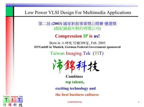
<strong>Low</strong> <strong>Power</strong> <strong>VLSI</strong> <strong>Design</strong> <strong>For</strong> <strong>Multimedia</strong> <strong>Applications</strong><br />
第二屆 (2003) 國家新創事業獎公開賽 優選獎<br />
(創紀錄最年輕的得獎公司)<br />
<strong>Compression</strong> IP is us!<br />
Born in 工研院 52館308室, Feb. 2003<br />
IITGmbH in Munich, German Federal Government sponsored<br />
Taiwan Imaging Tek (TIT)<br />
Combines<br />
top talents,<br />
exciting technology and<br />
the best business cultures<br />
CONFIDENTIAL 1
T<br />
I T<br />
Historical Moment (29-10-03, 27-05-01)<br />
優選獎 winner, 10-2003<br />
among 193 companies 2003<br />
TOP 10 winner (among 257 teams)<br />
in MBPW 2001, Munich, Germany<br />
沛錦科技願景 - 快樂 創新 的 研發 團隊,踏實 守紀 的追求效益<br />
CONFIDENTIAL 2
T<br />
I T<br />
美國<br />
綠色矽島<br />
台<br />
灣<br />
Pioneer of A-V IP business<br />
德國<br />
產、官、學、研<br />
+ 國際合作<br />
致力台灣 科技 質與量 的 躍昇<br />
謹將慈愛、萬能的 上帝<br />
恩賜給沛錦的一切<br />
獻給我們熱愛的祖國!<br />
Royalty Fee<br />
Royalty<br />
沛錦<br />
The Dream Is Alive! (NASA Museum 3D Movie Title)<br />
CONFIDENTIAL 3<br />
Fee
T<br />
I T<br />
<strong>Low</strong> <strong>Power</strong> <strong>VLSI</strong> <strong>Design</strong> for Visual Communications<br />
� <strong>Power</strong> saving from system, algorithm and architecture<br />
� Principle of low power <strong>VLSI</strong> design<br />
� Logic gate<br />
� Circuit<br />
� Application specific <strong>VLSI</strong> Cell library<br />
� <strong>Low</strong> power memory design (DRAM, SRAM, ROM, NVM)<br />
� <strong>Low</strong> power analog circuit (Ex. Sense/Op amp)<br />
� Application specific designs<br />
� Locality<br />
� Stand-by mode<br />
� Device/Process<br />
� <strong>Low</strong> power process with low power cells<br />
� <strong>Design</strong> tradeoffs (Examples: Data Path, CPU)<br />
Reference:<br />
1. Gary K. Yeap “Practical <strong>Low</strong> <strong>Power</strong> Digital <strong>VLSI</strong> <strong>Design</strong>” by Kap, 1998<br />
2. Dr. SY Huang, NTHU (Dr.黃錫瑜, 清華 U)<br />
3. K. Roy, S. Prasad “<strong>Low</strong>-<strong>Power</strong> CMOS <strong>VLSI</strong> Circuit <strong>Design</strong>”<br />
4. “<strong>VLSI</strong> Memory Chip <strong>Design</strong>”<br />
CONFIDENTIAL 4
T<br />
I T<br />
Hierarchical <strong>Low</strong> <strong>Power</strong> <strong>VLSI</strong> <strong>Design</strong><br />
System<br />
Algorithm<br />
Architecture<br />
Circuit/Logic<br />
Layout<br />
Process<br />
<strong>Power</strong> budgeting, component selection, S/W vs. H/W<br />
block partitioning, power management<br />
Algorithm, data transformation, supply voltage scheduling,<br />
data representation, application specific<br />
Parallelism, pipelining, re-timing, adaptive voltage scaling,<br />
optimal choice of data representation, optimization of signal<br />
ordering, minimization of glitch/noise, optimal resource<br />
allocation<br />
Re-sizing, logic style, parallelism, MTCMOS, VTCMOS,MSV,<br />
DGCMOS, power management, stand-by<br />
<strong>Power</strong> driven P&R, low power layout, low power cell library<br />
<strong>Low</strong> powered device, Extended technologies (with special cell lib<br />
incl: MTCMOS, VTCMOS, DGCMOS, MSV ), alternative<br />
technology (SOI, SOIAS…)<br />
(Modified from TUM, Tech. Univ. Munich)<br />
CONFIDENTIAL 5
T<br />
I T<br />
Software<br />
Hardware<br />
Software vs. Hardware<br />
Advantage Disadvantage<br />
�Seems to be free<br />
�High flexibility<br />
�Ease of compatibility<br />
�High speed<br />
�<strong>Low</strong> power<br />
�High efficiency<br />
� Hardware solution:<br />
�High power consumption<br />
�Slow in execution<br />
�Inefficient<br />
�High die cost<br />
�Less flexibility<br />
�<strong>Low</strong> compatibility<br />
Rule of Work partitioning<br />
� Computing power hunger: ME/MC, DCT, VLC<br />
� Fixed and routine calculation<br />
� Software solution:<br />
� Misc.<br />
� Packing, data parsing,<br />
A-V synchronization<br />
CONFIDENTIAL 6
T<br />
I T<br />
Data <strong>Compression</strong> Algorithms to Save Data & <strong>Power</strong><br />
PC /<br />
Internet<br />
Good algorithm achieves:<br />
High performance<br />
<strong>Low</strong> cost<br />
<strong>Low</strong> <strong>Power</strong><br />
US patent pending<br />
U-Controller<br />
(Ex. 8051)<br />
SM1 SM2 . . . SMn<br />
Data Path ROM/SRAM<br />
VLC<br />
沛錦 IP<br />
Flash<br />
Memory<br />
ImagingTek<br />
<strong>Compression</strong><br />
Codec<br />
CONFIDENTIAL 7
T<br />
I T<br />
<strong>Low</strong> <strong>Power</strong> CPU and Caching System (1)<br />
� Instruction hit rate vs. ration between Register and L1/L2cache<br />
� Application dependent!<br />
� Hit rate vs. the cache size and instruction allocation<br />
� Access and storage of the most frequently used instructions (M.E.,<br />
DCT, VLC)<br />
� Probability of the most recent accessed instruction<br />
� Continuous instruction and data access by Column Switching<br />
. . .<br />
Thumb of rule: Avoid accessing larger cache/buffer<br />
CPU<br />
Reg.<br />
Reg.<br />
Reg.<br />
L1<br />
Cache<br />
L2<br />
Cache<br />
Off-Chip<br />
Memory<br />
CONFIDENTIAL 8
T<br />
I T<br />
<strong>Power</strong> Management Mode<br />
� Example: <strong>Power</strong>PC 603<br />
Mode 80 MHz<br />
No power management 2.54 W<br />
Dynamic power management 2.20 W<br />
DONE 366 mW<br />
NAP 135 mW<br />
SLEEP 105 mW<br />
SLEEP without PLL 19 mW<br />
SLEEP without system clock 2 mW<br />
CONFIDENTIAL 9
T<br />
I T<br />
Principle of <strong>Low</strong> <strong>Power</strong> <strong>VLSI</strong> <strong>Design</strong><br />
� Reducing the power supplier level<br />
� Using lowest frequency of Clocks<br />
� Minimizing the geometry<br />
� Minimizing the switching activities<br />
� Applying parallel and/or pipelining design to lower<br />
requirement frequency of operation<br />
� Removing redundant buffer/loadings and<br />
operations (SoC)<br />
CONFIDENTIAL 10
T<br />
I T<br />
Performance management(1):Multiple CLKs<br />
Multiple clocking schemes: each driving circuit of different<br />
performance requirement<br />
66 MHz<br />
Cache<br />
Memory 1<br />
Cache<br />
Memory 2<br />
133 MHz<br />
JPEG/DCT<br />
50 MHz<br />
100 MHz<br />
System<br />
Controller<br />
(8051/ARM7)<br />
200 MHz<br />
Motion<br />
Estimator<br />
Frame<br />
Buffer<br />
Buffer<br />
10 MHz<br />
20 MHz<br />
CONFIDENTIAL 11
T<br />
I T<br />
Performance management (1):Multiple VDDs<br />
Multiple voltage schemes: each driving circuit of different<br />
performance requirement<br />
3.0V<br />
Cache<br />
Memory 1<br />
Cache<br />
Memory 2<br />
133 MHz<br />
JPEG/DCT<br />
2.7V<br />
2.5V<br />
System<br />
Controller<br />
(8051/ARM7)<br />
3.3V<br />
Motion<br />
Estimator<br />
Buffer<br />
2.0V<br />
Frame<br />
Buffer<br />
1.5V<br />
CONFIDENTIAL 12
T<br />
I T<br />
Performance management (Continued)<br />
Boost supply voltage in critical path<br />
DC Voltage controller/regulator (US patent pending)<br />
Data In<br />
Clock<br />
Critical<br />
timing<br />
info<br />
VCC Level<br />
Controller<br />
Regulator<br />
Target Block<br />
300 MHz<br />
Data Out<br />
Break 1<br />
CONFIDENTIAL 13
T<br />
I T<br />
Instruction<br />
Fetch<br />
.<br />
.<br />
.<br />
.<br />
Switching Activity Management<br />
Avoid unnecessary switching!<br />
Ex. Mux the input to multiplier and ALU<br />
ALU_Enable<br />
ALU Multiplier<br />
Multiplier_Enable<br />
DA[0:15]<br />
DB[0:15]<br />
CONFIDENTIAL 14
T<br />
I T<br />
Switching Activity Management (Continue)<br />
Wide width CPU/ALU/Data Path/Multiplier…<br />
� Mask out some nonfunctioning bits<br />
� Both HW or SW solution work<br />
8-bit<br />
CPU<br />
8-bit<br />
CPU<br />
8-bit<br />
CPU<br />
8-bit<br />
CPU<br />
O-Bus<br />
X-Bus<br />
Y-Bus<br />
Chip<br />
Select<br />
Chip<br />
Select<br />
Chip<br />
Select<br />
Chip<br />
Select<br />
CONFIDENTIAL 15
T<br />
I T<br />
Switching Activity Management (Continue)<br />
Bus sharing (long bus load)<br />
� With timing or phase control<br />
� Min. coupling noise effect<br />
� Min. switching activities<br />
� Min. area<br />
s1 D1<br />
s2 D2<br />
Separate data bus<br />
s1 D1<br />
s2 D2<br />
Shared data bus<br />
CONFIDENTIAL 16
T<br />
I T<br />
Switching Activity Management (Continue)<br />
Reducing long load<br />
� By removing the redundant load<br />
1 1<br />
A[0:15] B[0:15]<br />
FA<br />
1’s complement [0:15]<br />
1’s complement<br />
1 1<br />
A[0:15] B[0:15]<br />
FA [0:15]<br />
CONFIDENTIAL 17
T<br />
I T<br />
CLK:1/3 f<br />
<strong>Low</strong>er Supply Voltage: Pipelined architecture<br />
CLK: f<br />
Function 1<br />
Function<br />
Function 2<br />
3 pipes of sub-function: cut down the frequency and supply voltage level<br />
Function3<br />
CONFIDENTIAL 18
T<br />
I T<br />
<strong>Low</strong>er Supply Voltage: Parallel Architecture<br />
Trade VCC with lower clock rate<br />
to achieve the same output throughput<br />
Input Output<br />
Processor<br />
CL=C<br />
VCC=V<br />
Freq.=f<br />
f<br />
Input<br />
CL=2.2C<br />
VCC=0.6V<br />
Freq.=0.5f<br />
Processor<br />
f / 2<br />
Processor<br />
f / 2<br />
Output<br />
CONFIDENTIAL 19
T<br />
I T<br />
<strong>Low</strong> <strong>Power</strong> Profit (From the Gap)<br />
<strong>Low</strong> <strong>Power</strong><br />
SoC<br />
Limitation<br />
Logic<br />
(CPU)<br />
Memory<br />
<strong>Low</strong> <strong>Power</strong> <strong>Multimedia</strong> System:<br />
Trade logic with memory<br />
MPEG vs. JPEG<br />
MPEG 1 vs. MPEG 4<br />
MP3 vs. AAC (audio)<br />
IO<br />
<strong>Power</strong><br />
Technology migration trend<br />
CONFIDENTIAL 20
T<br />
I T<br />
Reduce Operation: Length Reduction<br />
Operand selection: Take advantage of the correlation between<br />
pixels. Calculate only a certain length of the LSB bits<br />
Benefit:<br />
� Performance enhancement<br />
� Reduce power consumption<br />
164 162 162 162 162 163 163 164<br />
163 161 159 162 167 164 165 163<br />
164 163 163 161 159 156 159 160<br />
163 158 152 152 153 155 153 156<br />
154 153 152 151 150 149 148 149<br />
149 151 150 150 151 152 150 149<br />
147 146 148 151 149 150 148 149<br />
148 149 148 148 147 147 146 146<br />
A sub-Claim of<br />
an US patent in<br />
M.E. & DCT<br />
CONFIDENTIAL 21
T<br />
I T<br />
Reduce Operation: Simple Operator<br />
Take advantage of the smaller gate of circuit<br />
Ex1. Y = AB + AC � Y = A * (B + C)<br />
Ex2. Y = 7X � Y = (X
T<br />
I T<br />
Noise<br />
� Where the noise come from?<br />
� Inductance effect (from current flow, L(di/dt) )<br />
� Supply noise: <strong>Power</strong> and ground bouncing<br />
� Coupling noise<br />
� Others:<br />
� Alpha particle (Dangerous to DRAM)<br />
� External noise sources<br />
� Thermal noise (sensitivity high circuit)<br />
� Solution of noise reduction<br />
� Avoid simultaneously switching: distributed timing<br />
� Keep sensitive circuits away from noise source<br />
� Substrate coupling: guard ring, moving away the source<br />
� Noise elimination circuits: Cap, RC, circuits …<br />
CONFIDENTIAL 23
T<br />
I T<br />
<strong>Low</strong> <strong>Power</strong> Layout<br />
How layout can minimize the power consumption<br />
� Small Diffusion area (output node) in layout<br />
� Use upper layer connecting material (M6,M5… than M1)<br />
� Distance from coupling signal<br />
� Minimized input gate size (W_min.)<br />
Co<br />
Cc<br />
Cg<br />
CL = Co + Cc + Cg<br />
CONFIDENTIAL 24
T<br />
I T<br />
<strong>Low</strong> <strong>Power</strong> Memory <strong>Design</strong> (Continue)<br />
.<br />
.<br />
The Diagram of a Memory Block<br />
Row<br />
Decoder<br />
Word<br />
Line<br />
Driver<br />
Sense Amplifier<br />
Column Decoder<br />
Cell<br />
SA<br />
CONFIDENTIAL 25
T<br />
I T<br />
<strong>Low</strong> <strong>Power</strong> Memory <strong>Design</strong>(Continue)<br />
� Most power consuming circuit:<br />
� Word line driver<br />
� Sense amplifier<br />
� Pre-charging<br />
� Scalable word line driver: depends on the load capacitance<br />
� Scalable sense amplifier: current source vs. gain<br />
� Multiple bank of memory arrays (cost. <strong>Applications</strong>…): small<br />
cap. Load, low power waste<br />
� Continuous data accessing: from column switching<br />
CONFIDENTIAL 26
Pre-charge<br />
T<br />
WL<br />
CBL<br />
I T<br />
<strong>Low</strong> <strong>Power</strong> Memory <strong>Design</strong>(Continue)<br />
Pre-charging scheme<br />
� <strong>For</strong> performance and cell size consideration, most memories<br />
Ex. SRAM<br />
pre-charge BL and BL to Vcc<br />
SA<br />
BL<br />
CBL<br />
CLK<br />
WL<br />
Pre-charge<br />
BL vs. BL-Bar<br />
SA_Enable<br />
Data Out<br />
CONFIDENTIAL 27
T<br />
I T<br />
� Ground the BL and BL!! Why?<br />
ImagingTek’s Sensing Scheme<br />
� Clean Ground! Discharge<br />
faster thru NMOS<br />
� Slow pull-up by PMOS<br />
� Less noise!<br />
� Allow more time for access<br />
� Allow less input<br />
differential voltage<br />
� <strong>Low</strong> power<br />
� Non-overlapping<br />
between WL and<br />
discharging<br />
(US patent<br />
pending)<br />
D<br />
WL Disable<br />
31<br />
36 37<br />
Self-timer<br />
39<br />
BL<br />
BL<br />
CONFIDENTIAL 28<br />
33<br />
SA<br />
331<br />
35<br />
38<br />
34<br />
32
T<br />
I T<br />
void Glitch And Overlapping In Memory<br />
� Glitch might turn on memory cell (SRAM/ROM even severe)<br />
� Overlapping during word line transition<br />
� Overlapping of Word line and pre-charging<br />
� Word line glitch causes power consumption within cell<br />
Decoder<br />
M-Cell<br />
M-Cell<br />
X 1000<br />
CONFIDENTIAL 29
T<br />
I T<br />
� Architecture: Multiple banks<br />
<strong>Low</strong> <strong>Power</strong> DRAM<br />
� Self stand-by mode: Refreshing only<br />
those banks with valuable data<br />
� Longer refreshing duration: Reducing<br />
the leaking current<br />
� Leaking current<br />
� Sub-threshold current<br />
� Tradeoff between Vdd and Vt<br />
I_ stand-by = I_leak + I_sub-threshold<br />
P+<br />
BL<br />
WL<br />
I_S<br />
N+ N+<br />
Reversely<br />
biased<br />
I_L<br />
Deep<br />
Drench<br />
Capacitor<br />
CONFIDENTIAL 30<br />
-<br />
-<br />
-<br />
-<br />
-<br />
-<br />
-<br />
-<br />
P- well or<br />
substrate
T<br />
I T<br />
Principle of the NMV<br />
� Vt difference to identify the “programmed” and “Erased”<br />
bits.<br />
� V_WL/VCC can turn on the erased cell,<br />
� V_WL/VCC can not turn on the programmed cell.<br />
How to change the Vt<br />
� Programming (Vt=VCC+2V): Hot electron injection<br />
� Erasing (Vt=VCC-1V): Electron tunneling<br />
Vpp<br />
e-<br />
E<br />
Vpp/Vcc<br />
N+ N+<br />
CONFIDENTIAL 31<br />
e
T<br />
I T<br />
Vt<br />
Vg= -12V, ..<br />
-8V<br />
Erasing Time<br />
(Log function)<br />
Timing vs. HV Levels<br />
X-, Y- scale are<br />
log function<br />
Vs=12V, ..<br />
8V<br />
Vt<br />
Vg=<br />
Programming Time<br />
(Log function)<br />
12V<br />
11V<br />
10V<br />
9V<br />
CONFIDENTIAL 32
T<br />
I T<br />
Issues in NVM<br />
� High voltages cause risk of junction breakdown in G,D,S<br />
� Programmed and erased bit voltage margin vs. reprogrammable<br />
cycle times<br />
� Over erase: Vt shift to cause leakage of erases bits(and<br />
circuit failure in reading), might cause failure in reading<br />
� Circuits can minimize the risk: reduced E<br />
WL<br />
Defect<br />
Erased Programmed<br />
0V 2V VCC 5V<br />
Normal<br />
WL<br />
Erased Programmed<br />
0V 2V VCC 5V<br />
CONFIDENTIAL 33
T<br />
I T<br />
Principle of the <strong>Low</strong> <strong>Power</strong> NVM<br />
Consumes high power during programming and erasing<br />
How to achieve low power?<br />
� Reduce the 3 factors: CL, Vcc/Vpp, Time<br />
� <strong>Low</strong> voltage in Source, Gate and Drain!<br />
� Shorter time of circuit ON!<br />
� Smaller device<br />
� Future trends:<br />
� New NVM ( > year 2006)<br />
Application specific!!!<br />
CONFIDENTIAL 34
T<br />
I T<br />
<strong>Low</strong> <strong>Power</strong> Bus<br />
Conventional: Bus voltage swings from Vdd to Gnd<br />
<strong>Low</strong> power bus<br />
� <strong>Low</strong> voltage swing (similar to the USB bus)<br />
Driver<br />
V_bus<br />
V_ref (optional depends on<br />
speed requirement)<br />
“1”<br />
“0”<br />
V_bus<br />
CB<br />
(+/- 100mV swing)<br />
Receiver<br />
V_ref<br />
CONFIDENTIAL 35
T<br />
I T<br />
Charge Recycling<br />
Energy saving approaches: no discharge if possible<br />
� Charge on higher order data bit moves to lower data bit<br />
� Charge in one circuit moves to another<br />
� Charge flows from one node to another<br />
� One circuit, multiple function<br />
Ex. 1. From B15 discharge to B13<br />
Ex. 2. From a charge pump to a sense amplifier<br />
Ex. 3. From a node moves to another<br />
Ex. 4. From one level changes to another<br />
CONFIDENTIAL 36
T<br />
I T<br />
Charge recycling from Charge Pump to S.A.<br />
A charge pump with output level of 12V and load of 5pF<br />
� These charge can be used to be the supply of a sense amplifier<br />
� Can be used to charge another charge pump<br />
12 V charge pump<br />
1<br />
2<br />
1 1<br />
2 1<br />
. . .<br />
Regulator<br />
Vo<br />
5 pF<br />
V+<br />
V-<br />
S.A.<br />
<strong>Power</strong><br />
Supply<br />
CONFIDENTIAL 37
T<br />
I T<br />
� Select the right one!<br />
Storage Devices<br />
Latch and Flip-Flop<br />
� In general: a Flip-Flop requires 2X gate/area than a latch<br />
� In HDL coding: understand the coding style and the<br />
synthesis tool’s capability<br />
� Each of the latch and FF is tradeoff among setup time, hold<br />
time, clocking design complexity, time delay. . .<br />
� Key different between latch and Flip-Flop: Latch has ONE<br />
stage and FF has 2 stages (Master-Slave) of storage<br />
CONFIDENTIAL 38
T<br />
D<br />
I T<br />
<strong>Low</strong> power<br />
Q<br />
<strong>Low</strong> <strong>Power</strong> Flip-Flop<br />
Q<br />
CLK<br />
D<br />
CONFIDENTIAL 39<br />
D<br />
High gain, High speed, <strong>Low</strong> power<br />
Q<br />
Q
T<br />
I T<br />
Tradeoff Between Gain And Speed<br />
Reducing the current source level still keeps<br />
good speed, but reduce power consumption<br />
� Gain is proportional to the inverse square of the biased current:<br />
Av ~ 1 / I_Bias<br />
� Speed is linearly proportional to the bias current<br />
BW ~ I_Bias<br />
� Performance is proportional to the product of Gain and BW<br />
Av<br />
A1<br />
A2<br />
Area1 = Area2<br />
CONFIDENTIAL 40<br />
f
T<br />
I T<br />
High Speed Sensing Amplifier<br />
� Breaking a high gain stage into multiple low gain stages<br />
� Optimizing the current load ration of the current sources<br />
� Trade performance for low power<br />
SA SA SA1 SA SA2<br />
Av=100<br />
I-cs= 50 uA<br />
Av1 = Av2 = 10<br />
I-cs1= 5 uA, I-cs2= 15 uA<br />
CONFIDENTIAL 41
T<br />
I T<br />
SoC and the Benefit in <strong>Low</strong> <strong>Power</strong><br />
Why SoC<br />
Semiconductor process migration trend: cost down<br />
� Benefit: lower cost of<br />
� Die<br />
� Packaging<br />
� Testing<br />
� <strong>Low</strong> power from SoC<br />
� Removing redundant buffer<br />
� Remove redundant operation<br />
� Remove I/O pad load capacitor<br />
CONFIDENTIAL 42
T<br />
I T<br />
Stand-By Mode in Transceiver<br />
Principle: (similar to ) One way Tx / Rx<br />
Why wasting power if no voice to be sent?<br />
� Standby mode + detection<br />
� Multiple stages driver<br />
� Parallelism (US patent pending)<br />
Voice<br />
detector<br />
Stand-By<br />
SA<br />
Signal processing<br />
SA1 SA SA2 . . .<br />
SA<br />
PA<br />
CONFIDENTIAL 43
T<br />
I T<br />
MTCMOS: Multiple Threshold CMOS Devices<br />
Stand-by<br />
Stand-by<br />
Hi Vt<br />
CMOS Logic<br />
With low Vt<br />
Hi Vt<br />
<strong>Low</strong> Vt<br />
� Two kinds of devices in cut<br />
down the stand-by current<br />
� <strong>Low</strong> Vt: operating mode<br />
� High Vt: Stand-by mode<br />
(lower leakage)<br />
CONFIDENTIAL 44
T<br />
I T<br />
VTCMOS: Variable-Threshold Circuits: Back Biasing<br />
� <strong>Low</strong> power principle: low Vdd (along with) low Vt<br />
� Problem: higher sub-threshold current<br />
� Solution: Adjust Vt during stand-by mode: back biasing<br />
� Twin well process<br />
VBP: 2V (active)<br />
4V (stand-by)<br />
VBN: 0V (active)<br />
-2V (stand-by)<br />
2 Substrate<br />
Bias Circuits<br />
CONFIDENTIAL 45
T<br />
I T<br />
<strong>Low</strong> <strong>Power</strong> <strong>VLSI</strong> for Visual Communication<br />
Rule: Algorithm! Algorithm! Algorithm! + Tradeoffs<br />
� SoC: Compressing the Frame Buffer!<br />
� Fast DCT<br />
� Fast ME: Accurate starting point prediction<br />
� Scalable searching range<br />
� Stop buffer clock during DCT, M.E.<br />
� Hi-speed pixel bus<br />
� LSBs and sub-sampling calculations<br />
� Performance (Vdd, Freq.) management<br />
CONFIDENTIAL 46
T<br />
I T<br />
<strong>Low</strong> <strong>Power</strong> Communication System<br />
Cut down the power in critical devices<br />
� <strong>Low</strong> stand-by current<br />
� <strong>Low</strong> power display<br />
� <strong>Low</strong> power level: less bright<br />
� Interleaving mode<br />
� <strong>Low</strong> power transceiver<br />
� Reducing the switching activity<br />
CONFIDENTIAL 47
T<br />
I T<br />
<strong>Low</strong> <strong>Power</strong> Data Path With Timing Control<br />
PM<br />
T Machine<br />
Flow<br />
Control<br />
8x8/16x16 Buffer<br />
+-
T<br />
I T<br />
ImagingTek’s <strong>Low</strong> <strong>Power</strong> DCT: world fastest DCT<br />
Means Add Multiply Shift<br />
Gate<br />
Switch<br />
Rate<br />
Eq. 4000 9200 256 150X<br />
Fast<br />
DCT<br />
Integer<br />
DCT<br />
464 192 0 1X<br />
(REF.)<br />
466 96 0 4X<br />
TIT1
T<br />
I T<br />
Frame Buffer <strong>Compression</strong>!<br />
MPEG<br />
V-encoder<br />
Previous<br />
Frame<br />
Off-chip<br />
Next<br />
Frame<br />
US patent<br />
PF<br />
MPEG<br />
V-encoder<br />
Lossless Codec<br />
NF<br />
Single Chip<br />
US Patent<br />
pending<br />
CONFIDENTIAL 50
T<br />
I T<br />
M.E. Scalable Searching Range<br />
MV=<br />
(0,0)<br />
52<br />
MV=<br />
(6,0)<br />
53<br />
MV=<br />
(0,6)<br />
51<br />
54<br />
US patent<br />
pending<br />
MV=<br />
(3,0)<br />
CONFIDENTIAL 51<br />
55
T<br />
I T<br />
TIT’s MPEG Performance Enhancement (1)<br />
Motion<br />
Estimation<br />
17% 10 13%<br />
6 5 13<br />
MC+DCT+Q+<br />
VLC+Packing<br />
55% 32% 13%<br />
SW / FW solution (>2.5X speedup)<br />
ImagingTek<br />
FW + ASIC solution (>4X speedup)<br />
Others<br />
CONFIDENTIAL 52
T<br />
I T<br />
ImagingTek ASIC solution for MPEG/JPEG<br />
World fastest V-core with<br />
lowest power consumption<br />
(
T<br />
I T<br />
Summary<br />
� Principle: Never over design!<br />
Algorithm + Architecture + Circuit + Memory<br />
� System Spec. power budget, floor plan (VDD/GNG)<br />
� Software vs. Hardware partitioning<br />
� Caching system<br />
� Algorithm + <strong>VLSI</strong> architecture<br />
� Performance management (Vdd, f)<br />
� Switching activity minimization<br />
� Memory (architecture + circuit)<br />
� Cell selection<br />
� Noise, glitch minimization<br />
� Charge recycling<br />
� Analog: Av ��BW trade off<br />
� Standby current reduction<br />
� <strong>Low</strong> <strong>Power</strong> <strong>VLSI</strong> design for <strong>Multimedia</strong> applications<br />
CONFIDENTIAL 54
T<br />
I T<br />
CAD for <strong>Low</strong> <strong>Power</strong> <strong>VLSI</strong> <strong>Design</strong> (1)<br />
Business opportunity<br />
� Industry is crying for low power tools<br />
CAD company<br />
� Automatic (or semi-automatic) optimizing the <strong>VLSI</strong><br />
� Pre-design design guidelines (rules)<br />
Service company<br />
� <strong>Low</strong> power optimization service<br />
� <strong>Low</strong> power cell library<br />
CONFIDENTIAL 55
T<br />
I T<br />
CAD for <strong>Low</strong> <strong>Power</strong> <strong>VLSI</strong> <strong>Design</strong> (2)<br />
� Circuit<br />
� Logic<br />
Automatically Optimization Tool<br />
� <strong>Low</strong> CL<br />
� <strong>Low</strong> leakage, low noise, low glitch<br />
� Reducing switching activities<br />
� Optimization HDL coding<br />
� Memory<br />
� CPU<br />
� Scalability<br />
� Bank re-ordering<br />
� Caching<br />
� <strong>Power</strong> management instruction<br />
CONFIDENTIAL 56
T<br />
I T<br />
CAD for <strong>Low</strong> <strong>Power</strong> <strong>VLSI</strong> <strong>Design</strong> (3)<br />
� Architecture:<br />
� stand-by mode<br />
� Minimizing redundant circuit (SoC or …)<br />
� Algorithm transformations<br />
� <strong>Low</strong> power algorithm selection<br />
� DWT to DCT<br />
� MP3�MP2<br />
� ADPCM-DPCM<br />
� Application specific:<br />
� Flash (memories)<br />
� LCD<br />
� Image sensors, …<br />
CONFIDENTIAL 57
T<br />
I T<br />
CAD for <strong>Low</strong> <strong>Power</strong> <strong>VLSI</strong> <strong>Design</strong> (4)<br />
� Steps<br />
� 80-20 theory !!<br />
� Resources<br />
� NSC supported projects<br />
� Industry’s need<br />
� SIG: Special Interest Group<br />
� IP Mall<br />
CONFIDENTIAL 58