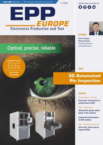
EPP Europe P1.2019
- Text
- Qualitaetssicherung
- Schablonendruck
- Loetprozess
- Leiterplattenfertigung
- Baugruppenfertigung
- Zukunftstechnologien
COVER Capabilities and
COVER Capabilities and limitations of AXI and 3D AOI I 4.0 for inspection in the electronics industry In a connected smart factory, all machines and systems essentially become smart sensors, collecting all possible data from the production line and the boards themselves. It is obvious that the quality of the raw data is one of the core components. Therefore, the accuracy and sensitivity of those sensors is very critical, especially in quality control systems such as AOI and AXI. Without diminishing the strong characteristics of the in-line inspection equipment, these still need assistive technologies for the verification of some challenging faults that appear at the same pace as the miniaturization of electronic assemblies. Ragnar Vaga, Yxlon International GmbH, Germany 38 EPP EUROPE April 2019
COVER In recent years, Package on Package (POP) and Bottom Termination Components (BTCs) devices have become very important and widely used in the PCBA manufacturing process. Two of the most challenging PCBA process failures are component warpage and HoP defects. Therefore, achieving the best possible solder joint quality becomes an increasingly important consideration for the PCB assemblers. Most of the solder joints of a POP and BTC device are invisible by optical means, so X-ray inspection is the only way to examine the solder quality in a non-destructive way. At the same time, the only method for assessing the warpage and co-planarity issues of the component is 3D AOI. As a consequence, AXI and 3D AOI are more frequently used on the SMT lines. However, both these technologies have certain limitations that may need assistive technologies for the verification of possible false faults. The false-fault rate of the inspection system, one of the key items of the fault coverage, affects the overall efficiency of defect detection. Simply put, the more false faults you pass on to a repair station for validation, the more real defects could get missed. False faults generate costs. Each defect reported by AOI or AXI must be verified. If the reported defect turns out to be a false alarm, then its verification effort is a cost that could have been saved, because the verification did not create any real value. False-alarm verification costs include labor, capital equipment and other related costs such as factory overheads and panel handling. Due to the continuous miniaturization of SMT components and increasing complexity of the assemblies, false faults have not been eliminated so far and smart verification strategies should be implemented. Component warpage and Head on Pillow (HoP) Component warpage: For PoP packages, the warpage issue is always one of the most difficult for SMT process engineers, because it is easy to cause an open solder joint problem. The typical SMT defect modes, such as non-wet open, solder bridging, head and pillow, and noncontact open are applicable to both the joints between the PoP bottom package with the board and the PoP memory package. Package warpage is widely recognized as a primary factor in the formation of HoP. In fact, several industry consortia efforts are currently in progress to help characterize factors influencing package warpage behavior in an attempt to define mitigation measures. These include the iNEMI Package Warpage Qualification Criteria and the HDPUG FCBGA Package Warpage projects. Source: Yxlon Due to the continuous miniaturization of SMT components and increasing complexity of the assemblies, false faults have not been eliminated so far and smart verification strategies should be implemented. EPP EUROPE April 2019 39
- Page 1: 04 2019 www.epp-europe.eu INTERVIEW
- Page 4 and 5: Contents 04 2019 European Magazine
- Page 6 and 7: NEWS + HIGHLIGHTS Removing siloed e
- Page 8 and 9: NEWS + HIGHLIGHTS The Europe Direct
- Page 10 and 11: NEWS + HIGHLIGHTS Adapting towards
- Page 12 and 13: NEWS + HIGHLIGHTS First roadmap to
- Page 14 and 15: NEWS + HIGHLIGHTS Global sales dire
- Page 16 and 17: NEWS + HIGHLIGHTS Source: EMA Desig
- Page 18 and 19: TRADE SHOWS + EVENTS Source: Mesago
- Page 20 and 21: TRADE SHOWS + EVENTS IPC Apex Expo
- Page 22 and 23: TRADE SHOWS + EVENTS A handful of e
- Page 24 and 25: TRADE SHOWS + EVENTS The future of
- Page 26 and 27: TRADE SHOWS + EVENTS 1. LED meets S
- Page 28 and 29: TRADE SHOWS + EVENTS Christian Koen
- Page 30 and 31: TRADE SHOWS + EVENTS Source: EPP Eu
- Page 32 and 33: TRADE SHOWS + EVENTS The future of
- Page 34 and 35: TRADE SHOWS + EVENTS Fuji Innovatio
- Page 36 and 37: TRADE SHOWS + EVENTS A demonstratio
- Page 40 and 41: COVER Typical SMT defect modes. Sou
- Page 42 and 43: COVER Source: Yxlon Head on Pillow
- Page 44 and 45: PCB + ASSEMBLY EMS provider with a
- Page 46 and 47: PCB + ASSEMBLY PRODUCT UPDATES Mate
- Page 48 and 49: PCB + ASSEMBLY Helping with continu
- Page 50 and 51: PCB + ASSEMBLY ADAS take advantage
- Page 52 and 53: PCB + ASSEMBLY Source: Indium Sourc
- Page 54 and 55: PCB + ASSEMBLY Source: Indium For t
- Page 56 and 57: PCB + ASSEMBLY Circuit boards immer
- Page 58 and 59: PCB + ASSEMBLY PRODUCT UPDATES PCB
- Page 60 and 61: PCB + ASSEMBLY Process tracking and
- Page 62 and 63: PCB + ASSEMBLY PRODUCT UPDATES Incr
- Page 64 and 65: PCB + ASSEMBLY Sensing the world’
- Page 66 and 67: PCB + ASSEMBLY PRODUCT UPDATES Syst
- Page 68 and 69: PCB + ASSEMBLY Reliable protection
- Page 70 and 71: PCB + ASSEMBLY Example of a tempera
- Page 72 and 73: PCB + ASSEMBLY At the heart of prod
- Page 74 and 75: PCB + ASSEMBLY PRODUCT UPDATES UV c
- Page 76 and 77: PCB + ASSEMBLY Encapsulation optimi
- Page 78 and 79: PCB + ASSEMBLY Alistair Little is t
- Page 80 and 81: PCB + ASSEMBLY PRODUCT UPDATES Flex
- Page 82 and 83: TEST + QUALITY ASSURANCE Timely fau
- Page 84 and 85: TEST + QUALITY ASSURANCE Accelerate
- Page 86 and 87: TEST + QUALITY ASSURANCE Fatigue fr
- Page 88 and 89:
TEST + QUALITY ASSURANCE PRODUCT UP
- Page 90 and 91:
ADVERTISERS Advertisers / Editorial
Inappropriate
Loading...
Mail this publication
Loading...
Embed
Loading...


