Unbalancer 9-pin.pdf - Tube CAD Journal
Unbalancer 9-pin.pdf - Tube CAD Journal
Unbalancer 9-pin.pdf - Tube CAD Journal

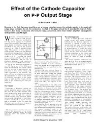
Create successful ePaper yourself
Turn your PDF publications into a flip-book with our unique Google optimized e-Paper software.
GlassWareAUDIO DESIGNUSER GUIDEIntroductionOverviewSchematicsRecommended ConfigurationsAssembly InstructionsGlassWareAUDIO DESIGNwww.glass-ware.comwww.tubecad.comsales@glass-ware.comCopyright © 2011All Rights Reserved03/15/2011
DANGER!This PCB holds a high-voltage power supply; thus, a real—and possibly—lethal shock hazard exists.Ideally, a variac should be used to slowly power up theregulator, as it is better to have a mis-oriented electrolyticcapacitor or a mis-located resistor blow at low voltages,rather than at high voltages. Remember that the dangerincreases by the square of the voltage; for example, 200volts is four times more dangerous than 100 volts and 400volts is sixteen times more dangerous.Once the power supply is powered up, be cautious at alltimes. In fact, even when the power supply is disconnectedor shut down, assume that power-supply capacitors will haveretained their charge and, thus, can still shock. If you are notan experienced electrical practitioner, before attaching thetransformer windings to the board, have someone who iswell-experienced in electronics review your work.There are too few tube-loving solder slingers left; we cannotafford to lose any more.GlassWareAUDIO DESIGNwww.glass-ware.comwww.tubecad.comsales@glass-ware.comCopyright © 2011All Rights Reserved
GlassWare Audio DesignWarning!This PCB contains a high-voltage power supply; thus, a real and lethal shock hazardexists. Once the power transformer is attached, be cautious at all times. In fact, alwaysassume that the high voltage capacitors will have retained their charge even after thepower supply has been disconnected or shut down. If you are not an experiencedelectrical practitioner, before applying the AC voltage have someone who isexperienced review your work. There are too few tube-loving solder slingers left; wecannot afford to lose any more.OverviewThank you for your purchase of the <strong>Unbalancer</strong> 9-<strong>pin</strong> stereo PCB. This FR-4PCB is extra thick, 0.094 inches (inserting and pulling tubes from their sockets won’tbend or break this board), double-sided, with plated-through heavy 2oz copper traces.In addition, the PCB is lovingly and expensively made in the USA. The boards are 7by 6 inches, with five mounting holes, which helps to prevent excessive PCB bendingwhile inserting and pulling tubes from their sockets.Each PCB holds two differential line-stage amplifiers, each followed by aBroskie cathode follower output stages; thus, one board is all that is needed for stereouse. The <strong>Unbalancer</strong> accepts a balanced input signal and delivers an unbalancedoutput. By including the necessary components for the heater and high voltage B+power supplies on the PCB, the <strong>Unbalancer</strong> board makes building a standard-settingline stage amplifier a breeze. This assembled board with a chassis, volume control,selector switch, power transformer, and a fistful of RCA jacks is all that is needed.PCB FeaturesB+ and Heater Power Supplies On the <strong>Unbalancer</strong> board, two power suppliesreside, one for the high-voltage B+ for the tubes and a low-voltage power supply forthe heaters. The high-voltage power supply uses two RC filters to smooth away ripple,while the low-voltage power supply uses an LDO voltage regulator to provide a stableand noise-free voltage output. The power supplies require an external powertransformer(s) with two secondary windings.Redundant Solder Pads This board holds two sets of differently-spaced solder padsfor each critical resistor, so that radial and axial resistors can easily be used (radialbulk-foil resistors and axial film resistors, for example). In addition, most capacitorlocations find many redundant solder pads, so wildly differing-sized couplingcapacitors can be placed neatly on the board, without excessively bending their leads.Multiple Heater Arrangements The <strong>Unbalancer</strong> PCB allows either 6.3V or 12.6Vheater power supplies to be used; and 6V tubes, such as the 6CG7, can be used with12V tubes, such as the 12BH7 (if a 12V heater voltage is used).Power-Supply-Decoupling Capacitors The <strong>Unbalancer</strong> PCB provides cascading RChigh voltage power supply filters to decouple both gain stages from the B+connection and each other. This arrangement uses large-valued electrolytic capacitorsand small-valued film capacitor in parallel, while a series voltage-drop<strong>pin</strong>g resistorcompletes the RC filter. In place of the first RC series resistors off-board chokes canbe used and resistors R12 can be replaced with off-board chokes as well.
2<strong>Unbalancer</strong> 9-Pin PCB+inR7+120V300R3Introduction to the <strong>Unbalancer</strong>+240V24k R8 24k+120V100kC4R9R140.1µF100k 240R10+120V 1µFC1C3300 -in 100K100KR4R11R12R12C2B+1MR1LM334R616.1R21M240R13R151M<strong>Unbalancer</strong> Topology The <strong>Unbalancer</strong> circuit accepts a balanced input signal anddelivers an unbalanced, single-ended output. Besides performing the conversion, the<strong>Unbalancer</strong> circuit provides voltage gain and exhibits a fine CMRR (Common ModeRejection Ratio), which means that it largely ignores common-mode signals.Balanced signals offer some real advantages, such as lower noise and easy phasereversal and no need for a phase splitter, in a push-pull power amplifier.The <strong>Unbalancer</strong> circuit deconstructs into a differential amplifier whose outputfeeds a Broskie cathode follower. The differential amplifier works by presenting eachgrid with a signal equal in amplitude, but inverted in phase relative to the other grid.This arrangement results in one triode drawing greater current and the other lesscurrent. To the degree that the two triodes are matched, the net effect will be a anunvarying constant current flow through the total circuit. If the current does notvary through the cathode resistor, nor will the voltage across it, which means that thecathode voltage will not vary as well. Thus whatever anti-phase, balanced voltage ispresented to both triodes’ grids won’t be mitigated by degeneration at the cathode ofeach triode, which means more gain—the same amount as a grounded-cathodeamplifier would yield with the same triode and plate load resistor and with nocathode resistor (or with a bypassed cathode resistor). On the other hand, a commonmodesignal presented to both grids will result in a slight change in the currentflowing through the cathode resistor, which will cause the cathode voltage to followthe grid voltages, thus greatly reducing the gain at the output. Hence, the name“Differential Amplifier.” This circuit amplifies the differences in grid signals andlargely ignores what is common to both grids. The effectiveness of a DifferentialAmplifier at rejecting common signals to both inputs is denoted by CMRR.In the <strong>Unbalancer</strong> circuit, the differential input stage sees a constant-currentsource at its coupled cathodes, which allows the circuit to even better ignorecommon-mode signals and automatically sets the desired cathode-bias voltage forinput triodes. The LM334 only requires one resistor to set its idle current. (Theconstant-current source can be left off the PCB, that the differential amplifier usessimply a single common cathode resistor.)
GlassWare Audio Design 3The Broskie cathode follower receives a balanced input signal from thedifferential amplifier and converts it to an unbalanced output. It is a unity-gainbuffer (actually a gain of 0.5, so the two phases added together equal 1) that offers ahigh input impedance, low output impedance, low distortion, and great CMRR. Inaddition, because the Broskie cathode follower uses a push-pull topology, its use isnot limited to line-stages, as the Broskie cathode follower can be used as a headphonebuffer-amplifier if the headphone's impedance is high enough (say, 300-ohms). Inaddition, much like a signal transformer, the Broskie cathode follower offerscommon-mode signal rejection (CMRR); this means that Broskie cathode followerpasses differential input signal, but largely ignores what is common to both inputsignals. Why is this a feature? Common-mode signals are extraneous to the actualinput signal and usually consist of hum, power-supply noise, and RFI.The <strong>Unbalancer</strong> PCB holds two power supplies, one for the high-voltage B+and a low-voltage regulated power supply for the heaters. The high-voltage powersupply is unregulated, but uses cascading RC filters to smooth away ripple. Ofcourse, the power supplies require an external power transformer(s) with twosecondary windings, one high voltage for the B+ voltage and one low-voltage for theheaters.Balanced AudioBalanced audio confuses many—and would confuse many more, if they knewit existed. For those acquainted with balanced audio, what immediately pops intomind are XLR connectors and professional audio equipment. Then soon follows thevaried rumors, such as "Although balanced audio is used extensively in making LPsand CDs, balanced audio never sounds good in home systems" and "Balancedsystems are the only possible way to get low-noise, high-quality sound and thecheapest, most-humble balanced cable sounds vastly better than the best, mostexpensiveunbalanced cable." I have heard both of these rumors and many others inbetween and a few crazy ones, such as "Balanced systems will strip away even-orderdistortion from a music signal, leaving only odd-order harmonics in place."If asked to define a balanced signal, the most popular answer is three wiresand two phases. Yes, a balanced signal consists of two* anti-phase and symmetricalsignals, thus seemingly implying the necessity of three wires, plus, minus, andground, but many balanced signal sources only use two wires, such as all telephonesystems (excluding optical and radio transmission), microphones, temperaturesensors, photo cells, and even phono cartridges. In other words, three wires are notessential. What is essential is that the two signal-carrying conductors be of the sametype and that each present an equal impedance relative to the receiving circuit’svoltage/signal reference (ground). The key feature here is the two wires presentingequal impedance, not that they be in anti-phase. In other words, getting two phases issomething of a freebie in a balanced setup. (The name "balanced" was maybeunfortunate, as would have been "symmetric"; while "stabilized" or "equalized" mighthave been more fortunate.)For example, consider a phono cartridge's coil; if one end is grounded, thenonly one phase is present; no balanced signal. But if the coil is shunted by two equalresistors in series and if junction between the two resistors are attached to ground,cartridge's output signal now offers two phases.
4<strong>Unbalancer</strong> 9-Pin PCBSince the cartridge's coil is not hardwired to a reference/ground, we can decidewhere the reference point will be attached. (Even if phono cartridges had always comewith center-tapped coils, we could choose to ignore the center-tap and treat the coil asa free, non-referenced signal source.) Sure, this makes sense with a phono cartridge'scoil, as it is just a length of coiled wire, but what about an actual active electronicaudio signal source? Surely here the signal reference is hardwired defined and notfree-floating. Sometimes it is, but sometimes it's not. Imagine an unambiguouslyunbalanced signal source, such as an old portable mono cassette tape player housedin a big metal box and its two output signal wires exiting the box. (Since the tapeplayer uses batteries, no connection needs to be made to the house wall voltage.)Do we now have a balanced or unbalanced signal source? The answer can bethat it is balanced, as long as we do not "ground" the tape player's own internalground directly to the house ground or to our line-stage amplifier's ground. Thissignal source can be—and maybe must be—voltage referenced in some fashion to ourline-stage amplifier. If we wish to treat this signal source as a balanced signal, then wecan attach the two-equal-valued-resistor voltage dividers across the two leads, therebyreferencing the tape player's output at the midpoint of its output signal and therebycreating two signal phases (and effectively halving the signal amplitude). In otherwords, the tape player's internal ground becomes a signal output, just as much as itsconventional signal output. As far as our line-stage amplifier is concerned, bothsignal phases are equal in amplitude and output impedance and, thus, areinterchangeable. This allows easy phase reversals and eliminates the need for a phasesplitter.How can that be? Since one of the two wires leaving the box attaches directlyto the tape player's ground, the output impedance of this wire must be zero. Ground,unfortunately, is something of a metaphysical notion, not an actual physical entity.In an airplane or a satellite or a ship or the iPod in your pocket, where is ground?(Many designers worship Ground, seeing in it the one and only reference point. Theyascribe magical powers to Ground, claiming that Ground can never become noisy orRF polluted, and that Ground, like a black hole gobbling solar systems, can sinkinfinite current and voltage. When the reference point is moved to some differentpart of a circuit, these designers grow nervous, their knees weaken and they perspire.)The tape player's ground exists only within the tape player, nowhere else. Givean electrical engineer the black box with two wires protruding, but do not tell himwhat is inside. He measures all that he can measure but he never discovers a ground.If the tape player is turned off, he would conclude that the box held a single resistor;if the tape player is turned on but not playing a cassette, he would deduce that thebox held a complex RC network that used noisy resistors; and if audio signal left thebox via the two wires, he could only speculate on its actual source. Maybe the boxconcealed a radio or MP3 player or a phonograph or… But he could never make adistinction between the two wires, never differentiate one wire as being the hot andthe other as the ground. How could he? The phase of the signal would not help, asthe tape player's circuitry might invert the phase and who knows what the phaserelationship was on the tape itself. One wire cannot be measured in isolation, so onewire cannot exhibit zero ohms of impedance, thus betraying its designated "ground"status. As far as the VOM can tell, both wires present the same impedance, much asingle resistor would. (Imagine if some fool told you that each resistor held a groundlead and an output lead, that the ground lead offered zero resistance and output leadpresented all of the resistor's resistance.)
GlassWare Audio Design 5The Broskie Cathode FollowerThe Broskie cathode follower (BCF) was created to level the playing field. Designers of solidstateaudio gear have held an advantage over their tube-audio competitors in that they can usea simple, inexpensive OpAmp-based circuit to convert a balanced input signal into anunbalanced (single-ended) signal. This solid-state differential circuit requires only one OpAmpand four resistors. Of course, a tube-based OpAmp could also be designed that used the sametopology, but this would be quite an undertaking, requiring many tubes and, most probably, anegative power supply rail. The BCF, on the other hand, is a simple affair that uses just twotriodes and six resistors and two coupling capacitors.input300B+ B++input R1R2CR kCoutputR4R5-inputR k 1MoutputR1=R2, R4=R5R k1MCathode FollowerBroskie Cathode FollowerBalanced-to-Unbalanced As a balanced-to-unbalanced converter, the BCF's function is tosubtract signal B from signal A; in other words, output = A – B, which makes the BCF adifferential amplifier, an amplifier that accepts differences and ignores what is common.Because balanced audio signals consist of two phases, with signal B being equal to –A, thefunction effectively becomes output = A – (–A), or output = 2A . A signal common to both Aand B, let us call it C, is canceled, as the function, C - C = 0, obtains. Noise is usually equallyshared between two balanced signals and is thus eliminated in the unbalanced, single-endedoutput signal.So far, the circuit mimics an audio-signal transformer in function, which was one goal. But theBCF circuit differs from a transformer in that it does not reflect impedances, but ratherprovides a low output impedance and, unlike a generic cathode follower a symmetrical pushpullcurrent swing, i.e. it can aggressively pull up or down like a White Cathode Follower. Inother words, the BCF is like a cathode follower wedded to a plate follower (AKA anodefollower)—but not quite, as a typical cathode follower does not hold a pair of resistors wrappedaround its input and output. (Resistors R3, R4 were added to better balance the circuit'soutput swing and output impedance.)The BCF differs from the classic OpAmp-based differential amplifier and 1:1 isolationtransformer in that the BCF's output does not equal 2A, but A. For example, if a balanced pairof input signals that consist of 1kHz at 1Vpk is presented to the BCF, the BCF output will be1Vpk, not 2Vpk. This can be seen either as a -6dB insertion loss or as preserving unity-gainsignal transference, depending on your perspective.
6<strong>Unbalancer</strong> 9-Pin PCBOutput Impedance What is the output impedance of this circuit, considering the tworesistor networks wrapped about the circuit? Unity is the answer. Unity? By this we mean thatthe two triodes yield an output impedance equal to the same triode configured as a cathodefollower. To understand how this result may occur, imagine a positive voltage pulse being fedinto the output of our circuit. This pulse would provoke a change in current flow through thecircuit that would work to eliminate the pulse. Since the tubes only see half of the pulse attheir grids, because of the two two-resistor voltage dividers at each input, only half of thepotential change in current occurs per tube. Two times one half equals unity and themagnitude of voltage pulse divided by the change in current equals the output impedance.Once again, but in greater detail. We assume that the inputs are effectively grounded by thepreceding stage's low output impedance. We also assume the cathode resistors are bypassed tomake the circuit analyses simpler. Let's say a 1 volt pulse is forced into the output by a verybuffed, ultra-low-output-impedance solid-state amplifier. The BCF's output is now forced 1volt higher. This 1 volt increase is relayed through the top resistor network (R1 & R2) to thetop tube's grid. Since the two resistors are wired in series, not all the voltage can present itselfto the grid; in fact, as the two resistors are equal in value, only half of the 1 volt increasereaches the top grid. Effectively, this is equivalent to the grid having been driven ½ voltnegative relative to the cathode, as the cathode has moved up 1 volt and the grid has onlymoved up ½ volt. The top triode will conduct less as a result of the negative voltage on itsgrid. How much? The transconductance of the triode times ½ volt is basically the amount ofdecreased current. In the case of a 6922 with a Gm of 10 mA per volt, the current will decreaseby 5 mA.On the bottom triode, the positive pulse is also relayed to its grid via a two-resistor voltagedivider. Once again only half of the pulse makes it to the grid. But this time the currentincreases by the G m times the ½ volt positive pulse. In the case of a 6922, the current willincrease by 5 mA. The sum of the positive increase in current flow by the bottom tube and thenegative decrease in current flow by the top tube is what the solid-state power amplifier mustbe able to source to maintain the pulse in the face of the change in current flowing throughthe tubes. Assume the at idle our balanced converter draws 10 mA. But in the presence of the 1volt pulse, the top tube draws 5 mA less, which leaves it with 5 mA of current flow; thebottom tube's current draw increases by 5 mA, which leaves it with 15 mA of current flow.Thus net change in current is the absolute difference in each tube's change in current, as thetop tube is now only conducting 5 mA and the bottom tube is conducting 10 mA morecurrent than the top tube this extra current must flow into the amplifier causing the pulse.Consequently, the solid-state power amplifier must be able to source 10 mA of current or thepulse will not be sustainable. Now we can figure out the output impedance:V / I = RThus, 1 volt / 0.01 amps = 100 ohms. Had the circuit consisted of one triode configured as asimple cathode follower, the output impedance would have also been 100 ohms. Asides fromconverting a balanced input signal into an unbalanced output, the BCF offers lower distortionthan the conventional cathode follower and it offers a symmetrical pulling up and down,whereas the simple cathode follower can only aggressively pull up.
GlassWare Audio Design 7To bypass or not to bypass? In our analyses of the circuit's output impedance, the cathoderesistors were assumed to be bypassed, but in actual use, the BCF's cathode resistors should beleft unbypassed. What happens to the output impedance if the resistors are unbypassed?Normally, an unbypassed cathode resistor will greatly increase the output impedance. In aGrounded Cathode amplifier the effective increase in the value of rp is equal to the (mu + 1)times the value of the cathode resistor. Here the value one cathode resistor is simply added towhat the output impedance would be with bypassed cathode resistors. The formula for theoutput impedance with bypassed cathode resistors is given by:Zo = (rp / [µ + 1]).And with unbypassed cathode resistors:or roughlyZo = (rp / [µ + 1] + Rk),Zo = 1 / Gm + Rk.In the case of a 6922 with a Gm of 10mA per volt and a cathode resistor of 200, the Zo willequal 100 ohms with bypassed cathode resistors and 300 ohms with unbypassed cathoderesistors. The result is basically the same as a single cathode follower that used the same tube.In many ways, what we have created here is one super triode out of two triodes.Re-Balancing the Input Impedances The BCF presents mismatch input impedances, with thepositive (the top) input being much higher than the negative (the bottom) input. Because thetop two-resistor voltage divider terminates into the output, the resistor string's effectiveimpedance is magnified, as the output is in phase with the positive input signal. The topresistor string's effective impedance is increased by 1/(1 – gain); for example, if the BCF outputgain is 0.9, then the resistor string's effective impedance will be 1/(1 – 0.9) or 10 times greaterthan its nominal resistor values would indicate.Is this important? For most applications, no. Most modern balanced input signal sources offera relatively low output impedance. But certain old balanced gear and some audio matchingtransformers do not. In fact, an audio transformer works best when it is loaded by an optimalimpedance. For example, say the transformer expects to see 600 ohms across its secondary, weshould give 600 ohms then. We can place two 300-ohm resistors at each BCF input and toground, which will then present 600 ohms to the secondary.Output Coupling Capacitor This coupling capacitor is primarily responsible for restrictingthe BCF's low frequency extension. The larger the capacitor, the lower the low-frequency cutofffrequency. The formula is an easy one:Frequency = 159155/C/R,Where C is in µF and frequency is in Hertz and R equals resistors R5 & R7 in parallel withthe external load impedance. For example, if R5 = 47k and R7 = 1M and the load = 20k, theresulting resistance will equal 13.8k, which with a 1µF coupling capacitor will give a -3dBfrequency of 11.5Hz. If the BCF is used to drive 300-ohm headphones, a job that the BCF isamazingly good at, at least a 30µF coupling capacitor is needed.
8<strong>Unbalancer</strong> 9-Pin PCBLM334The National Semiconductor LM334 constant-current source is a well establisheddevice. It comes in four different packages, but the <strong>Unbalancer</strong> PCB is configured forthe TO-92, three-lead package. The LM334 offers excellent performance and requiresonly one resistor, Rset, to establish its idle current. The following graph shows theturn-on voltages and bias currents set by various Rset resistor values.Note that 10mA, the optimal value for most <strong>Unbalancer</strong> setups, does not receive aresistor value, but we can readily see that 6.8 ohms is the correct value. (The LM334datasheet goes into much more detail, but for tube work, 6.8 ohms is close enough.)Although 10mA is the LM334's maximum current flow, the device sees less than 10Vwith most tubes, such as the 6CG7 and 12AU7, so the device's dissipation is usuallyless than 100mW, well below its 400mW limit. Nonetheless, it is a good idea to attacha small heatsink to the IC, as it better ensures an accurate idle current.LM334 SpecificationsV+ to V- Forward VoltageLM134/LM234/LM33440VV+ to V- Reverse Voltage 20VR Pin to V- Voltage5VSet Current (max)10mAPower Dissipation400mWESD Susceptibility2000VOperating Temperature RangeLM3340°C to +70°CSoldering InformationTO-92 Package (10 sec.) 260°C
GlassWare Audio Design 9R12 Imax mA Vmax Wattage F3 150µF F3 270µF100 100mA 10V 1W 10.61Hz 5.89Hz200 70mA 14V 1W 5.31Hz 2.95Hz300 57mA 17V 1W 3.54Hz 1.96Hz470 46mA 21V 1W 2.26Hz 1.25Hz680 38mA 25V 1W 1.56Hz 0.87Hz1000 31mA 31V 1W 1.06Hz 0.59Hz1600 43mA 69V 3W 0.66Hz 0.37Hz2000 39mA 77V 3W 0.53Hz 0.29Hz3000 32mA 95V 3W 0.35Hz 0.2Hz3900 28mA 108V 3W 0.27Hz 0.15Hz6800 21mA 143V 3W 0.16Hz 0.09Hz10000 14mA 170V 3W 0.11Hz 0.06HzResistorVoltage D rop Against C urrent100 0.10 0.20 0.30 0.40 0.50 0.60 0.70 0.80 0.90 1.00200 0.20 0.40 0.60 0.80 1.00 1.20 1.40 1.60 1.80 2.00300 0.30 0.60 0.90 1.20 1.50 1.80 2.10 2.40 2.70 3.00470 0.47 0.94 1.41 1.88 2.35 2.82 3.29 3.76 4.23 4.70680 0.68 1.36 2.04 2.72 3.40 4.08 4.76 5.44 6.12 6.801000 1.00 2.00 3.00 4.00 5.00 6.00 7.00 8.00 9.00 10.001600 1.6 3.2 4.8 6.4 8.0 9.6 11.2 12.8 14.4 16.02000 2.0 4.0 6.0 8.0 10.0 12.0 14.0 16.0 18.0 20.03000 3.0 6.0 9.0 12.0 15.0 18.0 21.0 24.0 27.0 30.03900 3.9 7.8 11.7 15.6 19.5 23.4 27.3 31.2 35.1 39.06800 6.8 13.6 20.4 27.2 34.0 40.8 47.6 54.4 61.2 68.010000 10.0 20.0 30.0 40.0 50.0 60.0 70.0 80.0 90.0 100.01 2 3 4 5 6 7 8 9 10Curre nt in m AResistorVoltage D rop Against C urrent100 1.10 1.20 1.30 1.40 1.50 1.60 1.70 1.80 1.90 2.00200 2.20 2.40 2.60 2.80 3.00 3.20 3.40 3.60 3.80 4.00300 3.30 3.60 3.90 4.20 4.50 4.80 5.10 5.40 5.70 6.00470 5.17 5.64 6.11 6.58 7.05 7.52 7.99 8.46 8.93 9.40680 7.48 8.16 8.84 9.52 10.20 10.88 11.56 12.24 12.92 13.601000 11.00 12.00 13.00 14.00 15.00 16.00 17.00 18.00 19.00 20.001600 17.60 19.20 20.80 22.40 24.00 25.60 27.20 28.80 30.40 32.002000 22.00 24.00 26.00 28.00 30.00 32.00 34.00 36.00 38.00 40.003000 33.00 36.00 39.00 42.00 45.00 48.00 51.00 54.00 57.00 60.003900 42.90 46.80 50.70 54.60 58.50 62.40 66.30 70.20 74.10 78.006800 74.80 81.60 88.40 95.20 102.00 108.80 115.60 122.40 129.20 136.0010000 110.00 120.00 130.00 * * * * * * *11 12 13 14 15 16 17 18 19 20Curre nt in m AResistorVoltage D rop Against C urrent100 2.10 2.20 2.30 2.40 2.50 2.60 2.70 2.80 2.90 3.00200 4.20 4.40 4.60 4.80 5.00 5.20 5.40 5.60 5.80 6.00300 6.30 6.60 6.90 7.20 7.50 7.80 8.10 8.40 8.70 9.00470 9.87 10.34 10.81 11.28 11.75 12.22 12.69 13.16 13.63 14.10680 14.28 14.96 15.64 16.32 17.00 17.68 18.36 19.04 19.72 20.401000 21.00 22.00 23.00 24.00 25.00 26.00 27.00 28.00 29.00 30.001600 33.60 35.20 36.80 38.40 40.00 41.60 43.20 44.80 46.40 48.002000 42.00 44.00 46.00 48.00 50.00 52.00 54.00 56.00 58.00 60.003000 63.00 66.00 69.00 72.00 75.00 78.00 81.00 84.00 87.00 90.003900 81.90 85.80 89.70 93.60 97.50 101.40 105.30 109.20 * *6800 142.80 * * * * * * * * *10000 * * * * * * * * * *21 22 23 24 25 26 27 28 29 30Curre nt in m A* Exceeds m axim um V oltage /Current
10<strong>Unbalancer</strong> 9-Pin PCBRectifier Circuits<strong>Tube</strong> equipment was born to run on DC and everywhere it is chained to AC wallsockets. In other words, all power supplies that plug into wall sockets, must convertAC voltage to DC voltage. This conversion requires rectifiers and capacitors; and thereare several ways that the rectifiers can be configured.Full-Wave Bridge This is the most popularpower supply configuration. The entireprimary winding is used and four rectifiersare required. This configuration is seldomused with tube rectifiers, as the rectifiercathodes cannot be heated by just a singleheater winding. The two diode voltage-dropsmean little in a high-voltage power supply,but are a big liability in low-voltage powersupplies.I out =V dc =I ac / 1.8(V ac x 1.4) - 2V diodeFull-Wave Center-Tap This is the classic tubeamplifier power supply configuration. It uses only halfof secondary winding at a time and requires a centertappedwinding and two rectifiers, saving twocompared to the full-wave bridge configuration. Onthe other hand, the two rectifiers will see twice thepeak reverse voltage that four rectifiers would see in afull-wave bridge configuration, which can greatly limitthe use of solid-state rectifiers in high-voltage powersupplies; in addition, the secondary is only about 75%as effectively utilized in this configuration comparedto the FW bridge circuit. Paradoxically enough forwhat many consider a purely high-voltage circuit, thisrectifier circuit is often used in extremely low-voltagepower supplies, as the single-diode voltage drop greatlyincreases this circuit’s efficiency.Full-Wave Choke Input This power-supplyconfiguration is often used with tuberectifiers and requires quite a bit of tuning.When designed correctly, this power supplytopology yields the flattest output voltageover a wide range of current draw, as thepower supply capacitor is charged by a nearsquare waveform. On the other hand, thelarge choke will be expensive, heavy, andgiven to loud mechanical noise. This circuitrequires a relatively low-valued bleederresistor to keep the output voltage frompeaking dangerously high at turn on.(60Hz) L (50Hz) L I out =V dc =I out =V dc =LI ac / 1.27V ac * / 1.43 - V diode*entire primaryV out / I out (mA)1.2 x V out / I out (mA)I ac / 0.707V ac * / 2.2 - V diode - R inductor x I dc*entire primary voltage
GlassWare Audio Design 11<strong>Tube</strong> SelectionA <strong>Unbalancer</strong> line-stage amplifier can be built in a nearly infinite number of ways.For example, a 12AU7 input tube will yield a gain of +13dB (+16dB with LM334constant-current source), which would be excellent for a line stage amplifier; the 6DJ8or 6H30 or ECC99 as the output tube would deliver a low output impedance thatcould drive capacitance-laden cables. In other words, the list of useable tubes is a longone: 6AQ8, 6BC8, 6BK7, 6BQ7, 6BS8, 6DJ8, 6FQ7, 6GC7, 6H30, 6KN8, 6N1P,12AU7, 12AX7, 12BH7, 12DJ8, 12FQ7, 5963, 5965, 6922, E188CC, ECC88, ECC99…In general, a low-mu tube works best as the input tube and a high-transconductancetube works best as an output tube. The only stipulations are that the two triodeswithin the envelope be similar and that the tube conforms to the 9A or 9AJ base <strong>pin</strong>out.Sadly, the 12B4 and 5687 cannot be used with this PCB.Internal ShieldsIf the triode’s <strong>pin</strong> 9 attaches to an internal shield, as it does with the 6AQ8 and 6DJ8,then jumpers J7 and J8 can be used, which will ground the shield. However, usingsmall-valued disc capacitors rather than jumpers will also ground the shield (in ACterms) and allow swap<strong>pin</strong>g in triodes whose <strong>pin</strong>-9 attaches to the center tap of itsheater, such as the 12AU7.Cathode Resistor ValuesIf the LM334 constant-current source is not used, then common cathode resistor R3'svalue should be gleaned from inspection of the tube's plate curves, although thefollowing formula is a good starting point. The BCF cathode resistors, R13 & R14,and B+ voltage set the idle current for the Aikido cathode follower output stage: thelarger the value of the resistor, less current; the higher the plate voltage, more current.In general, high-mu triodes require high-value cathode resistors (1-2K) and low-mutriodes require low-valued cathode resistors (100-1k). The formula for setting the Iqfor the BCF output stage is an easy one:Iq = B+/2(rp + [mu + 1]Rk)So, for example, a 6CG7 in the BCF, with a B+ voltage of +300V and 1k cathoderesistors, will draw 300/2(8k + [2 + 1]1k) amperes of current, or 2.6mA. I recommend100 to 330 for the 6DJ8 and 6N1P tubes. Other tubes, such as the 6CG7, 12AT7,12AU7, 12BH7 work well with 470-ohm cathode resistors. Because the BCF's cathoderesistors see so little voltage differential, 1/2W resistors can readily be used here.Coupling-Capacitor ValuesThe bigger in value the coupling capacitor, the lower the -3dB high-pass cornerfrequency will be. The formula is as follows:Frequency = 159155/C/Rwhere C is in µF. For example, with a 1µF coupling capacitor and a power amplifierwith an input impedance of 47k, the corner frequency would be 3.5Hz. The higherthe load impedance, the lower the corner frequency. The coupling capacitor voltagerating must at least equal the B+ voltage, for safety’s sake. Although pads weren’tprovided for bypass capacitors for the coupling capacitors, a small bypass capacitorcan be solder on the bottom of the PCB, using two of the redundant solder pads.
12<strong>Unbalancer</strong> 9-Pin PCBInput XLRFemale JacksPin 1 left floating or attaching to chasisOutput RCA JacksIsolated from chassisRight132132LeftBottom ViewVolume Control
GlassWare Audio Design 13Configuring the <strong>Unbalancer</strong> as a Line AmplifierThe <strong>Unbalancer</strong> circuit makes a perfect line amplifier, as it offers low distortion and alow output impedance. The input and output tubes do not have to be the same typeor even share the same heater voltage; and the following design examples are notexhaustive by any means. For example, the 6H30 and ECC99 would make powerfuloutput tubes and the 5693 might make a stellar input tube (followed by a 5695 in theBroskie cathode follower position would make an all-computer-tube unbalancing linestageamplifier). In general, we want low-mu triodes for the differential amplifier stageand high-gm triodes for the Broskie cathode follower stage. An excellent pairing is the12AU7 and the ECC99.Typical Part Values() Parentheses denote recommended values(input) V1, V2 =B+ Voltage =AC Secondary =DC Heater Voltage =R1,2,15 =R3,4 =(without CCS) R6 =(with CCS) R6 =R7, 8 =6CG7/6FQ7 12AU7 12BH7 6DJ8 1240V 240V 240V 150V330Vac 330Vac 330Vac 120Vac6.3V or 12.6V 12.6V 12.6V 6.3V or 12.6V1M 1M 1M 1M100 - 1k (300)* Same Same Same287* 370* 499* 87*6.81* 6.81* 6.81* 6.81*24k/1W* 24k/1W* 24k/1W* 15k/1W*Jumper J7 =None None None Use(output) V3, V4 = 6CG7 6H30 1 12AU7 12BH7 ECC99 6DJ8 1R9,10,11,12 =R13,14 =100k* 100k* 100k* 100k* 100k* 100k*300-560* 150-400* 300-845* 240-470* 240-470* 100-200(120)**High-quality resistors essential in this position.1. Low-Voltage OperationC1 =C2 =C3 =C4 =C7, C8 =0.1 - 1µF* Same Same Same Same Same0.1 - 1µF* " " " " "0.22 - 4µF* " " " " "150µF* 400V 270µF 200V " " " 270µF 200V47µF 450V 220µF 200V " " " 220µF 200V*Voltage rating must equal or exceed B+ voltage; Film or PIONote that the assumption here has been that the differential input stage runs under atotal idle current of 10mA, the optimal value for most <strong>Unbalancer</strong> setups. Thesecond assumption is that plate resistors, R7 & R8, will split the B+ voltage. forexample, if the B+ voltage is 300Vdc, the voltage drop across should equal 150Vdc.Of course, the 10mA is not set in stone; it is, unfortunately, it is limit that theLM334 can sustain.The Broskie cathode follower portion of the <strong>Unbalancer</strong> circuit is much moreflexible in possible idle current settings. The formula for setting the BCF idle currentis an easy one:Iq = B+/2(rp + [mu + 1]Rk)
14<strong>Unbalancer</strong> 9-Pin PCBAssembly & TestingAssembly Cleanliness is essential. Before soldering, be sure to clean both sides thePCB with 90% to 99% isopropyl alcohol. Do not use dull-looking solder; soldershould shine. If it doesn’t, first clean away the outer oxidation with some steel woolor a copper scouring pad. If the resistor leads look in the least gray, clean away theoxidation with either steel wool or a wire sniper’s sharp edges. Admittedly, with newresistors and a fresh PCB, such metal dulling is rare; but if the parts have sat in yourcloset for a year or two, then expect a good amount of oxidation to have developed.First, solder all the small diodes in place, and then solder the resistors, rectifiers,capacitors, and heatsinks. Be consistent in orienting the resistors; keep all thetolerance bands on the resistor’s body at the right side as you face the resistorstraight on. This will pay dividends later, if you need to locate a soldered a resistor inthe wrong location. Because the board is double sided, with traces and pads on eachside, it is easier to solder the resistors from their top side. It is often easier to attachthe LD1085 (heater regulator) to its heatsink first (using the heatsink hardware kit)and then to solder both the heatsink and regulator to the PCB at once. As the PCB isso overbuilt, it is extremely difficult to remove an incorrectly placed part. Be sure toconfirm all the electrolytic capacitor orientations, as a reversed polarized capacitorcan easily vent (or even explode) when presented with high-voltage. Confirm twice,solder once.Testing Before testing, visually inspect the PCB for breaks in symmetry between leftand right sides. Wear safety eye goggles, which is not as pantywaist a counsel as itsounds, as a venting power-supply capacitor will spray hot caustic chemicals. Make ahabit of using only one hand, with the other hand behind your back, while attachingprobes or handling high-voltage gear, as a current flow across your chest can result indeath. In addition, wear rubber-soled shoes and work in dry environment.Remember, safety first, second, and last.1. Attach only the heater power supply’s transformer winding, leaving thehigh-voltage transformer leads unattached and electrical tape shrouded, withno tubes in their sockets.2. Use a variac and slowly bring up the AC voltage, while looking for smokeor part discoloration or bulging.3. Measure the heater regulator’s output voltage without and with a load. Ifthe heater regulator fails to regulate, try either lowering the heater voltage atad, for example 12V instead of 12.6V, as the 0.6V difference might beenough to bring the regulator back into regulation.4. Next, power down the heater regulator and attach the high-voltage windingsand insert the tubes in their sockets.5. Attach the transformer to a variac and slowly bring up the AC voltage.6. Measure the voltage across ground and B-plus pads in the center of thePCB; then measure the voltage across capacitors, C2 & C4, at the bottom ofR12. If the two channels differ by more than 10Vdc, try switching tubesfrom one channel to the other. If the imbalance does not follow the tubes,there is a problem, probably a misplaced part.Only after you are sure that both heater and B-plus power supplies are working well,should you attach the line-stage amplifier to a power amplifier.
GlassWare Audio Design 15Double-Sided Board Because the board is double sided, with traces and platedthroughpads on each side, it is often easier to solder the resistors from the top side.In addition, it is often easier to attach the LD1085 (heater regulator) to its heatsinkfirst (using heatsink hardware kit) and then to solder both heatsink and device to thePCB at once. You may solder the tube sockets on the top of the PCB and solder allthe remaining parts on the bottom, which allows attaching the PCB to the chassis’stop panel, with the tubes protruding through holes, which can easily be done with the<strong>Unbalancer</strong> PCB, as the solid-state regulator and LM334 can be soldered on thebottom without having to twist their leads to conform to the inverted pad positions,as the heater regulator gets a redundant set of solder pads on the PCB's bottom side.Just be sure to attach the regulator the other side of the heatsink.Capacitors Because the PCB is so overbuilt, it is extremely difficult to remove anincorrectly placed part. Thus, be sure to confirm all the electrolytic capacitororientations, as a reversed polarized capacitor can easily vent (or even explode) whenpresented with high-voltage. Confirm twice, solder once. In addition, large couplingand bypass capacitors should be adhered to the.Fusing Usually a fuse is placed in series with the power transformer’s primary, butboth the high voltage and the heater secondaries can receive fuses as well. Use a slowblow fuse for the heater and quick blow fuse with the B+ output.Standoffs <strong>Tube</strong>s are microphonic by nature, being mechanical structures. Thus, itpays to prevent vibrations from reaching the tubes. One easy technique is to use smallrubber O-rings below and above the PCB where the screws enter the PCB’s mountingholes. The screws should be just tightened enough to keep the PCB from ringing orrattling when tapped.RC Power-Supply FilterResistors R17 and R12 are the voltage-drop<strong>pin</strong>g resistors in the two RC powersupply filters used in the <strong>Unbalancer</strong>. Resistor R17 is used in the first RC filter. Itsvalue can be anything between 1 to 1kohms. This resistor will see the entire highvoltagecurrent draw of the <strong>Unbalancer</strong> line-stage amplifier. (This resistor can bereplaced by a low-DCR choke that mounts on the chassis.)The CCA kit supplies five pairs 3W resistors for R12 use: 1.6k, 2k, 3k, 3.9k, and10k. Page 9 holds a chart that shows the voltage drop across the R12 versus thecurrent flow. Remember each channel gets it own R12 resistor. For example, a<strong>Unbalancer</strong> line-stage amplifier might run a total of 20mA of idle current perchannel, for a total of 40mA for the entire line-stage amplifier. So by looking up the20mA column, we can see the resulting voltage drops. Thus, a 2k resistor will drop40V, so a 300Vdc raw DC power supply will deliver 260Vdc to the input and outputtubes. An * denotes excessive current or voltage, so that resistor value cannot be usedwithout risking damaging the at least one of the resistors.from C7R17R12to tubesC8C5C4
16<strong>Unbalancer</strong> 9-Pin PCBHeater IssuesThe <strong>Unbalancer</strong> PCB holds a heater power supply and low-voltage regulator. Theregulator used is the LD1085 low-dropout adjustable voltage regulator, which can beset to any output voltage between 6V to 25V, but the assumption is that a 12Vdcoutput voltage will be used for the heaters, so that 6.3V heater tubes (like the 6FQ7and 6DJ8) or 12.6V tubes (like the 12AU7 or 12AX7) can be used. Both voltage typescan be used exclusively, or simultaneously; for example a 6GC7 for the input tube anda ECC99 for the output tube. Thus, if the input tubes (V1 and V2) are 6FQ7s and theoutput tubes (V3 and V4) are 12BH7s and the heater regulator output voltage is12Vdc, then use jumpers J2, J4, and J5.Although the preferred power supply voltage is 12V, a 6Vdc (or 6.3Vdc) heaterpower supply can be used with the PCB, as long as all the tubes used have 6.3V heaters(or a 5V or 8V or 18V power supply can be used, if all the tubes share the same 5V or8V or 18V heater voltage). Just use jumpers J1, J3, J4, and J6 only. Note: Perfectly goodtubes with uncommon heater voltages can often be found at swap meets, eBay, andsurplus stores for a few dollars each. Think outside 6.3V box.Filament Jumper Wire ScheduleV1V34 5J1 J2 J35 44 5J4 J5 J65 4+HC18-HWith a 12.6V PS<strong>Tube</strong>s V1 & V2 V3 & V4If tubes are 6.3V: J2 only J5 onlyIf 12.6V: J1 & J3 J4 & J6With a 6.3V PS<strong>Tube</strong>s V1 & V2 V3 & V4All tubes = 6.3V: J1 & J3 J4 & J6If 12.6V: Cannot be used with 6.3V PSV2V4Heater +D6D5OutR20LD1085AdjIn++C14C10ACD8AC{D7C9Heater -C18C15R21C16++C13C12D10CTD9C11to B+ heaterbias voltageAs can be seen, the power supply can accept either full-wave bridge rectifier circuit or afull-wave voltage doubler rectifier configuration. When used as a full-wave bridgerectifier circuit, the two power supply filtering capacitors are placed in parallel byorienting their positive leads to where the heatsink sits; and the secondary attaches tothe two encircled AC pads.
GlassWare Audio Design 17Configured as a voltage doubler, these capacitors placed in series by beingrotated 90 degrees clockwise, so the positive leads point to the center-tap (CT) pad atthe bottom of the PCB; the transformer secondary attaches to both the single ACpad in between capacitors C13 and C14 and AC pad that feeds rectifier D10 and D8;and D7, D9, C9, C11 are left off the PCB. If used as a full-wave center-tap circuit,the two heater capacitors, C13 & C14, are placed in parallel by orienting theirpositive leads to where the heatsink sits; and the secondary attaches to the twoencircled AC pads while the secondary center-tap attaches to the CT pad.Since one triode stands atop another, the heater-to-cathode voltage experienceddiffers between triodes. The safest path is to reference the heater power supply to avoltage equal to one fourth the B+ voltage; for example, 50V, when using a 200Vpower supply. The ¼ B+ voltage ensures that both top and bottom triodes see thesame magnitude of heater-to-cathode voltage.+to R12to R12HeaterElementsDCHeaterRegulator-B+4ACC17R18R19300k1W47k1WR18300k1WThe heater’s PS reference bias voltage to target is one quarter of the B-plus voltage thatthe <strong>Unbalancer</strong>’s tubes use, not the initial raw B-plus voltage at the high voltagerectifiers. Alternatively, you might experiment with floating the heater power supply,by “grounding” the heater power supply via only a 0.1µF film or ceramic capacitor,C17, leaving resistors R18(s) and R19 off the board. The capacitor will charge upthrough the leakage current between heater and cathodes. Not only is this methodcheap, it is often quite effective in reducing hum with certain tubes.Typical Part ValuesHeater Voltage =R21 =R20 =D9, 10, 11, 12 =D5, 6 =C9, 10, 11, 12 =C13, 14 =C15, 16 =C17 =C18 =Regulator =Vac Input =6V 6.3V 8.4V 12V 12.6V470 499 715 1.07k 1.13k124 same same same sameMUR410G " " " "1N4007 " " " "1000pF - 50V " " " "10kµF* " " " "1kµF* " " " "0.01µF* " " " "1kµf - 3300µF* " " " "LD1085, LM317, LM350, LT10857-8Vac @ 5A for 6.3Vdc12-12.6Vac @ 2.5A for 8Vdc or 12Vdc or 12.6Vdc*Capacitor voltage must exceed 1.414 x Vac input voltageResistors R20 and R21 set the heater voltage regulator’s output voltage. T he formula isV 0 = 1.25(1 + R 21 / R 20 )Thus, using a 124-ohm resistor for R20 and a 2.4k resistor in R21 position, the outputwill climb to (roughly) 25.2Vdc. See the values table above.
18<strong>Unbalancer</strong> 9-Pin PCBTransformer-Rectifier ConfigurationsTransformers As shown below, the <strong>Unbalancer</strong> high-voltage power supply can useeither a conventional tube-intended, high-voltage, center-tapped transformer or anon-center-tapped power transformer. The topmost transformer’s current rating is inrectified DC yield, while the bottommost transformer, in AC current yield;nonetheless, both transformers deliver the same amount of power for the powersupply. Never overlook that the rectifiers in the center-tap arrangement will see twicethe peak reverse voltage that the rectifiers see in the full-wave bridge arrangement.R17D2R14C8C7R13D1 J9ACCTACCenter-TappedTransformer480Vct @ 130mAR17D1R13C8D2R14ACC7Non-Center-TappedTransformerD3R15J9ACD4R16240Vct @180mAStep-up power transformers (115V to 230V), either standard EI or toroidal core,are excellent choices for the B+ transformer, as 230Vac becomes about 325Vdc to340Vdc rectified, depending on the transformer’s regulation, the current drawn bythe load, and the wall voltage. (Of course, if you live in a country that uses 230V wallvoltage, then the transformer will not be a step-up but a an isolation transformer.)One danger is over voltage, as the power supply capacitors are only rated400Vdc (or 200V) and the solid-state rectifiers do not drop the 10V to 40V that a tuberectifier would. In other words, be careful not to fry the capacitors with too muchvoltage. Furthermore, many high voltage power transformers suffer from poorregulation, which is the measure of the transformer’s secondary voltage with no loadover the secondary voltage with a load. For example, a 100Vac power transformerwith a regulator figure of 10% will put out 110Vac with no load and 100Vac with itsrated load. By the way, a regulation figure of 10% is fairly impressive in a highvoltagetransformer, as many present 20% or 30% figures. Unfortunately for thepower supply capacitors, tubes are slow to conduct, requiring time to warm up first.Thus during startup, the power transformer will effectively see no load, so itssecondary voltage will equal its rated value plus its regulation figure againstsecondary voltage: Vpeak = 1.414 x (1 + Regulation) x Vsec. Be warned.
GlassWare Audio Design 19GroundingThe <strong>Unbalancer</strong> PCB holds a star ground at its center. Ideally, this will be the onlycentral ground in the line-stage amplifier. Ground loops, however, are extremely easyto introduce. For example, if the RCA jacks are not isolated from the chassis, then thetwisted pair of wires that connect the PCB to the jacks will each define a ground loop(as will jumper J9, which bridges the PCB’s ground to the chassis). The solution iseither to isolate the jacks or use only a single hot wire from an input RCA jack toPCB (the wire can be shielded, as long as the shield only attaches at one end). Thus,the best plan is to plan. Before assembling the line-stage amplifier, stop and decidehow the grounding is going to be laid out, then solder.Three different schools of thought hold for grounding a piece of audio gear. TheOld-School approach is to treat the chassis as the ground; period. Every groundconnection is made at the closest screw and nut. This method is the easiest to followand it produces the worst sonic results. Steel and aluminum are poor conductors.The Semi-Star ground method uses several ground “stars” that are often calledspurs, which then terminate in a single star ground point, often a screw on thechassis. This system can work beautifully, if carefully executed. Unfortunately, oftentoo much is included in each spur connection. For example, all the input and outputRCA jacks share ground connection to a long run of bare wire, which more closelyresembles a snake than a spur ground. In other words, the spurs should not bedefined just physical proximity, but signal transference. Great care must be exercisednot to double ground any spur point. For example, the volume control potentiometercan create a ground loop problem, if both of its ground tabs are soldered together atthe potentiometer and twisted pairs, of hot and cold wires, arrive at and leave thepotentiometer, as the two cold wires attaching to the PCB will define a ground loop.The Absolute-Star grounding scheme uses a lot of wire and is the most timeconsuming to layout, but it does yield the best sonic rewards. Here each input signalsource and each output lead gets its own ground wire that attaches, ultimately, at onestar ground point; each RCA jack is isolated from the chassis. The PCB was designedto work with this approach, although it can be used with any approach.House Ground The third prong on the wall outlet attaches to the house’sground, usually the cold water pipe. The line-stage amplifier can also attach to thisground connection, which is certainly the safest approach, as it provides a dischargepath should the B+ short to the chassis. Unfortunately, this setup often produces ahum problem. Some simply float the ground (not safe), others use several solid-staterectifiers in parallel to attach the chassis ground to the house ground (NOTNEUTRAL) via the third prong, and others still use a 10-ohm resistor shunted by asmall capacitor, say 0.001µF to 0.1µF/250V. One last technique might prove the bestsolution: couple the power supply ground to the house ground via a choke. A low-DCR choke will provide a ready DC discharge path and if its inductance is highenough, it will isolate the audio ground from the AC noise present on the houseground.ChassisGroundHouseGroundSignalGround0.01µF250V10
20<strong>Unbalancer</strong> 9-Pin PCBA good test procedure is to detach all the signal inputs and all the output connectionfrom the line-stage amplifier. Then measure the AC voltage between the line-stageamplifier’s chassis and the house’s ground. If it reads more than a few volts, tryreversing the line-stage amplifier’s plug as it plugs into the wall socket. Use whichever orientation that results in the lowest AC voltage reading. Then measure thechassis ground to the first signal source’s ground (while the signal source is turnedon). Once again flip the signal source’s plug until the lowest AC voltage setting isfound. Then do the rest with the rest of the system. The results can prove far moresatisfying than what would be yielded by buying thousand-dollar cables.RFI Radio frequency interference can be a hassle to track down and eliminate. Firstmake sure that the source of the problem actually resides in the line-stage amplifier.For example, if only one signal source suffers from RFI noise, make sure that it isnormally RFI free. In other words, attach it to another line-stage amplifier and see ifthe RFI persists. If it does pass this test, then try soldering small capacitors, say100pF, from this signal source’s RCA jacks to the chassis, as close as possible to thejacks: if it fails, fix the source. Ferrite beads can also help; try using beads on the hotlead as it leaves the RCA jack and then again at the selector switch. Increasing thegrid-stopper resistors (R3 & R4) values, say to 1k, can also work wonders (use acarbon-composition or bulk-foil resistor or some other non-inductive resistor type).Terminating Resistors Here’s a cheap trick to try: at each input RCA jack, place a100k to 1M resistor, bridging input hot and jack ground. Why? The resistor providesa path for the AC signal present at the jack, so given a choice between radiating intothe chassis or going through the relatively low-impedance resistor, the AC signalchooses the latter path, reducing crosstalk.Chassis Ground Jumper J9 connects the PCB’s ground to the chassis through thetop leftmost mounting hole. If you wish to float the chassis or capacitor couple thechassis to ground, then either leave jumper J9 out or replace it with a small-valuedcapacitor (0.01 to 0.1µF). Warning: if rubber O-rings are used with PCB standoffs,then the ground connection to the chassis is not likely to be made; tubes, use metalwasher in place of top O-ring.CATV Ground Attaching a line-stage amplifier to TV or VCR can cause huge humproblems, as the “ground” used by the connection CATV connection my introducehum. Isolation transformers work supremely well in this application. In fact, anisolation transformer can be used on all the input signals only (one transformer perchannel is required, if it is located after, rather than before the selector switch.) Lookon the Web for more complicated solutions to the CATV hum problem.CATVto TVTVto selector switch7-112-6
Top Side PCB Mechanical Layout6.0 inCouplingCapacitorCouplingCapacitor4 in2.0 in6.5 in2 in1 in1.9 in3.0 in1.9 in5.5 in2.2 in