Combination D-Sub Steckverbinder How to create a / <strong>Part</strong> Connectors NumberOrder example: 3 0 0 3 W 3 S X X 4 1 A 1 0 XProduct Line3 = Shell tin plated (plug with ground indent)Contact arrangementShell size 1=5W1, 2W2CShell size 2=3W3, 7W2, 11W1, 3W3CShell size 3=5W5, 9W4, 13W3, 17W2, 21W1Shell size 4=8W8, 13W6, 17W5, 21WA4, 25W3, 27W2Shell size 5=24W7, 36W4, 43W2, 47W1Empty positions ADD "0" = 003W3Contact typeP = Plug connectorS = Female connectorPlating code for signal contacts onlyA = Quality class 3 = 50 Mating cyclesB = Quality class 2 = 200 Mating cyclesC = Quality class 1 = 500 Mating cyclesJ = telecom application = > 500 Mating cycles available on request onlyX = Crimp and 3W3, 5W5, 8W8, 2W2C, 3W3C (no contacts are supplied with the connector)Termination applies to signal contacts onlyM = Solder cupN = Wire wrap, .500"P = Press-fitR = PC tail straight .220"T = PC tail angled .283" (.318")U = PC tail angled .370"X = 3W3, 5W5, 8W8, 2W2C, 3W3C(with or without contacts)K = Crimp (no contacts)* W= PC tail angled .450"* Z = PC tail angled .590"*=consult factory for availabilityTermination applies to high power- orcoaxial contactsC1 = solder/crimp angled 10 AC2 = solder/crimp angled 10 AC3 = solder/crimp angled 10 AC4 = solder/crimp angled 10 A41 / 61 = Solder cup 10 A42 / 62 = Solder cup 20 A43 / 63 = Solder cup 30 A44 / 64 = Solder cup 40 A48 / 68 = PC tail straight 20 A, D=1,95 mm49 / 69 = PC tail straight 20 A, D=2,60 mm50 / 70 = PC tail straight 20 A, D=2,85 mm51 / 71 = PC tail straight 30 A, D=3,18 mm52 / 72 = PC tail straight 40 A, D=3,75 mm55 / 59 = PC tail angled 15 A56 / 73 = PC tail angled 20 A66 / 81 = PC tail angled 20 A57 / 74 = PC tail angled 30 A65 / 85 = PC tail angled 30 A67 / 82 = PC tail angled 30 A58 / 75 = PC tail angled 40 A60 / 77 = PC tail angled 40 A76=3 PC tail straight 50 Ω78=3 PC tail angled 50 Ω79 = 3 PC tail angled 50 Ω80 = 5 PC tail angled 50 Ω86 = 3 PC tail straight 75 Ω88 = 3 PC tail angled 75 Ω89 = 3 PC tail angled 75 Ω90 = 5 PC tail angled 75 Ω91 = screw termination 20 A99 = no power-, coax- or crimp contactsloadedCoax contacts for cable termination must beordered seperatly. See cata-logue for details andoptions.Mounting styleA1 = rivetedA2 = threaded insert M3A3 = threaded insert UNC-4-40A4 = threaded rear spacer M3A5 = threaded rear spacer UNC-4-40A6 = float mountA9 = threaded rear spacer for press fit M3AA = threaded rear spacer for press fit UNC-4-40C1 = threaded rear spacer-Clip M3, PCB .062"C2 = threaded rear spacer-Clip UNC4-40, PCB .062"C3 = threaded rear spacer-Clip M3, PCB .095"C4 = threaded rear spacer-Clip UNC4-40, PCB .095"C5 = threaded rear spacer-Clip M3, PCB .125"C6 = threaded rear spacer-Clip UNC4-40, PCB .125"D1 = threaded lock and spacer-clip M3, PCB .062"D2 = threaded lock and spacer-clip UNC4-40, PCB .062"D3 = threaded lock and spacer-clip M3, PCB .095"D4 = threaded lock and spacer-clip UNC4-40, PCB .095"D5 = threaded lock and spacer-clip M3, PCB .125"D6 = threaded lock and spacer-clip UNC4-40, PCB .125"E1 = threaded rear spacer-Clip M3, PCB .062", standardE2 = threaded rear spacer-Clip UNC4-40, PCB .062", standardE3 = threaded rear spacer-Clip M3, PCB .095", standardE4 = threaded rear spacer-Clip UNC4-40, PCB .095", standardE5 = threaded rear spacer-Clip M3, PCB .125", standardE6 = threaded rear spacer-Clip UNC4-40, PCB .125", standardF1 = threaded lock and spacer-clip M3, PCB .062", standardF2 = threaded lock and spacer-clip UNC4-40, PCB .062", standardF3 = threaded lock and spacer-clip M3, PCB .095", standardF4 = threaded lock and spacer-clip UNC4-40, PCB .095", standardF5 = threaded lock and spacer-clip M3, PCB .125", standardF6 = threaded lock and spacer-clip UNC4-40, PCB .125", standardG1 = metal bracket, threaded insert M3 for .370", raised bracketG2 = metal bracket, threaded insert UNC4-40 for .370", raised bracketG3 = metal bracket, threaded insert M3 u.Clip for .370", raised bracketG4 = metal bracket, threaded insert UNC4-40 and Clip for .370", raised bracketH1 = metal bracket with spacer M3 for .370", raised bracketH2 = metal bracket with spacer UNC4-40 for .370", raised bracketH3 = metal bracket with spacer M3 and Clip for .370", raised bracketH4 = metal bracket with spacer UNC4-40 and Clip for .370", raised bracketK1 = metal bracket with threaded insert M3 for .370", flush bracketK2 = metal bracket with threaded insert UNC4-40 for .370", flush bracketK3 = metal bracket with threaded insert M3 and Clip for .370", flush bracketK4 = metal bracket with threaded insert UNC4-40 and Clip for .370", flush bracketL1 = metal bracket with spacer M3 for .370", flush bracketL2 = metal bracket with spacer UNC4-40 for .370", flush bracketL3 = metal bracket with spacer M3 and Clip for .370", flush bracketL4 = metal bracket with spacer UNC4-40 and Clip for .370", flush bracketN1 = metal bracket with threaded insert M3 for .318"N2 = metal bracket with threaded insert UNC4-40 for .318"N3 = metal bracket with threaded insert M3 and Clip for ..318"N4 = metal bracket with threaded insert UNC4-40 and Clip for .318"P1 = metal bracket with spacer M3 for .318"P2 = metal bracket with spacer UNC4-40 for .318"P3 = metal bracket with spacer M3 and Clip for ..318"P4 = metal bracket with spacer UNC4-40 and Clip for .318"W3 = threaded rear spacer with push in pin M3W4 = threaded rear spacer with push in pin UNC-4-400X = standard®2|5
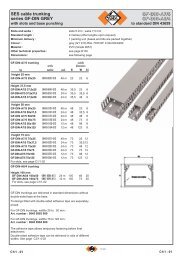
Combination D-Sub Steckverbinder / ConnectorsSkineffektWechselströme erfüllen den Leiterquerschnitt nicht gleichmäßig,sie werden durch Induktionswirkung im Leiter zur Oberfläche hinverdrängt, wobei diese Stromverdrängung mit wachsender Frequenzzunimmt.Die Widerstandsdämpfung einer Übertragungsleitung wird demzufolgemit wachsender Frequenz durch einen zusätzlichen Anteilerhöht, der auf den Skineffekt zurückzuführen ist.Das Eindringmaß (äquivalente Dicke der Schicht, in der dieStromleitung stattfindet), kann bestimmt werden nach1δ =√fπσµ0 µ rf = Frequenzσ = Leitfähigkeit des eingesetzten Leitermaterialsσ Ag= 62 x 10 6 S/mσ Cu= 58 x 10 6 S/mµ 0= 1,256 10 6 Vs / Amµ r... relative Permeabilitätskonstante des benutzten MaterialsSkin effectAlternating currents do not uniformly occupy the entire crosssection of the conductor, rather inductance effect in the conductordeflects the current towards the surface of the conductor, wherebythis deflection increases with the frequency.The resistive attenuation of a transmission line increases wirh thefrequency as a result of this skin effect.The skin depth (equivalent thickness of the layer in wich currentflows) can be determined usingδ =√fπσµ0 µ rf = frequencyσ = conductivity of the conductor meterialσ Ag= 62 x 10 6 S/mσ Cu= 58 x 10 6 S/mµ 0= 1,256 10 6 Vs / Amµ r... relative permeability constant for the employed material1VSWR-WertAls Welligkeit oder Stehwellen-Verhältnis s (mit 1 s 1 ∞) ist dasVerhältnis der Beträge der größten und der kleinsten Spannungauf einer verlustlosen Leitung zu verstehen. Der wechselseitigeWert der Welligkeit wird als Anpassungsfaktor m (mit 0 m 1) bezeichnet.Mit dem ⇒ Reflexionsfaktor auf einer Leitung r ist s über folgendeBeziehung verknüpft(1 + IrI)s =(1 _ IrI)VSWR-ValueThe ratio between the value of the largest and the smallestvoltages on a loss-free line is known as the ripple or voltagestanding wave ratio s (where 1 m 1 ∞). The reciprocal value ofthe VSWR is known as the inverse voltage standing wave ratio m(where 0 m 1).(VSWR = Voltage standing ware ratio)The value of is linked with the ⇒ reflection coefficient r on stransmissionline according to the equation(1 + IrI)s =(1 _ IrI)Strombelastbarkeit / Derating diagramBetriebsstrom in Ampere (A) / Working current in amperes (A)Die Messung erfolgte nachDIN 41640 Teil 3 wobei alle Kontaktein Reihe geschaltet wurden.Für die Messung wurden dieProdukte-Nr.3008W8SXX99A10X bestückt mit132C11049Xsowie3008W8PXX99A10X bestückt mit131C11049Xeingesetzt.GrenztemperaturLimit temperature2|6Measurement is according toDIN 41640 part 3 whereas allcontacts are connected in series.For test procedure - product no.3008W8SXX99A10Xhas been equipped with132C11049Xand3008W8PXX99A10X with131C11049X®Umgebungstemperatur / Ambient temperature (°C)