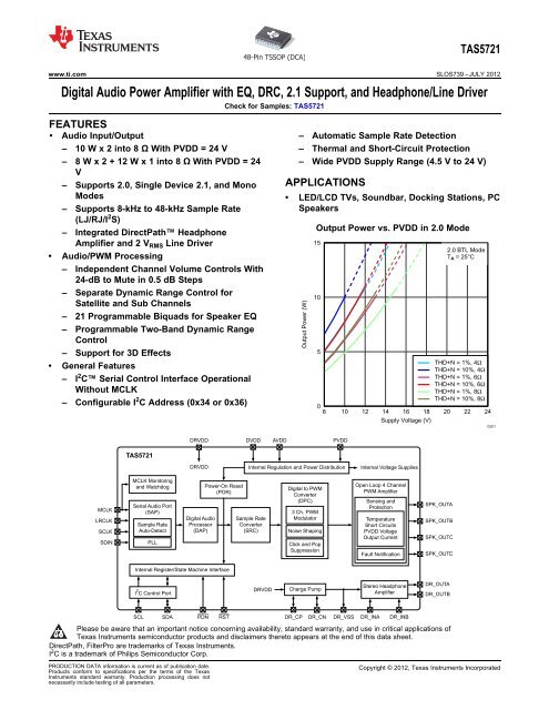
Digital Audio Power Amplifier w/ EQ, DRC, 2.1 Support, and ...
Digital Audio Power Amplifier w/ EQ, DRC, 2.1 Support, and ...
Digital Audio Power Amplifier w/ EQ, DRC, 2.1 Support, and ...

You also want an ePaper? Increase the reach of your titles
YUMPU automatically turns print PDFs into web optimized ePapers that Google loves.
MCLK<br />
LRCLK<br />
SCLK<br />
SDIN<br />
TAS5721<br />
MCLK Monitoring<br />
<strong>and</strong> Watchdog<br />
Serial <strong>Audio</strong> Port<br />
(SAP)<br />
Sample Rate<br />
Auto-Detect<br />
PLL<br />
2<br />
I C Control Port<br />
<strong>Digital</strong> <strong>Audio</strong><br />
Processor<br />
(DAP)<br />
Internal Register/State Machine Interface<br />
SCL SDA<br />
DRVDD<br />
DRVDD<br />
<strong>Power</strong>-On Reset<br />
(POR)<br />
PDN RST<br />
48-Pin TSSOP (DCA)<br />
DVDD<br />
AVDD<br />
Charge Pump<br />
PVDD<br />
Internal Regulation <strong>and</strong> <strong>Power</strong> Distribution<br />
Sample Rate<br />
Converter<br />
(SRC)<br />
DRVDD<br />
Output <strong>Power</strong> (W)<br />
15<br />
10<br />
<strong>Digital</strong> to PWM<br />
Converter<br />
(DPC)<br />
3 Ch. PWM<br />
Modulator<br />
5<br />
Noise Shaping<br />
Click <strong>and</strong> Pop<br />
Suppression<br />
DR_CP DR_CN<br />
THD+N = 1%, 4Ω<br />
THD+N = 10%, 4Ω<br />
THD+N = 1%, 6Ω<br />
THD+N = 10%, 6Ω<br />
THD+N = 1%, 8Ω<br />
THD+N = 10%, 8Ω<br />
0<br />
8 10 12 14 16 18 20 22 24<br />
Supply Voltage (V)<br />
DR_VSS<br />
Internal Voltage Supplies<br />
Open Loop 4 Channel<br />
PWM <strong>Amplifier</strong><br />
Sensing <strong>and</strong><br />
Protection<br />
Temperature<br />
Short Circuits<br />
PVDD Voltage<br />
Output Current<br />
Fault Notification<br />
Stereo Headphone<br />
<strong>Amplifier</strong><br />
DR_INA DR_INB<br />
SPK_OUTA<br />
SPK_OUTB<br />
SPK_OUTC<br />
SPK_OUTD<br />
DR_OUTA<br />
DR_OUTB<br />
TAS5721<br />
www.ti.com SLOS739 –JULY 2012<br />
<strong>Digital</strong> <strong>Audio</strong> <strong>Power</strong> <strong>Amplifier</strong> with <strong>EQ</strong>, <strong>DRC</strong>, <strong>2.1</strong> <strong>Support</strong>, <strong>and</strong> Headphone/Line Driver<br />
Check for Samples: TAS5721<br />
1FEATURES<br />
23• <strong>Audio</strong> Input/Output – Automatic Sample Rate Detection<br />
– 10 W x 2 into 8 Ω With PVDD = 24 V – Thermal <strong>and</strong> Short-Circuit Protection<br />
– 8 W x 2 + 12 W x 1 into 8 Ω With PVDD = 24<br />
V<br />
– Wide PVDD Supply Range (4.5 V to 24 V)<br />
– <strong>Support</strong>s 2.0, Single Device <strong>2.1</strong>, <strong>and</strong> Mono APPLICATIONS<br />
Modes • LED/LCD TVs, Soundbar, Docking Stations, PC<br />
– <strong>Support</strong>s 8-kHz to 48-kHz Sample Rate<br />
(LJ/RJ/I<br />
Speakers<br />
2S) – Integrated DirectPath Headphone<br />
<strong>Amplifier</strong> <strong>and</strong> 2 V RMS Line Driver<br />
• <strong>Audio</strong>/PWM Processing<br />
– Independent Channel Volume Controls With<br />
24-dB to Mute in 0.5 dB Steps<br />
– Separate Dynamic Range Control for<br />
Satellite <strong>and</strong> Sub Channels<br />
– 21 Programmable Biquads for Speaker <strong>EQ</strong><br />
– Programmable Two-B<strong>and</strong> Dynamic Range<br />
Control<br />
– <strong>Support</strong> for 3D Effects<br />
• General Features<br />
– I 2 C Serial Control Interface Operational<br />
Without MCLK<br />
– Configurable I 2 C Address (0x34 or 0x36)<br />
1<br />
Output <strong>Power</strong> vs. PVDD in 2.0 Mode<br />
Please be aware that an important notice concerning availability, st<strong>and</strong>ard warranty, <strong>and</strong> use in critical applications of<br />
Texas Instruments semiconductor products <strong>and</strong> disclaimers thereto appears at the end of this data sheet.<br />
2DirectPath, FilterPro are trademarks of Texas Instruments.<br />
3I 2 C is a trademark of Philips Semiconductor Corp.<br />
2.0 BTL Mode<br />
T A = 25°C<br />
PRODUCTION DATA information is current as of publication date. Copyright © 2012, Texas Instruments Incorporated<br />
Products conform to specifications per the terms of the Texas<br />
Instruments st<strong>and</strong>ard warranty. Production processing does not<br />
necessarily include testing of all parameters.<br />
G001
TAS5721<br />
SLOS739 –JULY 2012 www.ti.com<br />
These devices have limited built-in ESD protection. The leads should be shorted together or the device placed in conductive foam<br />
during storage or h<strong>and</strong>ling to prevent electrostatic damage to the MOS gates.<br />
DESCRIPTION<br />
The TAS5721 is an efficient, digital-input audio amplifier for driving 2.0 speaker systems configured as a bridge<br />
tied load (BTL), <strong>2.1</strong> systems with two satellite speakers <strong>and</strong> one subwoofer, or in PBTL systems driving a single<br />
speaker configured as a parallel bridge tied load (PBTL). One serial data input allows processing of up to two<br />
discrete audio channels <strong>and</strong> seamless integration to most digital audio processors <strong>and</strong> MPEG decoders. The<br />
device accepts a wide range of input data formats <strong>and</strong> sample rates. A fully programmable data path routes<br />
these channels to the internal speaker drivers.<br />
The TAS5721 is a slave-only device, receiving all clocks from external sources. The TAS5721 operates with a<br />
PWM carrier frequency between a 384-kHz switching rate <strong>and</strong> a 288-KHz switching rate, depending on the input<br />
sample rate. Oversampling, combined with a fourth-order noise shaper, provides a flat noise floor <strong>and</strong> excellent<br />
dynamic range from 20 Hz to 20 kHz.<br />
An integrated ground centered DirectPath combination headphone amplifier <strong>and</strong> 2V RMS line driver is integrated<br />
in the TAS5721.<br />
MCLK<br />
LRCLK<br />
SCLK<br />
SDIN<br />
TAS5721<br />
MCLK Monitoring<br />
<strong>and</strong> Watchdog<br />
Serial <strong>Audio</strong> Port<br />
(SAP)<br />
Sample Rate<br />
Auto-Detect<br />
PLL<br />
2<br />
I C Control Port<br />
<strong>Digital</strong> <strong>Audio</strong><br />
Processor<br />
(DAP)<br />
Internal Register/State Machine Interface<br />
SCL SDA<br />
DRVDD<br />
DRVDD<br />
<strong>Power</strong>-On Reset<br />
(POR)<br />
PDN RST<br />
DVDD<br />
AVDD<br />
Charge Pump<br />
PVDD<br />
Internal Regulation <strong>and</strong> <strong>Power</strong> Distribution<br />
Sample Rate<br />
Converter<br />
(SRC)<br />
DRVDD<br />
<strong>Digital</strong> to PWM<br />
Converter<br />
(DPC)<br />
3 Ch. PWM<br />
Modulator<br />
Noise Shaping<br />
Click <strong>and</strong> Pop<br />
Suppression<br />
DR_CP DR_CN<br />
DR_VSS<br />
Figure 1. DAP Process Structure<br />
Internal Voltage Supplies<br />
Open Loop 4 Channel<br />
PWM <strong>Amplifier</strong><br />
Sensing <strong>and</strong><br />
Protection<br />
Temperature<br />
Short Circuits<br />
PVDD Voltage<br />
Output Current<br />
Fault Notification<br />
Stereo Headphone<br />
<strong>Amplifier</strong><br />
DR_INA DR_INB<br />
SPK_OUTA<br />
SPK_OUTB<br />
SPK_OUTC<br />
SPK_OUTD<br />
DR_OUTA<br />
DR_OUTB<br />
2 Submit Documentation Feedback Copyright © 2012, Texas Instruments Incorporated<br />
Product Folder Links: TAS5721
PGND<br />
SPK_OUTA<br />
BSTRPA<br />
PVDD<br />
TEST1<br />
TEST2<br />
DR_INA<br />
DR_OUTA<br />
DR_OUTB<br />
DR_INB<br />
DR_VSS<br />
DR_CN<br />
DR_CP<br />
DRVDD<br />
PLL_GND<br />
PLL_FLTM<br />
PLL_FLTP<br />
AVDD_REG1<br />
AVDD<br />
ADR/FAULT<br />
MCLK<br />
OSC_RES<br />
OSC_GND<br />
DVDD_REG<br />
1<br />
2<br />
3<br />
4<br />
5<br />
6<br />
7<br />
8<br />
9<br />
10<br />
11<br />
12<br />
13<br />
14<br />
15<br />
16<br />
17<br />
18<br />
19<br />
20<br />
21<br />
22<br />
23<br />
24<br />
TAS5721<br />
DCA Package<br />
(Top View)<br />
<strong>Power</strong>PAD<br />
48<br />
47<br />
46<br />
45<br />
44<br />
43<br />
42<br />
41<br />
40<br />
39<br />
38<br />
37<br />
36<br />
35<br />
34<br />
33<br />
32<br />
31<br />
30<br />
29<br />
28<br />
27<br />
26<br />
25<br />
SPK_OUTB<br />
BSTRPB<br />
BSTRPC<br />
SPK_OUTC<br />
PGND<br />
SPK_OUTD<br />
BSTRPD<br />
PVDD<br />
GVDD_REG<br />
DR_SD<br />
SSTIMER<br />
AVDD_REG2<br />
AGND<br />
DGND<br />
DVDD<br />
TEST3<br />
RST<br />
NC<br />
SCL<br />
SDA<br />
SDIN<br />
SCLK<br />
LRCLK<br />
PDN<br />
TAS5721<br />
www.ti.com SLOS739 –JULY 2012<br />
PIN ASSIGNMENT AND DESCRIPTIONS<br />
Pin Out<br />
PIN TYPE (1) TERMINATION DESCRIPTION<br />
NAME NO.<br />
ADR/FAULT 20 DI/DO - Dual function terminal which sets the LSB of the I 2 C address to 0 if pulled<br />
to GND, 1 if pulled to DVDD. If configured to be a fault output by the<br />
methods described in I²C Address Selection <strong>and</strong> Fault Output, this terminal<br />
is pulled low when an internal fault occurs. A pull-up or pull-down resistor is<br />
required, as is shown in the Typical Application Circuit Diagrams.<br />
AGND 36 P - Ground reference for analog circuitry (2)<br />
AVDD 19 P - <strong>Power</strong> supply for internal analog circuitry<br />
AVDD_REG1 18 P - Voltage regulator derived from AVDD supply (3)<br />
AVDD_REG2 37 P - Voltage regulator derived from AVDD supply (3)<br />
BSTRPx 3, 42, 46, P - Connection points for the bootstrap capacitors, which are used to create a<br />
47 power supply for the high-side gate drive of the device<br />
DGND 35 P - Ground reference for digital circuitry (2)<br />
DR_CN 12 P - Negative terminal for capacitor connection used in headphone amplifier<br />
<strong>and</strong> line driver charge pump<br />
DR_CP 13 P - Positive terminal for capacitor connection used in headphone amplifier <strong>and</strong><br />
line driver charge pump<br />
DR_INx 7, 10 AI - Input for channel A or B of headphone amplifier or line driver<br />
(1) TYPE: A = analog; D = 3.3-V digital; P = power/ground/decoupling; I = input; O = output<br />
(2) This terminal should be connected to the system ground<br />
(3) This terminal is provided as a connection point for filtering capacitors for this supply <strong>and</strong> must not be used to power any external<br />
circuitry.<br />
Copyright © 2012, Texas Instruments Incorporated Submit Documentation Feedback 3<br />
Product Folder Links: TAS5721
TAS5721<br />
SLOS739 –JULY 2012 www.ti.com<br />
Pin Out (continued)<br />
DR_OUTx 8, 9 AO - Output for channel A or B of headphone amplifier or line driver<br />
DR_SD 39 DI - Places the headphone amplifier/line driver in shutdown when pulled low.<br />
DR_VSS 11 P - Negative supply generated by charge pump for ground centered<br />
headphone <strong>and</strong> line driver output<br />
DRVDD 14 P - <strong>Power</strong> supply for internal headphone <strong>and</strong> line driver circuitry<br />
DVDD 34 P - <strong>Power</strong> supply for the internal digital circuitry<br />
DVDD_REG 24 P - Voltage regulator derived from DVDD supply (3)<br />
GVDD_REG 40 P - Voltage regulator derived from PVDD supply (3)<br />
LRCLK 26 DI Pulldown Word select clock for the digital signal that is active on the input data line of<br />
the serial port<br />
MCLK 21 DI Pulldown Master clock used for internal clock tree <strong>and</strong> sub-circuit <strong>and</strong> state machine<br />
clocking<br />
NC 31 - - Not connected inside the device (all no connect terminals should be<br />
connected to ground)<br />
OSC_GND 23 P - Ground reference for oscillator circuitry (this terminal should be connected<br />
to the system ground)<br />
OSC_RES 22 AO - Connection point for oscillator trim resistor<br />
PDN 25 DI Pullup Quick powerdown of the device that is used upon an unexpected loss of<br />
PVDD or DVDD power supply in order to quickly transition the outputs of<br />
the speaker amplifier to a 50/50 duty cycle. This quick powerdown feature<br />
avoids the audible anamolies that would occur as a result of loss of either<br />
of the supplies. If this pin is used to place the device into quick powerdown<br />
mode, the RST pin of the device must be toggled before the device is<br />
brought out of quick powerdown.<br />
PGND 1 P - Ground reference for power device circuitry (4)<br />
PLL_FLTM 16 AI/AO - Negative connection point for the PLL loop filter components<br />
PLL_FLTP 17 AI/AO - Positive connection point for the PLL loop filter components<br />
PLL_GND 15 P - Ground reference for PLL circuitry (this terminal should be connected to the<br />
system ground)<br />
<strong>Power</strong>PAD - P - Thermal <strong>and</strong> ground pad thatprovides both an electrical connection to the<br />
ground plane <strong>and</strong> a thermal path to the PCB for heat dissipation. This pad<br />
must be grounded to the system ground.<br />
PVDD 4, 41 P - <strong>Power</strong> supply for internal power circuitry<br />
RST 32 DI Pullup Places the device in reset when pulled low<br />
SCL 30 DI - I 2 C serial control port clock<br />
SCLK 27 DI Pulldown Bit clock for the digital signal that is active on the input data line of the<br />
serial data port<br />
SDA 29 DI/DO - I 2 C serial control port data<br />
SDIN 28 DI Pulldown Data line to the serial data port<br />
SPK_OUTx 2, 43, 45, AO - Speaker amplifier outputs<br />
48<br />
SSTIMER 38 AI - Connection point for the capacitor that is used by the ramp timing circuit,<br />
as described in Output Mode <strong>and</strong> MUX Selection<br />
TEST1 5 DO - Used by TI for testing during device production (this terminal must be left<br />
floating)<br />
TEST2 6 DO - Used by TI for testing during device production (this terminal must be left<br />
floating)<br />
TEST3 33 DI - Used by TI for testing during device production (this terminal must be<br />
connected to GND)<br />
(4) This terminal should be connected to the system ground<br />
4 Submit Documentation Feedback Copyright © 2012, Texas Instruments Incorporated<br />
Product Folder Links: TAS5721
System Processor<br />
<strong>and</strong><br />
Associated Components<br />
C1<br />
10K<br />
1.5 µfd/10 V<br />
0402 X5R<br />
0402<br />
C4<br />
1.5 µfd/10 V<br />
0402 X5R<br />
R1<br />
R4<br />
10K<br />
0402<br />
DNP<br />
DNP<br />
C2<br />
1000 pfd/50 V<br />
0402 COG<br />
GND<br />
C5<br />
1000 pfd/50 V<br />
0402 COG<br />
GND<br />
15k<br />
GND<br />
R2<br />
10K<br />
0402<br />
R3<br />
0<br />
0402<br />
R5<br />
10K<br />
0402<br />
R6<br />
0<br />
0402<br />
DNP<br />
AVDD<br />
AVDD<br />
C3<br />
220 pfd/50 V<br />
0402 COG<br />
FOR PWM<br />
INPUT ONLY<br />
DNP<br />
C6<br />
220 pfd/50 V<br />
0402 COG<br />
C12<br />
10 µfd/6.3 V<br />
0603 X5R<br />
GND<br />
C14<br />
C18<br />
10 µfd/6.3 V<br />
0603 X5R<br />
GND<br />
C13<br />
1 µfd/10 V<br />
0402 X5R<br />
GND<br />
0.047 µfd/16 V<br />
0402 X7R C15<br />
R7<br />
470<br />
4700 pfd/25 V<br />
0402 X7R<br />
0402<br />
GND<br />
GND<br />
R8<br />
470<br />
0402<br />
C16<br />
0.047 µfd/16 V<br />
0402 X7R<br />
C17<br />
4700 pfd/25 V<br />
0402 X7R<br />
C19<br />
0.1 µfd/16 V<br />
0402 X7R<br />
GND<br />
PVDD<br />
+<br />
C8<br />
220 µfd/35 V<br />
M<br />
GND<br />
C9<br />
0.1 µfd/50 V<br />
0402 X7R<br />
GND<br />
GND<br />
C7<br />
0.033 µfd/50 V<br />
0402 X7R<br />
GND<br />
C10<br />
1 µfd/10 V<br />
0402 X5R<br />
C11<br />
1 µfd/10 V<br />
0402 X5R<br />
R9<br />
18.20K<br />
0402<br />
C20<br />
4.7 µfd/6.3 V<br />
0402 X5R<br />
GND<br />
GND<br />
U1<br />
1<br />
PGND<br />
48<br />
SPK_OUTB<br />
2<br />
SPK_OUTA<br />
47<br />
BSTRPB<br />
3<br />
BSTRPA<br />
4<br />
PVDD<br />
46<br />
BSTRPC<br />
5<br />
TEST1<br />
6<br />
TEST2<br />
45<br />
SPK_OUTC<br />
7<br />
8<br />
9<br />
DR_INA<br />
DR_OUTA<br />
DR_OUTB<br />
44<br />
PGND<br />
43<br />
SPK_OUTD<br />
42<br />
BSTRPD<br />
10<br />
DR_INB<br />
11<br />
DR_VSS<br />
41<br />
PVDD<br />
40<br />
GVDD_REG<br />
12<br />
DR_CN<br />
39<br />
DR_SD<br />
13<br />
DR_CP<br />
14<br />
DRVDD<br />
38<br />
SSTIMER<br />
37<br />
15<br />
AVDD_REG2<br />
PLL_GND<br />
36<br />
AGND<br />
16<br />
PLL_FLTM<br />
35<br />
DGND<br />
17<br />
PLL_FLTP<br />
34<br />
DVDD<br />
18<br />
AVDD_REG1<br />
19<br />
AVDD<br />
33<br />
TEST3<br />
32<br />
RST<br />
31<br />
NC<br />
20<br />
ADR/FAULT<br />
30<br />
SCL<br />
21<br />
MCLK<br />
29<br />
SDA<br />
22<br />
OSC_RES<br />
28<br />
SDIN<br />
27<br />
SCLK<br />
23<br />
OSC_GND<br />
26<br />
LRCLK<br />
24<br />
DVDD_REG PDN<br />
25<br />
TAS5721DCA<br />
HTSSOP48-DCA<br />
U1<br />
HTSSOP48-DCA<br />
<strong>Power</strong>PAD<br />
GND<br />
GND<br />
C21<br />
0.033 µfd/50 V<br />
0402 X7R<br />
C22<br />
0.033 µfd/50 V<br />
0402 X7R<br />
C23<br />
0.033 µfd/50 V<br />
0402 X7R<br />
C24<br />
1 µfd/25 V<br />
0603 X5R<br />
C25<br />
2200 pfd/50 V<br />
0402 X7R GND<br />
C26<br />
0.1 µfd/16 V<br />
0402 X7R<br />
GND<br />
GND<br />
GND<br />
GND<br />
GND<br />
GND<br />
C27<br />
330 pfd/50 V<br />
0402 COG<br />
C28<br />
330 pfd/50 V<br />
0402 COG<br />
C29<br />
330 pfd/50 V<br />
0402 COG<br />
C30<br />
330 pfd/50 V<br />
0402 COG<br />
C32<br />
0.1 µfd/50 V<br />
0402 X7R<br />
+<br />
GND GND<br />
C34<br />
0.1 µfd/16 V<br />
0402 X7R<br />
GND GND<br />
R13<br />
18<br />
0603<br />
R14<br />
18<br />
0603<br />
R15<br />
18<br />
0603<br />
R16<br />
18<br />
0603<br />
PVDD<br />
C31<br />
220 µfd/35 V<br />
M<br />
C33<br />
DVDD<br />
10 µfd/6.3 V<br />
0603 X5R<br />
L1<br />
15 µH/3.5 A<br />
A7503AY<br />
L2<br />
15 µH/3.5 A<br />
A7503AY<br />
L3<br />
15 µH/3.5 A<br />
A7503AY<br />
L4<br />
15 µH/3.5 A<br />
A7503AY<br />
C35<br />
0.33 µfd/50 V<br />
0805 X7R<br />
C36<br />
0.33 µfd/50 V<br />
0805 X7R<br />
STUFF<br />
OPTION<br />
C37<br />
0.33 µfd/50 V<br />
0805 X7R<br />
GND<br />
C38<br />
0.33 µfd/50 V<br />
0805 X7R<br />
GND<br />
C39<br />
0.33 µfd/50 V<br />
0805 X7R<br />
GND<br />
C40<br />
0.33 µfd/50 V<br />
0805 X7R<br />
GND<br />
STUFF OPTION NOTE<br />
GROUND REFERENCED CAPS<br />
R<strong>EQ</strong>UIRED IF BD MODULATION<br />
IS USED<br />
TAS5721<br />
www.ti.com SLOS739 –JULY 2012<br />
TYPICAL APPLICATION CIRCUITS<br />
Figure 2. Typical Application Circuit for Mono (PBTL) Configuration<br />
HEADPHONES<br />
OUTPUTS<br />
Copyright © 2012, Texas Instruments Incorporated Submit Documentation Feedback 5<br />
Product Folder Links: TAS5721
TAS5721<br />
SLOS739 –JULY 2012 www.ti.com<br />
System Processor<br />
<strong>and</strong><br />
Associated Components<br />
C1<br />
1.5 µfd/10 V<br />
0402 X5R<br />
C4<br />
1.5 µfd/10 V<br />
0402 X5R<br />
R1<br />
10K<br />
0402<br />
R4<br />
10K<br />
0402<br />
DNP<br />
DNP<br />
C2<br />
1000 pfd/50 V<br />
0402 COG<br />
GND<br />
C5<br />
1000 pfd/50 V<br />
0402 COG<br />
GND<br />
15k<br />
GND<br />
R2<br />
10K<br />
0402<br />
R3<br />
0<br />
0402<br />
R5<br />
10K<br />
0402<br />
R6<br />
0<br />
0402<br />
DNP<br />
AVDD<br />
AVDD<br />
C3<br />
220 pfd/50 V<br />
0402 COG<br />
FOR PWM<br />
INPUT ONLY<br />
DNP<br />
C6<br />
220 pfd/50 V<br />
0402 COG<br />
C12<br />
10 µfd/6.3 V<br />
0603 X5R<br />
GND<br />
C14<br />
0.047 µfd/16 V<br />
0402 X7R<br />
R7<br />
470<br />
0402<br />
GND<br />
R8<br />
470<br />
0402<br />
C16<br />
0.047 µfd/16 V<br />
0402 X7R<br />
C18<br />
10 µfd/6.3 V<br />
0603 X5R<br />
GND<br />
C13<br />
1 µfd/10 V<br />
0402 X5R<br />
GND<br />
C15<br />
4700 pfd/25 V<br />
0402 X7R<br />
GND<br />
C17<br />
4700 pfd/25 V<br />
0402 X7R<br />
C19<br />
0.1 µfd/16 V<br />
0402 X7R<br />
GND<br />
PVDD<br />
+<br />
C8<br />
220 µfd/35 V<br />
M<br />
GND<br />
C9<br />
0.1 µfd/50 V<br />
0402 X7R<br />
GND<br />
GND<br />
DR_INA<br />
DR_OUTA<br />
DR_OUTB<br />
DR_INB<br />
C10<br />
GND<br />
C7<br />
0.033 µfd/50 V<br />
0402 X7R<br />
GND<br />
1 µfd/10 V<br />
0402 X5R<br />
C11<br />
1 µfd/10 V<br />
0402 X5R<br />
C20<br />
R9<br />
18.20K<br />
0402<br />
4.7 µfd/6.3 V<br />
0402 X5R<br />
U1<br />
1<br />
PGND<br />
48<br />
SPK_OUTB<br />
2<br />
SPK_OUTA<br />
47<br />
BSTRPB<br />
3<br />
BSTRPA<br />
4<br />
PVDD<br />
46<br />
BSTRPC<br />
5<br />
TEST1<br />
6<br />
TEST2<br />
45<br />
SPK_OUTC<br />
7<br />
8<br />
9<br />
44<br />
PGND<br />
DR_INA<br />
43<br />
SPK_OUTD<br />
DR_OUTA<br />
42<br />
BSTRPD<br />
DR_OUTB<br />
10<br />
DR_INB<br />
11<br />
DR_VSS<br />
41<br />
PVDD<br />
40<br />
GVDD_REG<br />
U1<br />
HTSSOP48-DCA<br />
<strong>Power</strong>PAD<br />
GND<br />
C21<br />
0.033 µfd/50 V<br />
0402 X7R<br />
C22<br />
0.033 µfd/50 V<br />
0402 X7R<br />
C23<br />
0.033 µfd/50 V<br />
0402 X7R<br />
C24<br />
12<br />
DR_CN DR_SD<br />
39<br />
1 µfd/25 V<br />
0603 X5R<br />
C25<br />
GND<br />
13<br />
DR_CP<br />
14<br />
DRVDD<br />
38<br />
SSTIMER<br />
2200 pfd/50 V<br />
0402 X7R GND<br />
C26<br />
37<br />
15<br />
AVDD_REG2<br />
PLL_GND<br />
36<br />
AGND<br />
16<br />
35<br />
PLL_FLTM DGND<br />
0.1 µfd/16 V<br />
0402 X7R GND<br />
17<br />
PLL_FLTP<br />
34<br />
DVDD<br />
18<br />
AVDD_REG1<br />
19<br />
AVDD<br />
33<br />
TEST3<br />
32<br />
RST<br />
31<br />
NC<br />
20<br />
ADR/FAULT<br />
30<br />
SCL<br />
21<br />
MCLK<br />
29<br />
SDA<br />
22<br />
OSC_RES<br />
28<br />
SDIN<br />
27<br />
SCLK<br />
23<br />
OSC_GND<br />
26<br />
LRCLK<br />
24<br />
DVDD_REG PDN<br />
25<br />
GND<br />
TAS5721DCA<br />
HTSSOP48-DCA<br />
GND<br />
GND<br />
GND<br />
GND<br />
GND<br />
C32<br />
C27<br />
330 pfd/50 V<br />
0402 COG<br />
C28<br />
330 pfd/50 V<br />
0402 COG<br />
C29<br />
330 pfd/50 V<br />
0402 COG<br />
C30<br />
330 pfd/50 V<br />
0402 COG<br />
0.1 µfd/50 V<br />
0402 X7R<br />
GND GND<br />
C34<br />
0.1 µfd/16 V<br />
0402 X7R<br />
GND GND<br />
R13<br />
18<br />
0603<br />
R14<br />
18<br />
0603<br />
R15<br />
18<br />
0603<br />
R16<br />
18<br />
0603<br />
PVDD<br />
+<br />
C31<br />
220 µfd/35 V<br />
M<br />
C33<br />
DVDD<br />
10 µfd/6.3 V<br />
0603 X5R<br />
Figure 3. Typical Application Diagram for 2.0 Configuration<br />
L1<br />
15 µH/3.5 A<br />
A7503AY<br />
L2<br />
15 µH/3.5 A<br />
A7503AY<br />
L3<br />
15 µH/3.5 A<br />
A7503AY<br />
L4<br />
15 µH/3.5 A<br />
A7503AY<br />
C35<br />
0.33 µfd/50 V<br />
0805 X7R<br />
C36<br />
0.33 µfd/50 V<br />
0805 X7R<br />
STUFF<br />
OPTION<br />
C37<br />
0.33 µfd/50 V<br />
0805 X7R<br />
GND<br />
C38<br />
0.33 µfd/50 V<br />
0805 X7R<br />
GND<br />
C39<br />
0.33 µfd/50 V<br />
0805 X7R<br />
GND<br />
C40<br />
0.33 µfd/50 V<br />
0805 X7R<br />
GND<br />
STUFF OPTION NOTE<br />
GROUND REFERENCED CAPS<br />
R<strong>EQ</strong>UIRED IF BD MODULATION<br />
IS USED<br />
HEADPHONES<br />
OUTPUTS<br />
6 Submit Documentation Feedback Copyright © 2012, Texas Instruments Incorporated<br />
Product Folder Links: TAS5721
System Processor<br />
<strong>and</strong><br />
Associated Components<br />
C1<br />
10K<br />
1.5 µfd/10 V<br />
0402<br />
0402 X5R<br />
C4<br />
1.5 µfd/10 V<br />
0402 X5R<br />
R1<br />
R4<br />
10K<br />
0402<br />
DNP<br />
DNP<br />
C2<br />
1000 pfd/50 V<br />
0402 COG<br />
GND<br />
C5<br />
1000 pfd/50 V<br />
0402 COG<br />
GND<br />
15k<br />
GND<br />
R2<br />
10K<br />
0402<br />
R3<br />
0<br />
0402<br />
R5<br />
10K<br />
0402<br />
R6<br />
0<br />
0402<br />
DNP<br />
AVDD<br />
AVDD<br />
C3<br />
220 pfd/50 V<br />
0402 COG<br />
FOR PWM<br />
INPUT ONLY<br />
DNP<br />
C6<br />
220 pfd/50 V<br />
0402 COG<br />
C12<br />
10 µfd/6.3 V<br />
0603 X5R<br />
GND<br />
C14<br />
0.047 µfd/16 V<br />
0402 X7R<br />
R7<br />
470<br />
0402<br />
GND<br />
R8<br />
470<br />
0402<br />
C16<br />
0.047 µfd/16 V<br />
0402 X7R<br />
C18<br />
10 µfd/6.3 V<br />
0603 X5R<br />
GND<br />
C13<br />
1 µfd/10 V<br />
0402 X5R<br />
GND<br />
C15<br />
4700 pfd/25 V<br />
0402 X7R<br />
GND<br />
C17<br />
4700 pfd/25 V<br />
0402 X7R<br />
C19<br />
0.1 µfd/16 V<br />
0402 X7R<br />
GND<br />
PVDD<br />
+<br />
C8<br />
220 µfd/35 V<br />
M<br />
GND<br />
C9<br />
0.1 µfd/50 V<br />
0402 X7R<br />
GND<br />
GND<br />
GND<br />
C7<br />
0.033 µfd/50 V<br />
0402 X7R<br />
GND<br />
C20<br />
C10<br />
1 µfd/10 V<br />
0402 X5R<br />
C11<br />
1 µfd/10 V<br />
0402 X5R<br />
R9<br />
18.20K<br />
0402<br />
4.7 µfd/6.3 V<br />
0402 X5R<br />
U1<br />
1<br />
PGND<br />
48<br />
SPK_OUTB<br />
2<br />
SPK_OUTA<br />
47<br />
BSTRPB<br />
3<br />
BSTRPA<br />
4<br />
PVDD<br />
46<br />
BSTRPC<br />
5<br />
TEST1<br />
6<br />
TEST2<br />
45<br />
SPK_OUTC<br />
7<br />
8<br />
9<br />
44<br />
PGND<br />
DR_INA<br />
43<br />
SPK_OUTD<br />
DR_OUTA<br />
42<br />
BSTRPD<br />
DR_OUTB<br />
10<br />
DR_INB<br />
11<br />
DR_VSS<br />
41<br />
PVDD<br />
40<br />
GVDD_REG<br />
U1<br />
HTSSOP48-DCA<br />
<strong>Power</strong>PAD<br />
GND<br />
C21<br />
0.033 µfd/50 V<br />
0402 X7R<br />
C22<br />
0.033 µfd/50 V<br />
0402 X7R<br />
C23<br />
0.033 µfd/50 V<br />
0402 X7R<br />
C24<br />
12<br />
DR_CN<br />
39<br />
DR_SD<br />
1 µfd/25 V<br />
0603 X5R<br />
C25<br />
GND<br />
13<br />
DR_CP<br />
14<br />
DRVDD<br />
38<br />
SSTIMER<br />
2200 pfd/50 V<br />
0402 X7R GND<br />
C26<br />
37<br />
15<br />
AVDD_REG2<br />
PLL_GND<br />
36<br />
AGND<br />
16<br />
35<br />
PLL_FLTM DGND<br />
0.1 µfd/16 V<br />
0402 X7R GND<br />
17<br />
PLL_FLTP<br />
34<br />
DVDD<br />
18<br />
AVDD_REG1<br />
19<br />
AVDD<br />
33<br />
TEST3<br />
32<br />
RST<br />
31<br />
NC<br />
20<br />
ADR/FAULT<br />
30<br />
SCL<br />
21<br />
MCLK<br />
29<br />
SDA<br />
22<br />
OSC_RES<br />
28<br />
SDIN<br />
27<br />
SCLK<br />
23<br />
OSC_GND<br />
26<br />
LRCLK<br />
24<br />
DVDD_REG PDN<br />
25<br />
GND<br />
TAS5721DCA<br />
HTSSOP48-DCA<br />
GND<br />
GND<br />
GND<br />
GND<br />
GND<br />
C32<br />
C27<br />
330 pfd/50 V<br />
0402 COG<br />
C28<br />
330 pfd/50 V<br />
0402 COG<br />
C29<br />
330 pfd/50 V<br />
0402 COG<br />
C30<br />
330 pfd/50 V<br />
0402 COG<br />
0.1 µfd/50 V<br />
0402 X7R<br />
GND GND<br />
C34<br />
0.1 µfd/16 V<br />
0402 X7R<br />
GND GND<br />
R13<br />
18<br />
0603<br />
R14<br />
18<br />
0603<br />
R15<br />
18<br />
0603<br />
R16<br />
18<br />
0603<br />
PVDD<br />
+<br />
C31<br />
220 µfd/35 V<br />
M<br />
C33<br />
DVDD<br />
10 µfd/6.3 V<br />
0603 X5R<br />
L1<br />
15 µH/3.5 A<br />
A7503AY<br />
L2<br />
15 µH/3.5 A<br />
A7503AY<br />
L3<br />
15 µH/3.5 A<br />
A7503AY<br />
L4<br />
15 µH/3.5 A<br />
A7503AY<br />
C35<br />
0.33 µfd/50 V<br />
0805 X7R<br />
C36<br />
0.33 µfd/50 V<br />
0805 X7R<br />
STUFF<br />
OPTION<br />
STUFF OPTION<br />
PVDD PVDD<br />
+<br />
C41<br />
R17<br />
15K<br />
0402 1/16W<br />
R19<br />
15K<br />
0402 1/16W<br />
R20<br />
15K<br />
0402 1/16W<br />
C37<br />
0.33 µfd/50 V<br />
0805 X7R<br />
GND<br />
C38<br />
0.33 µfd/50 V<br />
0805 X7R<br />
GND<br />
C39<br />
0.33 µfd/50 V<br />
0805 X7R<br />
GND<br />
C40<br />
0.33 µfd/50 V<br />
0805 X7R<br />
GND<br />
STUFF OPTION NOTE<br />
GROUND REFERENCED CAPS<br />
R<strong>EQ</strong>UIRED IF BD MODULATION<br />
IS USED<br />
+<br />
220 µfd/35 V<br />
M<br />
C42<br />
+<br />
R18<br />
15K<br />
0402 1/16W<br />
220 µfd/35 V<br />
M<br />
GND GND<br />
PVDD PVDD<br />
+<br />
C43<br />
220 µfd/35 V<br />
M<br />
C44<br />
220 µfd/35 V<br />
M<br />
GND GND<br />
SPLIT CAP<br />
TAS5721<br />
www.ti.com SLOS739 –JULY 2012<br />
Figure 4. Typical Application Diagram for <strong>2.1</strong> Configuration<br />
HEADPHONES<br />
OUTPUTS<br />
Copyright © 2012, Texas Instruments Incorporated Submit Documentation Feedback 7<br />
Product Folder Links: TAS5721
TAS5721<br />
SLOS739 –JULY 2012 www.ti.com<br />
ABSOLUTE MAXIMUM RATINGS<br />
Over operating free-air temperature range (unless otherwise noted). (1)<br />
Supply voltage<br />
VALUE UNIT<br />
DVDD, AVDD, DRVDD –0.3 to 3.6 V<br />
PVDD –0.3 to 30 V<br />
DR_INx –0.3 to DRVDD + 6 V V<br />
3.3-V digital input –0.5 to DVDD + 0.5<br />
Input voltage 5-V tolerant (2) digital input (except MCLK) –0.5 to DVDD + 2.5 (3)<br />
5-V tolerant MCLK input –0.5 to AVDD + 2.5 (3)<br />
SPK_OUTx to GND 32 (4)<br />
BSTRPx to GND 39 (4)<br />
Operating free-air temperature 0 to 85 °C<br />
Storage temperature range, T stg –40 to 125 °C<br />
(1) Stresses beyond those listed under Absolute Maximum Ratings may cause permanent damage to the device. These are stress ratings<br />
only <strong>and</strong> functional operation of the device at these or any other conditions beyond those indicated under Recommended Operating<br />
Conditions is not implied. Exposure to absolute-maximum conditions for extended periods may affect device reliability.<br />
(2) 5-V tolerant inputs are PDN, RST, SCLK, LRCLK, MCLK, SDIN, SDA, <strong>and</strong> SCL.<br />
(3) Maximum pin voltage should not exceed 6 V.<br />
(4) DC voltage + peak AC waveform measured at the pin should be below the allowed limit for all conditions.<br />
RECOMMENDED OPERATING CONDITIONS<br />
MIN NOM MAX UNIT<br />
xVDD <strong>Digital</strong>, analog, headphone supply 3 3.3 3.6 V<br />
voltage<br />
PVDD Half-bridge supply voltage 8 26.4 (1) V<br />
V IH High-level input voltage 5-V tolerant 2 V<br />
V IL Low-level input voltage 5-V tolerant 0.8 V<br />
T A Operating ambient temperature range 0 85 °C<br />
T J (2) Operating junction temperature range 0 125 °C<br />
RSPK Minimum <strong>Support</strong>ed Speaker<br />
(SE, BTL, <strong>and</strong> Output filter: L = 15 μH, C = 330 nF 4 8 Ω<br />
Impedance<br />
PBTL)<br />
Minimum output inductance<br />
Lo(BTL) Output-filter inductance 10 μH<br />
under short-circuit condition<br />
R HP Headphone mode load impedance 16 32 Ω<br />
R LD Line-diver mode load impedance 0.6 10 kΩ<br />
(1) For operation at PVDD levels greater than 18 V, the modulation limit must be set to 93.8% via the control port register 0x10.<br />
(2) Continuous operation above the recommended junction temperature may result in reduced reliability <strong>and</strong>/or lifetime of the device.<br />
ELECTRICAL CHARACTERISTICS<br />
I/O Pin Characteristics<br />
PVDD = 18 V, AVDD = DRVDD = DVDD = 3.3 V, external components per Typical Application Circuit diagrams, <strong>and</strong> in<br />
accordance with recommended operating conditions (unless otherwise specified).<br />
PARAMETER TEST CONDITIONS MIN TYP MAX UNIT<br />
IOH = –4 mA<br />
VOH High-level output voltage 2.4<br />
DVDD = AVDD = 3 V<br />
ADR/FAULT <strong>and</strong> SDA V<br />
IOL = 4 mA<br />
VOL Low-level output voltage 0.5<br />
DVDD = AVDD = 3 V<br />
VI < VIL ; DVDD = AVDD<br />
IIL Low-level input current 75<br />
= 3.6 V<br />
<strong>Digital</strong> Inputs μA<br />
VI > VIH ; DVDD =<br />
IIH High-level input current 75<br />
AVDD = 3.6 V<br />
8 Submit Documentation Feedback Copyright © 2012, Texas Instruments Incorporated<br />
Product Folder Links: TAS5721<br />
V<br />
V<br />
V
RST<br />
2<br />
I C Active<br />
t w(RST)<br />
t d(I2C_ready)<br />
System Initialization.<br />
2<br />
Enable via I C.<br />
2<br />
I C Active<br />
TAS5721<br />
www.ti.com SLOS739 –JULY 2012<br />
I/O Pin Characteristics (continued)<br />
PVDD = 18 V, AVDD = DRVDD = DVDD = 3.3 V, external components per Typical Application Circuit diagrams, <strong>and</strong> in<br />
accordance with recommended operating conditions (unless otherwise specified).<br />
PARAMETER TEST CONDITIONS MIN TYP MAX UNIT<br />
Normal mode 48 70<br />
3.3 V supply voltage (DVDD,<br />
IDD 3.3 V supply current Reset (RST = low, PDN<br />
mA<br />
AVDD) 21 38<br />
= high, DR_SD = low)<br />
t w(RST) Pulse duration, RST active RST 100 μs<br />
t d(I2C_ready) Time before the I 2 C port is able 12 ms<br />
communicate after RST goes<br />
high<br />
NOTE: On power up, it is recommended that the TAS5721 RST be held LOW for at least 100 μs after DVDD has reached 3<br />
V.<br />
NOTE: If RST is asserted LOW while PDN is LOW, then RST must continue to be held LOW for at least 100 μs after PDN is<br />
deasserted (HIGH).<br />
Master Clock Characteristics (1)<br />
Figure 5. Reset Timing<br />
PVDD = 18 V, AVDD = DRVDD = DVDD = 3.3 V, external components per Typical Application Circuit diagrams, <strong>and</strong> in<br />
accordance with recommended operating conditions (unless otherwise specified).<br />
T0421-01<br />
PARAMETER TEST CONDITIONS MIN TYP MAX UNIT<br />
f MCLK MCLK frequency 2.8224 24.576 MHz<br />
MCLK duty cycle 40% 50% 60%<br />
t r(MCLK) / t f(MCLK) Rise/fall time for MCLK 5 ns<br />
(1) For clocks related to the serial audio port, please see Serial <strong>Audio</strong> Port Timing<br />
Copyright © 2012, Texas Instruments Incorporated Submit Documentation Feedback 9<br />
Product Folder Links: TAS5721
TAS5721<br />
SLOS739 –JULY 2012 www.ti.com<br />
I 2 C Serial Control Port Requirements <strong>and</strong> Specifications<br />
PVDD = 18 V, AVDD = DRVDD = DVDD = 3.3 V, external components per Typical Application Circuit diagrams, <strong>and</strong> in<br />
accordance with recommended operating conditions (unless otherwise specified).<br />
SCL<br />
SDA<br />
SCL<br />
SDA<br />
PARAMETER TEST CONDITIONS MIN MAX UNIT<br />
f SCL Frequency, SCL No wait states 400 kHz<br />
t w(H) Pulse duration, SCL high 0.6 μs<br />
t w(L) Pulse duration, SCL low 1.3 μs<br />
t r Rise time, SCL <strong>and</strong> SDA 300 ns<br />
t f Fall time, SCL <strong>and</strong> SDA 300 ns<br />
t su1 Setup time, SDA to SCL 100 ns<br />
t h1 Hold time, SCL to SDA 0 ns<br />
t (buf) Bus free time between stop <strong>and</strong> start conditions 1.3 μs<br />
t su2 Setup time, SCL to start condition 0.6 μs<br />
t h2 Hold time, start condition to SCL 0.6 μs<br />
t su3 Setup time, SCL to stop condition 0.6 μs<br />
C L Load capacitance for each bus line 400 pF<br />
t w(H) t w(L) t r t f<br />
Start<br />
Condition<br />
t su2<br />
t su1<br />
Figure 6. SCL <strong>and</strong> SDA Timing<br />
t h2<br />
t su3<br />
Figure 7. Start <strong>and</strong> Stop Conditions Timing<br />
t h1<br />
Stop<br />
Condition<br />
10 Submit Documentation Feedback Copyright © 2012, Texas Instruments Incorporated<br />
Product Folder Links: TAS5721<br />
t (buf)<br />
T0027-01<br />
T0028-01
SCLK<br />
(Input)<br />
LRCLK<br />
(Input)<br />
SDIN<br />
t (edge)<br />
t h1<br />
t su1<br />
t r<br />
t su2<br />
t h2<br />
t f<br />
T0026-04<br />
TAS5721<br />
www.ti.com SLOS739 –JULY 2012<br />
Serial <strong>Audio</strong> Port Timing<br />
PVDD = 18 V, AVDD = DRVDD = DVDD = 3.3 V, audio input signal =1 kHz sine wave, BTL, AD mode, f S = 48 kHz, R SPK = 8<br />
Ω, AES17 filter, f PWM = 384 kHz, external components per Typical Application Circuit diagrams, <strong>and</strong> in accordance with<br />
recommended operating conditions (unless otherwise specified).<br />
TEST<br />
PARAMETER MIN TYP MAX UNIT<br />
CONDITIONS<br />
f SCLKIN Frequency, SCLK 32 × f S, 48 × f S, 64 × f S C L = 30 pF 1.024 12.288 MHz<br />
t su1 Setup time, LRCLK to SCLK rising edge 10 ns<br />
t h1 Hold time, LRCLK from SCLK rising edge 10 ns<br />
t su2 Setup time, SDIN to SCLK rising edge 10 ns<br />
t h2 Hold time, SDIN from SCLK rising edge 10 ns<br />
t (edge)<br />
LRCLK frequency 8 48 48 kHz<br />
SCLK duty cycle 40% 50% 60%<br />
LRCLK duty cycle 40% 50% 60%<br />
SCLK rising edges between LRCLK rising edges 32 64<br />
LRCLK clock edge with respect to the falling edge of SCLK –1/4 1/4<br />
t r/t f Rise/fall time for SCLK/LRCLK 8 ns<br />
SCLK<br />
edges<br />
SCLK<br />
period<br />
LRCLK allowable drift before LRCLK reset 4 MCLK<br />
Periods<br />
Figure 8. Serial <strong>Audio</strong> Port Timing<br />
Copyright © 2012, Texas Instruments Incorporated Submit Documentation Feedback 11<br />
Product Folder Links: TAS5721
TAS5721<br />
SLOS739 –JULY 2012 www.ti.com<br />
Speaker <strong>Amplifier</strong> Characteristics<br />
T A = 25°C, PVDD = 18 V, AVDD = DRVDD = DVDD = 3.3 V, audio input signal =1 kHz sine wave, BTL, AD mode, f S = 48<br />
kHz, R SPK = 8 Ω, AES17 filter, f PWM = 384 kHz, external components per Typical Application Circuit diagrams, <strong>and</strong> in<br />
accordance with recommended operating conditions (unless otherwise specified).<br />
PARAMETER TEST CONDITIONS MIN TYP MAX UNIT<br />
PVDD = 18 V, R SPK = 8Ω, 1-kHz input signal 10<br />
PVDD = 12 V, RSPK = 8Ω, 10% THD+N, 1-kHz<br />
input signal<br />
<strong>Power</strong> output per channel of PVDD = 12 V, RSPK = 8Ω, 7% THD+N, 1-kHz input<br />
PoSPK speaker amplifier when used in signal<br />
(BTL) BTL mode (1)<br />
PVDD = 8 V, RSPK = 8Ω, 10% THD+N, 1-kHz input<br />
signal<br />
Po SPK<br />
(PBTL)<br />
PVDD = 8 V, RSPK = 8Ω, 7% THD+N, 1-kHz input<br />
signal<br />
PVDD = 12 V, RSPK = 4Ω,<br />
10% THD+N, 1-kHz input signal<br />
10<br />
<strong>Power</strong> output per channel of<br />
speaker amplifier when used in<br />
PBTL mode<br />
PVDD = 12 V, RSPK = 4Ω,<br />
7% THD+N, 1-kHz input signal<br />
10<br />
(1)<br />
PVDD = 18 V, RSPK = 4Ω,<br />
1-kHz input signal<br />
10<br />
PVDD = 12 V, RSPK = 4 Ω,<br />
<strong>Power</strong> output per channel of<br />
Po 10% THD+N, 1-kHz input signal<br />
SPK speaker amplifier when used in<br />
(SE) SE mode PVDD = 24 V, RSPK = 4 Ω,<br />
(1)<br />
10% THD+N, 1-kHz input signal<br />
PVDD = 18 V, PO = 1 W 0.07<br />
THD+N<br />
Total harmonic distortion +<br />
noise<br />
PVDD = 12 V, PO = 1 W 0.11 %<br />
PVDD = 8 V, PO = 1 W 0.2<br />
ICN Idle channel noise A-weighted 61 μV<br />
Crosstalk<br />
P O = 1 W, f = 1 kHz (BD Mode), PVDD = 24 V 58 dB<br />
P O =1 W, f = 1 kHz (AD Mode), PVDD = 24 V 48 dB<br />
A-weighted, f = 1 kHz, maximum power at THD <<br />
SNR Signal-to-noise ratio (2) 106 dB<br />
1%<br />
11.025/22.05/44.1-kHz data rate ±2% 352.8<br />
f PWM Output switching frequency kHz<br />
48/24/12/8/16/32-kHz data rate ±2% 384<br />
Normal mode 32 50<br />
IPVDD Supply current No load (PVDD) Reset (RST = low, PDN =<br />
high)<br />
5 8<br />
mA<br />
Drain-to-source resistance (for<br />
r DS(on) each of the Low-Side <strong>and</strong> High- T J = 25°C, includes metallization resistance 200 mΩ<br />
Side Devices)<br />
Internal pulldown resistor at the Connected when drivers are in the high-impedance<br />
R PD 3 kΩ<br />
output of each half-bridge state to provide bootstrap capacitor charge.<br />
(1) <strong>Power</strong> levels are thermally limited.<br />
(2) SNR is calculated relative to 0-dBFS input level.<br />
12 Submit Documentation Feedback Copyright © 2012, Texas Instruments Incorporated<br />
Product Folder Links: TAS5721<br />
8.8<br />
8.3<br />
4<br />
3.8<br />
4.3<br />
5.5<br />
W
TAS5721<br />
www.ti.com SLOS739 –JULY 2012<br />
Headphone <strong>Amplifier</strong> <strong>and</strong> Line Driver Characteristics<br />
T A = 25°C, PVDD = 18 V, AVDD = DRVDD = DVDD = 3.3 V, audio input signal =1 kHz sine wave, BTL, AD mode, f S = 48<br />
kHz, R SPK = 8 Ω, AES17 filter, f PWM = 384 kHz, external components per Typical Application Circuit diagrams, <strong>and</strong> in<br />
accordance with recommended operating conditions (unless otherwise specified).<br />
PARAMETER TEST CONDITIONS MIN TYP MAX UNIT<br />
Po HP <strong>Power</strong> output per channel of DRVDD = 3.3 V (R HP = 32; THD = 1%) 50 mW<br />
headphone amplifier<br />
AV DR Gain for headphone amplifier <strong>and</strong> line Adjustable through R in <strong>and</strong> R fb - dB<br />
driver<br />
SNR HP Signal-to-noise ratio (headphone mode) R hp = 32 101 dB<br />
SNR LD Signal-to-noise ratio (line driver mode) 2-V RMS output 105 dB<br />
Protection Characteristics<br />
T A = 25°C, PVDD = 18 V, AVDD = DRVDD = DVDD = 3.3 V, audio input signal =1 kHz sine wave, BTL, AD mode, f S = 48<br />
kHz, R SPK = 8 Ω, AES17 filter, f PWM = 384 kHz, external components per Typical Application Circuit diagrams, <strong>and</strong> in<br />
accordance with recommended operating conditions (unless otherwise specified).<br />
PARAMETER TEST CONDITIONS MIN TYP MAX UNIT<br />
V uvp(fall) Undervoltage protection limit PVDD falling 4 V<br />
V uvp(rise) Undervoltage protection limit PVDD rising 4.1 V<br />
OTE Overtemperature error threshold 150 °C<br />
ΔOTE Variation in overtemperature detection circuit ±15 °C<br />
I OCE Overcurrent limit protection threshold 3.0 A<br />
t OCE Overcurrent response time 150 ns<br />
THERMAL CHARACTERISTICS<br />
TAS5721<br />
THERMAL METRIC (1) DCA UNITS<br />
48 PINS<br />
θ JA Junction-to-ambient thermal resistance (2) 27.9<br />
θ JCtop Junction-to-case (top) thermal resistance (3) 20.7<br />
θ JB Junction-to-board thermal resistance (4) 13<br />
ψ JT Junction-to-top characterization parameter (5) 0.3<br />
ψ JB Junction-to-board characterization parameter (6) 6.7<br />
θ JCbot Junction-to-case (bottom) thermal resistance (7) 1.1<br />
(1) For more information about traditional <strong>and</strong> new thermal metrics, see the IC Package Thermal Metrics application report, SPRA953.<br />
(2) The junction-to-ambient thermal resistance under natural convection is obtained in a simulation on a JEDEC-st<strong>and</strong>ard, high-K board, as<br />
specified in JESD51-7, in an environment described in JESD51-2a.<br />
(3) The junction-to-case (top) thermal resistance is obtained by simulating a cold plate test on the package top. No specific JEDECst<strong>and</strong>ard<br />
test exists, but a close description can be found in the ANSI SEMI st<strong>and</strong>ard G30-88.<br />
(4) The junction-to-board thermal resistance is obtained by simulating in an environment with a ring cold plate fixture to control the PCB<br />
temperature, as described in JESD51-8.<br />
(5) The junction-to-top characterization parameter, ψ JT, estimates the junction temperature of a device in a real system <strong>and</strong> is extracted<br />
from the simulation data for obtaining θ JA, using a procedure described in JESD51-2a (sections 6 <strong>and</strong> 7).<br />
(6) The junction-to-board characterization parameter, ψ JB, estimates the junction temperature of a device in a real system <strong>and</strong> is extracted<br />
from the simulation data for obtaining θ JA , using a procedure described in JESD51-2a (sections 6 <strong>and</strong> 7).<br />
(7) The junction-to-case (bottom) thermal resistance is obtained by simulating a cold plate test on the exposed (power) pad. No specific<br />
JEDEC st<strong>and</strong>ard test exists, but a close description can be found in the ANSI SEMI st<strong>and</strong>ard G30-88.<br />
Spacer<br />
Copyright © 2012, Texas Instruments Incorporated Submit Documentation Feedback 13<br />
Product Folder Links: TAS5721<br />
°C/W
TAS5721<br />
SLOS739 –JULY 2012 www.ti.com<br />
Output <strong>Power</strong> (W)<br />
THD+N (%)<br />
8<br />
5<br />
10<br />
1<br />
0.1<br />
0.01<br />
<strong>2.1</strong> SE Mode<br />
T A = 25°C<br />
TYPICAL PERFORMANCE CHARACTERISTICS<br />
SPACER SPACER<br />
SPACER SPACER<br />
OUTPUT POWER OUTPUT POWER<br />
vs vs<br />
PVDD IN <strong>2.1</strong> MODE PVDD IN PBTL MODE<br />
25<br />
PBTL Mode<br />
TA = 25°C<br />
THD+N = 1%, 2x8+8Ω<br />
THD+N = 10%, 2x8+8Ω<br />
THD+N = 1%, 2x8+4Ω<br />
THD+N = 10%, 2x8+4Ω<br />
0<br />
8 10 12 14 16 18 20 22 24<br />
Supply Voltage (V)<br />
SPACER SPACER<br />
SPACER SPACER<br />
TOTAL HARMONIC DISTORTION + NOISE TOTAL HARMONIC DISTORTION + NOISE<br />
vs vs<br />
FR<strong>EQ</strong>UENCY IN 2.0 MODE WITH PVDD = 12 V FR<strong>EQ</strong>UENCY in 2.0 MODE WITH PVDD = 18 V<br />
10<br />
2.0 BTL Mode<br />
2.0 BTL Mode<br />
PVDD = 12V<br />
PVDD = 18V<br />
PO = 1W<br />
PO = 1W<br />
TA = 25°C<br />
TA = 25°C<br />
RL = 4Ω<br />
RL = 6Ω<br />
RL = 8Ω<br />
0.001<br />
20 100 1k 10k 20k<br />
Frequency (Hz)<br />
G002<br />
G004<br />
Output <strong>Power</strong> (W)<br />
THD+N (%)<br />
20<br />
15<br />
10<br />
1<br />
0.1<br />
0.01<br />
5<br />
THD+N = 1%, 4Ω<br />
THD+N = 10%, 4Ω<br />
THD+N = 1%, 6Ω<br />
THD+N = 10%, 6Ω<br />
THD+N = 1%, 8Ω<br />
THD+N = 10%, 8Ω<br />
0<br />
8 10 12 14 16 18 20 22 24<br />
Supply Voltage (V)<br />
Figure 9. Figure 10.<br />
RL = 4Ω<br />
RL = 6Ω<br />
RL = 8Ω<br />
0.001<br />
20 100 1k 10k 20k<br />
Frequency (Hz)<br />
Figure 11. Figure 12.<br />
14 Submit Documentation Feedback Copyright © 2012, Texas Instruments Incorporated<br />
Product Folder Links: TAS5721<br />
G003<br />
G005
THD+N (%)<br />
THD+N (%)<br />
10<br />
1<br />
0.1<br />
0.01<br />
RL = 4Ω<br />
RL = 6Ω<br />
RL = 8Ω<br />
0.001<br />
20 100 1k 10k 20k<br />
Frequency (Hz)<br />
10<br />
1<br />
0.1<br />
0.01<br />
FR<strong>EQ</strong>UENCY IN 2.0 MODE WITH PVDD = 24 V F<strong>EQ</strong>UENCY IN <strong>2.1</strong> MODE WITH PVDD = 12 V<br />
10<br />
2.0 BTL Mode<br />
<strong>2.1</strong> SE Mode<br />
PVDD = 24V<br />
PVDD = 12V<br />
PO = 1W<br />
PO = 1W<br />
TA = 25°C<br />
TA = 25°C<br />
SPACER SPACER<br />
SPACER SPACER<br />
TOTAL HARMONIC DISTORTION + NOISE TOTAL HARMONIC DISTORTION + NOISE<br />
vs vs<br />
FR<strong>EQ</strong>UENCY IN <strong>2.1</strong> MODE WITH PVDD = 18 V FR<strong>EQ</strong>UENCY IN <strong>2.1</strong> MODE WITH PVDD = 24 V<br />
10<br />
<strong>2.1</strong> SE Mode<br />
<strong>2.1</strong> SE Mode<br />
PVDD = 18V<br />
PVDD = 24V<br />
PO = 1W<br />
PO = 1W<br />
TA = 25°C<br />
TA = 25°C<br />
RL = 2x8+8Ω<br />
RL = 2x8+4Ω<br />
RL = 2x4+8Ω<br />
RL = 2x4+4Ω<br />
0.001<br />
20 100 1k 10k 20k<br />
Frequency (Hz)<br />
G006<br />
G009<br />
THD+N (%)<br />
THD+N (%)<br />
1<br />
0.1<br />
0.01<br />
RL = 2x8+8Ω<br />
RL = 2x8+4Ω<br />
RL = 2x4+8Ω<br />
RL = 2x4+4Ω<br />
0.001<br />
20 100 1k 10k 20k<br />
Frequency (Hz)<br />
1<br />
0.1<br />
0.01<br />
TAS5721<br />
www.ti.com SLOS739 –JULY 2012<br />
TYPICAL PERFORMANCE CHARACTERISTICS (continued)<br />
SPACER SPACER<br />
SPACER SPACER<br />
TOTAL HARMONIC DISTORTION + NOISE TOTAL HARMONIC DISTORTION + NOISE<br />
vs vs<br />
Figure 13. Figure 14.<br />
RL = 2x8+8Ω<br />
RL = 2x8+4Ω<br />
RL = 2x4+8Ω<br />
0.001<br />
20 100 1k 10k 20k<br />
Frequency (Hz)<br />
Figure 15. Figure 16.<br />
Copyright © 2012, Texas Instruments Incorporated Submit Documentation Feedback 15<br />
Product Folder Links: TAS5721<br />
G007<br />
G009
TAS5721<br />
SLOS739 –JULY 2012 www.ti.com<br />
THD+N (%)<br />
THD+N (%)<br />
FR<strong>EQ</strong>UENCY IN PBTL MODE WITH PVDD = 12 V FR<strong>EQ</strong>UENCY IN PBTL MODE WITH PVDD = 18 V<br />
10<br />
10<br />
PBTL Mode<br />
PBTL Mode<br />
PVDD = 12V<br />
PVDD = 18V<br />
PO = 1W<br />
PO = 1W<br />
TA = 25°C<br />
TA = 25°C<br />
1<br />
0.1<br />
0.01<br />
RL = 4Ω<br />
RL = 6Ω<br />
RL = 8Ω<br />
0.001<br />
20 100 1k 10k 20k<br />
Frequency (Hz)<br />
SPACER SPACER<br />
SPACER SPACER<br />
TOTAL HARMONIC DISTORTION + NOISE 2.0 IDLE CHANNEL NOISE<br />
vs vs<br />
FR<strong>EQ</strong>UENCY IN PBTL MODE WITH PVDD = 24 V PVDD<br />
10<br />
60<br />
PBTL Mode<br />
2.0 BTL Mode<br />
PVDD = 24V<br />
PO = 1W<br />
TA = 25°C<br />
TA = 25°C<br />
50<br />
1<br />
0.1<br />
0.01<br />
TYPICAL PERFORMANCE CHARACTERISTICS (continued)<br />
SPACER SPACER<br />
SPACER SPACER<br />
TOTAL HARMONIC DISTORTION + NOISE TOTAL HARMONIC DISTORTION + NOISE<br />
vs vs<br />
RL = 4Ω<br />
RL = 6Ω<br />
RL = 8Ω<br />
0.001<br />
20 100 1k 10k 20k<br />
Frequency (Hz)<br />
G010<br />
G012<br />
THD+N (%)<br />
Idle Channel Noise (µV)<br />
1<br />
0.1<br />
0.01<br />
RL = 4Ω<br />
RL = 6Ω<br />
RL = 8Ω<br />
0.001<br />
20 100 1k 10k 20k<br />
Frequency (Hz)<br />
Figure 17. Figure 18.<br />
40<br />
30<br />
20<br />
RL = 4Ω<br />
RL = 6Ω<br />
RL = 8Ω<br />
10<br />
8 10 12 14 16 18 20 22 24<br />
Supply Voltage (V)<br />
Figure 19. Figure 20.<br />
16 Submit Documentation Feedback Copyright © 2012, Texas Instruments Incorporated<br />
Product Folder Links: TAS5721<br />
G011<br />
G013
Idle Channel Noise (µV)<br />
THD+N (%)<br />
45<br />
40<br />
35<br />
30<br />
25<br />
20<br />
15<br />
RL = 2x8+8Ω<br />
RL = 2x4+8Ω<br />
RL = 2x4+4Ω<br />
10<br />
8 10 12 14 16 18 20 22 24<br />
Supply Voltage (V)<br />
SPACER SPACER<br />
SPACER SPACER<br />
TOTAL HARMONIC DISTORTION + NOISE TOTAL HARMONIC DISTORTION + NOISE<br />
vs vs<br />
OUTPUT POWER IN 2.0 MODE WITH PVDD = 12 V OUTPUT POWER IN 2.0 MODE WITH PVDD = 18 V<br />
10<br />
10<br />
2.0 BTL Mode<br />
2.0 BTL Mode<br />
PVDD = 12V<br />
PVDD = 18V<br />
f = 1kHz<br />
f = 1kHz<br />
TA = 25°C<br />
TA = 25°C<br />
1<br />
0.1<br />
<strong>2.1</strong> SE Mode<br />
T A = 25°C<br />
PVDD PVDD<br />
60<br />
PBTL Mode<br />
TA = 25°C<br />
55<br />
RL = 4Ω<br />
RL = 6Ω<br />
RL = 8Ω<br />
0.01<br />
0.01 0.1<br />
Output <strong>Power</strong> (W)<br />
1 10<br />
G014<br />
G016<br />
Idle Channel Noise (µV)<br />
THD+N (%)<br />
50<br />
45<br />
40<br />
35<br />
30<br />
25<br />
20<br />
RL = 4Ω<br />
RL = 8Ω<br />
15<br />
8 10 12 14 16 18 20 22 24<br />
Supply Voltage (V)<br />
1<br />
0.1<br />
TAS5721<br />
www.ti.com SLOS739 –JULY 2012<br />
TYPICAL PERFORMANCE CHARACTERISTICS (continued)<br />
SPACER SPACER<br />
SPACER SPACER<br />
<strong>2.1</strong> IDLE CHANNEL NOISE PBTL IDLE CHANNEL NOISE<br />
vs vs<br />
Figure 21. Figure 22.<br />
RL = 4Ω<br />
RL = 6Ω<br />
RL = 8Ω<br />
0.01<br />
0.01 0.1<br />
Output <strong>Power</strong> (W)<br />
1 10<br />
Figure 23. Figure 24.<br />
Copyright © 2012, Texas Instruments Incorporated Submit Documentation Feedback 17<br />
Product Folder Links: TAS5721<br />
G015<br />
G017
TAS5721<br />
SLOS739 –JULY 2012 www.ti.com<br />
THD+N (%)<br />
THD+N (%)<br />
OUTPUT POWER IN 2.0 MODE WITH PVDD = 24 V OUTPUT POWER IN <strong>2.1</strong> MODE WITH PVDD = 12 V<br />
10<br />
10<br />
2.0 BTL Mode<br />
<strong>2.1</strong> SE Mode<br />
PVDD = 24V<br />
PVDD = 12V<br />
f = 1kHz<br />
f = 1kHz<br />
TA = 25°C<br />
TA = 25°C<br />
1<br />
0.1<br />
RL = 4Ω<br />
RL = 6Ω<br />
RL = 8Ω<br />
0.01<br />
0.01 0.1<br />
Output <strong>Power</strong> (W)<br />
1 10<br />
SPACER SPACER<br />
SPACER SPACER<br />
TOTAL HARMONIC DISTORTION + NOISE TOTAL HARMONIC DISTORTION + NOISE<br />
vs vs<br />
OUTPUT POWER IN <strong>2.1</strong> MODE WITH PVDD = 18 V OUTPUT POWER IN <strong>2.1</strong> MODE WITH PVDD = 24 V<br />
10<br />
10<br />
<strong>2.1</strong> SE Mode<br />
<strong>2.1</strong> SE Mode<br />
PVDD = 18V<br />
PVDD = 24V<br />
f = 1kHz<br />
f = 1kHz<br />
TA = 25°C<br />
TA = 25°C<br />
1<br />
0.1<br />
0.01<br />
TYPICAL PERFORMANCE CHARACTERISTICS (continued)<br />
SPACER SPACER<br />
SPACER SPACER<br />
TOTAL HARMONIC DISTORTION + NOISE TOTAL HARMONIC DISTORTION + NOISE<br />
vs vs<br />
RL = 2x8+8Ω<br />
RL = 2x4+8Ω<br />
RL = 2x4+4Ω<br />
0.001<br />
0.01 0.1<br />
Output <strong>Power</strong> (W)<br />
1 5<br />
G018<br />
G020<br />
THD+N (%)<br />
THD+N (%)<br />
1<br />
0.1<br />
0.01<br />
RL = 2x8+8Ω<br />
RL = 2x4+8Ω<br />
RL = 2x4+4Ω<br />
0.001<br />
0.01 0.1<br />
Output <strong>Power</strong> (W)<br />
1 5<br />
Figure 25. Figure 26.<br />
1<br />
0.1<br />
0.01<br />
RL = 2x8+8Ω<br />
RL = 2x4+8Ω<br />
0.001<br />
0.01 0.1<br />
Output <strong>Power</strong> (W)<br />
1 5<br />
Figure 27. Figure 28.<br />
18 Submit Documentation Feedback Copyright © 2012, Texas Instruments Incorporated<br />
Product Folder Links: TAS5721<br />
G019<br />
G021
THD+N (%)<br />
THD+N (%)<br />
OUTPUT POWER IN PBTL MODE WITH PVDD = 12 V OUTPUT POWER IN PBTL MODE WITH PVDD = 18 V<br />
10<br />
10<br />
PBTL Mode<br />
PBTL Mode<br />
PVDD = 12V<br />
PVDD = 18V<br />
f = 1kHz<br />
f = 1kHz<br />
TA = 25°C<br />
TA = 25°C<br />
1<br />
0.1<br />
0.01<br />
RL = 4Ω<br />
RL = 6Ω<br />
RL = 8Ω<br />
0.001<br />
0.01 0.1 1<br />
Output <strong>Power</strong> (W)<br />
10 20<br />
SPACER SPACER<br />
SPACER SPACER<br />
TOTAL HARMONIC DISTORTION + NOISE EFFICIENCY<br />
vs vs<br />
OUTPUT POWER IN PBTL MODE WITH PVDD = 24 V OUTPUT POWER IN 2.0 MODE<br />
10<br />
100<br />
PBTL Mode<br />
PVDD = 24V<br />
f = 1kHz<br />
90<br />
TA = 25°C<br />
80<br />
1<br />
70<br />
0.1<br />
0.01<br />
RL = 4Ω<br />
RL = 6Ω<br />
RL = 8Ω<br />
0.001<br />
0.01 0.1 1<br />
Output <strong>Power</strong> (W)<br />
10 20<br />
G022<br />
G024<br />
THD+N (%)<br />
Efficiency (%)<br />
1<br />
0.1<br />
0.01<br />
RL = 4Ω<br />
RL = 6Ω<br />
RL = 8Ω<br />
0.001<br />
0.01 0.1 1<br />
Output <strong>Power</strong> (W)<br />
10 20<br />
60<br />
50<br />
40<br />
TAS5721<br />
www.ti.com SLOS739 –JULY 2012<br />
TYPICAL PERFORMANCE CHARACTERISTICS (continued)<br />
SPACER SPACER<br />
SPACER SPACER<br />
TOTAL HARMONIC DISTORTION + NOISE TOTAL HARMONIC DISTORTION + NOISE<br />
vs vs<br />
Figure 29. Figure 30.<br />
30<br />
20<br />
10<br />
PVDD = 12V<br />
PVDD = 18V<br />
PVDD = 24V 2.0 BTL Mode<br />
RL = 8Ω<br />
TA = 25°C<br />
All Channels Driven<br />
0<br />
0 5 10<br />
Total Output <strong>Power</strong> (W)<br />
15 20<br />
G025<br />
All channels driven<br />
Figure 31. Figure 32.<br />
Copyright © 2012, Texas Instruments Incorporated Submit Documentation Feedback 19<br />
Product Folder Links: TAS5721<br />
G023
TAS5721<br />
SLOS739 –JULY 2012 www.ti.com<br />
Efficiency (%)<br />
Efficiency (%)<br />
100<br />
90<br />
80<br />
70<br />
60<br />
50<br />
40<br />
30<br />
20<br />
10<br />
PVDD = 12V<br />
PVDD = 18V<br />
PVDD = 24V <strong>2.1</strong> SE Mode<br />
RL = 2x8+8Ω<br />
TA = 25°C<br />
All Channels Driven<br />
0<br />
0 5 10 15 20 25 30<br />
Total Output <strong>Power</strong> (W)<br />
G026<br />
100<br />
90<br />
80<br />
70<br />
60<br />
50<br />
40<br />
TYPICAL PERFORMANCE CHARACTERISTICS (continued)<br />
SPACER SPACER<br />
SPACER SPACER<br />
EFFICIENCY EFFICIENCY<br />
vs vs<br />
OUTPUT POWER IN <strong>2.1</strong> MODE OUTPUT POWER IN <strong>2.1</strong> MODE<br />
100<br />
SPACER SPACER<br />
SPACER SPACER<br />
EFFICIENCY EFFICIENCY<br />
vs vs<br />
OUTPUT POWER IN PBTL MODE OUTPUT POWER IN PBTL MODE<br />
100<br />
30<br />
20<br />
10<br />
PVDD = 12V<br />
PVDD = 18V<br />
PVDD = 24V PBTL Mode<br />
RL = 8Ω<br />
TA = 25°C<br />
All Channels Driven<br />
0<br />
0 5 10 15 20 25 30<br />
Total Output <strong>Power</strong> (W)<br />
G029<br />
Efficiency (%)<br />
Efficiency (%)<br />
90<br />
80<br />
70<br />
60<br />
50<br />
40<br />
30<br />
20<br />
10<br />
PVDD = 12V<br />
PVDD = 18V<br />
PVDD = 24V <strong>2.1</strong> SE Mode<br />
RL = 2x4+8Ω<br />
TA = 25°C<br />
All Channels Driven<br />
0<br />
0 5 10 15 20 25 30<br />
Total Output <strong>Power</strong> (W)<br />
G027<br />
All channels driven All channels driven<br />
Figure 33. Figure 34.<br />
90<br />
80<br />
70<br />
60<br />
50<br />
40<br />
30<br />
20<br />
10<br />
PVDD = 12V<br />
PVDD = 18V<br />
PVDD = 24V PBTL Mode<br />
RL = 6Ω<br />
TA = 25°C<br />
All Channels Driven<br />
0<br />
0 5 10 15 20 25 30<br />
Total Output <strong>Power</strong> (W)<br />
G030<br />
All channels driven All channels driven<br />
Figure 35. Figure 36.<br />
20 Submit Documentation Feedback Copyright © 2012, Texas Instruments Incorporated<br />
Product Folder Links: TAS5721
Crosstalk (dB)<br />
Crosstalk (dB)<br />
0<br />
−10<br />
−20<br />
−30<br />
−40<br />
−50<br />
−60<br />
−70<br />
−80<br />
−90<br />
−100<br />
20 100 1k<br />
Frequency (Hz)<br />
10k 20k<br />
0<br />
−10<br />
−20<br />
−30<br />
−40<br />
−50<br />
−60<br />
−70<br />
−80<br />
−90<br />
FR<strong>EQ</strong>UENCY IN 2.0 MODE FR<strong>EQ</strong>UENCY IN 2.0 MODE<br />
0<br />
2.0 BTL Mode<br />
Right to Left<br />
2.0 BTL Mode<br />
PO = 1W<br />
PVDD = 12V<br />
Left to Right<br />
−10<br />
PO = 1W<br />
PVDD = 12V<br />
RL = 4Ω<br />
TA = 25°C<br />
−20<br />
RL = 8Ω<br />
TA = 25°C<br />
SPACER SPACER<br />
SPACER SPACER<br />
CROSSTALK CROSSTALK<br />
vs vs<br />
FR<strong>EQ</strong>UENCY IN 2.0 MODE FR<strong>EQ</strong>UENCY IN 2.0 MODE<br />
0<br />
2.0 BTL Mode<br />
Right to Left<br />
2.0 BTL Mode<br />
PO = 1W<br />
PVDD = 24V<br />
Left to Right<br />
−10<br />
PO = 1W<br />
PVDD = 24V<br />
RL = 4Ω<br />
TA = 25°C<br />
−20<br />
RL = 8Ω<br />
TA = 25°C<br />
−100<br />
20 100 1k<br />
Frequency (Hz)<br />
10k 20k<br />
G032<br />
G034<br />
Crosstalk (dB)<br />
Crosstalk (dB)<br />
−30<br />
−40<br />
−50<br />
−60<br />
−70<br />
−80<br />
−90<br />
−100<br />
20 100 1k<br />
Frequency (Hz)<br />
10k 20k<br />
−30<br />
−40<br />
−50<br />
−60<br />
−70<br />
−80<br />
−90<br />
TAS5721<br />
www.ti.com SLOS739 –JULY 2012<br />
TYPICAL PERFORMANCE CHARACTERISTICS (continued)<br />
SPACER SPACER<br />
SPACER SPACER<br />
CROSSTALK CROSSTALK<br />
vs vs<br />
Figure 37. Figure 38.<br />
Right to Left<br />
Left to Right<br />
Right to Left<br />
Left to Right<br />
−100<br />
20 100 1k<br />
Frequency (Hz)<br />
10k 20k<br />
Figure 39. Figure 40.<br />
Copyright © 2012, Texas Instruments Incorporated Submit Documentation Feedback 21<br />
Product Folder Links: TAS5721<br />
G033<br />
G035
TAS5721<br />
SLOS739 –JULY 2012 www.ti.com<br />
Crosstalk (dB)<br />
Crosstalk (dB)<br />
0<br />
−10<br />
−20<br />
−30<br />
−40<br />
−50<br />
−60<br />
−70<br />
−80<br />
−90<br />
−100<br />
20 100 1k<br />
Frequency (Hz)<br />
10k 20k<br />
0<br />
−10<br />
−20<br />
−30<br />
−40<br />
−50<br />
−60<br />
−70<br />
−80<br />
−90<br />
TYPICAL PERFORMANCE CHARACTERISTICS (continued)<br />
SPACER SPACER<br />
SPACER SPACER<br />
CROSSTALK CROSSTALK<br />
vs vs<br />
FR<strong>EQ</strong>UENCY IN <strong>2.1</strong> MODE FR<strong>EQ</strong>UENCY IN <strong>2.1</strong> MODE<br />
0<br />
<strong>2.1</strong> SE Mode<br />
Right to Left<br />
<strong>2.1</strong> SE Mode<br />
PO = 1W<br />
PVDD = 12V<br />
Left to Right<br />
−10<br />
PO = 1W<br />
PVDD = 12V<br />
RL = 2x8+8Ω<br />
TA = 25°C<br />
−20<br />
RL =2x4+8Ω<br />
TA = 25°C<br />
SPACER SPACER<br />
SPACER SPACER<br />
CROSSTALK CROSSTALK<br />
vs vs<br />
FR<strong>EQ</strong>UENCY IN <strong>2.1</strong> MODE FR<strong>EQ</strong>UENCY IN <strong>2.1</strong> MODE<br />
0<br />
<strong>2.1</strong> SE Mode<br />
Right to Left<br />
<strong>2.1</strong> SE Mode<br />
PO = 1W<br />
PVDD = 24V<br />
Left to Right<br />
−10<br />
PO = 1W<br />
PVDD = 24V<br />
RL = 2x8+8Ω<br />
TA = 25°C<br />
−20<br />
RL =2x4+8Ω<br />
TA = 25°C<br />
−100<br />
20 100 1k<br />
Frequency (Hz)<br />
10k 20k<br />
G036<br />
G038<br />
Crosstalk (dB)<br />
−30<br />
−40<br />
−50<br />
−60<br />
−70<br />
−80<br />
−90<br />
−100<br />
20 100 1k<br />
Frequency (Hz)<br />
10k 20k<br />
Figure 41. Figure 42.<br />
Crosstalk (dB)<br />
−30<br />
−40<br />
−50<br />
−60<br />
−70<br />
−80<br />
−90<br />
Right to Left<br />
Left to Right<br />
Right to Left<br />
Left to Right<br />
−100<br />
20 100 1k<br />
Frequency (Hz)<br />
10k 20k<br />
Figure 43. Figure 44.<br />
22 Submit Documentation Feedback Copyright © 2012, Texas Instruments Incorporated<br />
Product Folder Links: TAS5721<br />
G037<br />
G039
THD+N (%)<br />
SPACER SPACER<br />
SPACER SPACER<br />
TOTAL HARMONIC DISTORTION + NOISE TOTAL HARMONIC DISTORTION + NOISE<br />
vs vs<br />
FR<strong>EQ</strong>UENCY HEADPHONE WITH DRVDD = 3.3 V FR<strong>EQ</strong>UENCY HEADPHONE WITH DRVDD = 3.3 V<br />
10<br />
10<br />
Driver<br />
Driver<br />
DRVDD = 3.3V<br />
DRVDD = 3.3V<br />
VO = 0.5Vrms<br />
VO = 1Vrms<br />
TA = 25°C<br />
TA = 25°C<br />
1<br />
0.1<br />
0.01<br />
RL = 16Ω<br />
RL = 32Ω<br />
0.001<br />
20 100 1k<br />
Frequency (Hz)<br />
10k 20k<br />
THD+N (%)<br />
SPACER<br />
SPACER<br />
TOTAL HARMONIC DISTORTION + NOISE<br />
vs<br />
OUTPUT POWER HEADPHONE WITH DRVDD = 3.3 V<br />
10<br />
Driver<br />
DRVDD = 3.3V<br />
f = 1kHz<br />
TA = 25°C<br />
1<br />
0.1<br />
0.01<br />
G040<br />
0.01<br />
RL = 16Ω<br />
RL = 32Ω<br />
0.001<br />
0.001 0.01<br />
Output <strong>Power</strong> (W)<br />
0.1<br />
THD+N (%)<br />
1<br />
0.1<br />
RL = 5kΩ<br />
RL = 10kΩ<br />
0.001<br />
20 100 1k<br />
Frequency (Hz)<br />
10k 20k<br />
G042<br />
TAS5721<br />
www.ti.com SLOS739 –JULY 2012<br />
HEADPHONE TYPICAL CHARACTERISTICS<br />
Figure 45. Figure 46.<br />
Figure 47.<br />
Copyright © 2012, Texas Instruments Incorporated Submit Documentation Feedback 23<br />
Product Folder Links: TAS5721<br />
G041
TAS5721<br />
SLOS739 –JULY 2012 www.ti.com<br />
THD+N (%)<br />
Crosstalk (dB)<br />
SPACER SPACER<br />
SPACER SPACER<br />
TOTAL HARMONIC DISTORTION + NOISE CROSSTALK<br />
vs vs<br />
OUTPUT VOLTAGE HEADPHONE WITH DRVDD = 3.3 V FR<strong>EQ</strong>UENCY HEADPHONE WITH DRVDD = 3.3 V<br />
10<br />
0<br />
Driver<br />
Driver<br />
Right to Left<br />
DRVDD = 3.3V<br />
f = 1kHz<br />
−10<br />
VO = 1Vrms<br />
DRVDD = 3.3V<br />
Left to Right<br />
1<br />
TA = 25°C<br />
−20<br />
−30<br />
RL = 5kΩ<br />
TA = 25°C<br />
0.1<br />
0.01<br />
RL = 5kΩ<br />
RL = 10kΩ<br />
0.001<br />
0.01 0.1<br />
Output Voltage (V)<br />
1 4<br />
SPACER SPACER<br />
SPACER SPACER<br />
CROSSTALK CROSSTALK<br />
vs vs<br />
FR<strong>EQ</strong>UENCY HEADPHONE WITH DRVDD = 3.3 V FR<strong>EQ</strong>UENCY HEADPHONE WITH DRVDD = 3.3 V<br />
0<br />
0<br />
Driver<br />
Right to Left<br />
Driver<br />
Right to Left<br />
−10<br />
VO = 1Vrms<br />
DRVDD = 3.3V<br />
Left to Right<br />
−10<br />
VO = 1Vrms<br />
DRVDD = 3.3V<br />
Left to Right<br />
−20<br />
RL = 16Ω<br />
TA = 25°C<br />
−20<br />
RL = 32Ω<br />
TA = 25°C<br />
−30<br />
−40<br />
−50<br />
−60<br />
−70<br />
−80<br />
−90<br />
−100<br />
20 100 1k<br />
Frequency (Hz)<br />
10k 20k<br />
LINE DRIVER TYPICAL CHARACTERISTICS<br />
G043<br />
G045<br />
Crosstalk (dB)<br />
Crosstalk (dB)<br />
−40<br />
−50<br />
−60<br />
−70<br />
−80<br />
−90<br />
−100<br />
20 100 1k<br />
Frequency (Hz)<br />
10k 20k<br />
Figure 48. Figure 49.<br />
−30<br />
−40<br />
−50<br />
−60<br />
−70<br />
−80<br />
−90<br />
−100<br />
20 100 1k<br />
Frequency (Hz)<br />
10k 20k<br />
Figure 50. Figure 51.<br />
24 Submit Documentation Feedback Copyright © 2012, Texas Instruments Incorporated<br />
Product Folder Links: TAS5721<br />
G044<br />
G046
TAS5721<br />
www.ti.com SLOS739 –JULY 2012<br />
Serial Control Interface Register Summary<br />
NO. OF DEFAULT<br />
SUBADDRESS REGISTER NAME CONTENTS<br />
BYTES VALUE<br />
A u indicates unused bits.<br />
0x00 Clock control register 1 Description shown in subsequent section 0x6C<br />
0x01 Device ID register 1 Description shown in subsequent section 0x00<br />
0x02 Error status register 1 Description shown in subsequent section 0x00<br />
0x03 System control register 1 1 Description shown in subsequent section 0xA0<br />
0x04 Serial data interface 1 Description shown in subsequent section 0x05<br />
register<br />
0x05 System control register 2 1 Description shown in subsequent section 0x40<br />
0x06 Soft mute register 1 Description shown in subsequent section 0x00<br />
0x07 Master volume 1 Description shown in subsequent section 0xFF (mute)<br />
0x08 Channel 1 vol 1 Description shown in subsequent section 0x30 (0 dB)<br />
0x09 Channel 2 vol 1 Description shown in subsequent section 0x30 (0 dB)<br />
0x0A Channel 3 vol 1 Description shown in subsequent section 0x30 (0 dB)<br />
0x0B–0x0D 1 Reserved (1)<br />
0x0E Volume configuration 1 Description shown in subsequent section 0x91<br />
register<br />
0x0F 1 Reserved (1)<br />
0x10 Modulation limit register 1 Description shown in subsequent section 0x02<br />
0x11 IC delay channel 1 1 Description shown in subsequent section 0xAC<br />
0x12 IC delay channel 2 1 Description shown in subsequent section 0x54<br />
0x13 IC delay channel 3 1 Description shown in subsequent section 0xAC<br />
0x14 IC delay channel 4 1 Description shown in subsequent section 0x54<br />
0x15–0x18 1 Reserved (1)<br />
0x19 PWM channel shutdown 1 Description shown in subsequent section 0x30<br />
group register<br />
0x1A Start/stop period register 1 Description shown in subsequent section 0x0F<br />
0x1B Oscillator trim register 1 Description shown in subsequent section 0x82<br />
0x1C BKND_ERR register 1 Description shown in subsequent section 0x02<br />
0x1D–0x1F 1 Reserved (1)<br />
0x20 Input MUX register 4 Description shown in subsequent section 0x0001 7772<br />
0x21 Ch 4 source select register 4 Description shown in subsequent section 0x0000 4303<br />
0x22–0x24 4 Reserved (1)<br />
0x25 PWM MUX register 4 Description shown in subsequent section 0x0102 1345<br />
0x26–0x28 4 Reserved (1)<br />
0x29 ch1_bq[0] 20 u[31:26], b0[25:0] 0x0080 0000<br />
u[31:26], b1[25:0] 0x0000 0000<br />
u[31:26], b2[25:0] 0x0000 0000<br />
u[31:26], a1[25:0] 0x0000 0000<br />
u[31:26], a2[25:0] 0x0000 0000<br />
0x2A ch1_bq[1] 20 u[31:26], b0[25:0] 0x0080 0000<br />
(1) Reserved registers should not be accessed.<br />
u[31:26], b1[25:0] 0x0000 0000<br />
u[31:26], b2[25:0] 0x0000 0000<br />
u[31:26], a1[25:0] 0x0000 0000<br />
u[31:26], a2[25:0] 0x0000 0000<br />
Copyright © 2012, Texas Instruments Incorporated Submit Documentation Feedback 25<br />
Product Folder Links: TAS5721
TAS5721<br />
SLOS739 –JULY 2012 www.ti.com<br />
NO. OF DEFAULT<br />
SUBADDRESS REGISTER NAME CONTENTS<br />
BYTES VALUE<br />
0x2B ch1_bq[2] 20 u[31:26], b0[25:0] 0x0080 0000<br />
u[31:26], b1[25:0] 0x0000 0000<br />
u[31:26], b2[25:0] 0x0000 0000<br />
u[31:26], a1[25:0] 0x0000 0000<br />
u[31:26], a2[25:0] 0x0000 0000<br />
0x2C ch1_bq[3] 20 u[31:26], b0[25:0] 0x0080 0000<br />
u[31:26], b1[25:0] 0x0000 0000<br />
u[31:26], b2[25:0] 0x0000 0000<br />
u[31:26], a1[25:0] 0x0000 0000<br />
u[31:26], a2[25:0] 0x0000 0000<br />
0x2D ch1_bq[4] 20 u[31:26], b0[25:0] 0x0080 0000<br />
u[31:26], b1[25:0] 0x0000 0000<br />
u[31:26], b2[25:0] 0x0000 0000<br />
u[31:26], a1[25:0] 0x0000 0000<br />
u[31:26], a2[25:0] 0x0000 0000<br />
0x2E ch1_bq[5] 20 u[31:26], b0[25:0] 0x0080 0000<br />
u[31:26], b1[25:0] 0x0000 0000<br />
u[31:26], b2[25:0] 0x0000 0000<br />
u[31:26], a1[25:0] 0x0000 0000<br />
u[31:26], a2[25:0] 0x0000 0000<br />
0x2F ch1_bq[6] 20 u[31:26], b0[25:0] 0x0080 0000<br />
u[31:26], b1[25:0] 0x0000 0000<br />
u[31:26], b2[25:0] 0x0000 0000<br />
u[31:26], a1[25:0] 0x0000 0000<br />
u[31:26], a2[25:0] 0x0000 0000<br />
0x30 ch2_bq[0] 20 u[31:26], b0[25:0] 0x0080 0000<br />
u[31:26], b1[25:0] 0x0000 0000<br />
u[31:26], b2[25:0] 0x0000 0000<br />
u[31:26], a1[25:0] 0x0000 0000<br />
u[31:26], a2[25:0] 0x0000 0000<br />
0x31 ch2_bq[1] 20 u[31:26], b0[25:0] 0x0080 0000<br />
u[31:26], b1[25:0] 0x0000 0000<br />
u[31:26], b2[25:0] 0x0000 0000<br />
u[31:26], a1[25:0] 0x0000 0000<br />
u[31:26], a2[25:0] 0x0000 0000<br />
0x32 ch2_bq[2] 20 u[31:26], b0[25:0] 0x0080 0000<br />
u[31:26], b1[25:0] 0x0000 0000<br />
u[31:26], b2[25:0] 0x0000 0000<br />
u[31:26], a1[25:0] 0x0000 0000<br />
u[31:26], a2[25:0] 0x0000 0000<br />
0x33 ch2_bq[3] 20 u[31:26], b0[25:0] 0x0080 0000<br />
u[31:26], b1[25:0] 0x0000 0000<br />
u[31:26], b2[25:0] 0x0000 0000<br />
u[31:26], a1[25:0] 0x0000 0000<br />
u[31:26], a2[25:0] 0x0000 0000<br />
26 Submit Documentation Feedback Copyright © 2012, Texas Instruments Incorporated<br />
Product Folder Links: TAS5721
TAS5721<br />
www.ti.com SLOS739 –JULY 2012<br />
NO. OF DEFAULT<br />
SUBADDRESS REGISTER NAME CONTENTS<br />
BYTES VALUE<br />
0x34 ch2_bq[4] 20 u[31:26], b0[25:0] 0x0080 0000<br />
u[31:26], b1[25:0] 0x0000 0000<br />
u[31:26], b2[25:0] 0x0000 0000<br />
u[31:26], a1[25:0] 0x0000 0000<br />
u[31:26], a2[25:0] 0x0000 0000<br />
0x35 ch2_bq[5] 20 u[31:26], b0[25:0] 0x0080 0000<br />
u[31:26], b1[25:0] 0x0000 0000<br />
u[31:26], b2[25:0] 0x0000 0000<br />
u[31:26], a1[25:0] 0x0000 0000<br />
u[31:26], a2[25:0] 0x0000 0000<br />
0x36 ch2_bq[6] 20 u[31:26], b0[25:0] 0x0080 0000<br />
0x37–0x39 4 Reserved (2)<br />
u[31:26], b1[25:0] 0x0000 0000<br />
u[31:26], b2[25:0] 0x0000 0000<br />
u[31:26], a1[25:0] 0x0000 0000<br />
u[31:26], a2[25:0] 0x0000 0000<br />
0x3A <strong>DRC</strong>1 ae (3) 8 u[31:26], ae[25:0] 0x0080 0000<br />
<strong>DRC</strong>1 (1 – ae) u[31:26], (1 – ae)[25:0] 0x0000 0000<br />
0x3B <strong>DRC</strong>1 aa 8 u[31:26], aa[25:0] 0x0080 0000<br />
<strong>DRC</strong>1 (1 – aa) u[31:26], (1 – aa)[25:0] 0x0000 0000<br />
0x3C <strong>DRC</strong>1 ad 8 u[31:26], ad[25:0] 0x0080 0000<br />
<strong>DRC</strong>1 (1 – ad) u[31:26], (1 – ad)[25:0] 0x0000 0000<br />
0x3D <strong>DRC</strong>2 ae 8 u[31:26], ae[25:0] 0x0080 0000<br />
<strong>DRC</strong> 2 (1 – ae) u[31:26], (1 – ae)[25:0] 0x0000 0000<br />
0x3E <strong>DRC</strong>2 aa 8 u[31:26], aa[25:0] 0x0080 0000<br />
<strong>DRC</strong>2 (1 – aa) u[31:26], (1 – aa)[25:0] 0x0000 0000<br />
0x3F <strong>DRC</strong>2 ad 8 u[31:26], ad[25:0] 0x0080 0000<br />
<strong>DRC</strong>2 (1 – ad) u[31:26], (1 – ad)[25:0] 0x0000 0000<br />
0x40 <strong>DRC</strong>1-T 4 T1[31:0] (9.23 format) 0xFDA2 1490<br />
0x41 <strong>DRC</strong>1-K 4 u[31:26], K1[25:0] 0x0384 2109<br />
0x42 <strong>DRC</strong>1-O 4 u[31:26], O1[25:0] 0x0008 4210<br />
0x43 <strong>DRC</strong>2-T 4 T2[31:0] (9.23 format) 0xFDA2 1490<br />
0x44 <strong>DRC</strong>2-K 4 u[31:26], K2[25:0] 0x0384 2109<br />
0x45 <strong>DRC</strong>2-O 4 u[31:26], O2[25:0] 0x0008 4210<br />
0x46 <strong>DRC</strong> control 4 Description shown in subsequent section 0x0000 0000<br />
0x47–0x4F 4 Reserved (2)<br />
0x50 Bank switch control 4 Description shown in subsequent section 0x0F70 8000<br />
0x51 Ch 1 output mixer 12 Ch 1 output mix1[2] 0x0080 0000<br />
Ch 1 output mix1[1] 0x0000 0000<br />
Ch 1 output mix1[0] 0x0000 0000<br />
0x52 Ch 2 output mixer 12 Ch 2 output mix2[2] 0x0080 0000<br />
Ch 2 output mix2[1] 0x0000 0000<br />
Ch 2 output mix2[0] 0x0000 0000<br />
(2) Reserved registers should not be accessed.<br />
(3) ae st<strong>and</strong>s for ∝ of energy filter, aa st<strong>and</strong>s for ∝ of attack filter <strong>and</strong> ad st<strong>and</strong>s for ∝ of decay filter <strong>and</strong> 1- ∝ = ω.<br />
Copyright © 2012, Texas Instruments Incorporated Submit Documentation Feedback 27<br />
Product Folder Links: TAS5721
TAS5721<br />
SLOS739 –JULY 2012 www.ti.com<br />
NO. OF DEFAULT<br />
SUBADDRESS REGISTER NAME CONTENTS<br />
BYTES VALUE<br />
0x53 Ch 1 input mixer 16 Ch 1 input mixer[3] 0x0080 0000<br />
Ch 1 input mixer[2] 0x0000 0000<br />
Ch 1 input mixer[1] 0x0000 0000<br />
Ch 1 input mixer[0] 0x0080 0000<br />
0x54 Ch 2 input mixer 16 Ch 2 input mixer[3] 0x0080 0000<br />
Ch 2 input mixer[2] 0x0000 0000<br />
Ch 2 input mixer[1] 0x0000 0000<br />
Ch 2 input mixer[0] 0x0080 0000<br />
0x55 Channel 3 input mixer 12 Channel 3 input mixer [2] 0x0080 0000<br />
Channel 3 input mixer [1] 0x0000 0000<br />
Channel 3 input mixer [0] 0x0000 0000<br />
0x56 Output post-scale 4 u[31:26], post[25:0] 0x0080 0000<br />
0x57 Output pre-scale 4 u[31:26], pre[25:0] (9.17 format) 0x0002 0000<br />
0x58 ch1 BQ[7] 20 u[31:26], b0[25:0] 0x0080 0000<br />
u[31:26], b1[25:0] 0x0000 0000<br />
u[31:26], b2[25:0] 0x0000 0000<br />
u[31:26], a1[25:0] 0x0000 0000<br />
u[31:26], a2[25:0] 0x0000 0000<br />
0x59 ch1 BQ[8] 20 u[31:26], b0[25:0] 0x0080 0000<br />
u[31:26], b1[25:0] 0x0000 0000<br />
u[31:26], b2[25:0] 0x0000 0000<br />
u[31:26], a1[25:0] 0x0000 0000<br />
u[31:26], a2[25:0] 0x0000 0000<br />
0x5A Subchannel BQ[0] 20 u[31:26], b0[25:0] 0x0080 0000<br />
u[31:26], b1[25:0] 0x0000 0000<br />
u[31:26], b2[25:0] 0x0000 0000<br />
u[31:26], a1[25:0] 0x0000 0000<br />
u[31:26], a2[25:0] 0x0000 0000<br />
0x5B Subchannel BQ[1] 20 u[31:26], b0[25:0] 0x0080 0000<br />
u[31:26], b1[25:0] 0x0000 0000<br />
u[31:26], b2[25:0] 0x0000 0000<br />
u[31:26], a1[25:0] 0x0000 0000<br />
u[31:26], a2[25:0] 0x0000 0000<br />
0x5C ch2 BQ[7] 20 u[31:26], b0[25:0] 0x0080 0000<br />
u[31:26], b1[25:0] 0x0000 0000<br />
u[31:26], b2[25:0] 0x0000 0000<br />
u[31:26], a1[25:0] 0x0000 0000<br />
u[31:26], a2[25:0] 0x0000 0000<br />
0x5D ch2 BQ[8] 20 u[31:26], b0[25:0] 0x0080 0000<br />
u[31:26], b1[25:0] 0x0000 0000<br />
u[31:26], b2[25:0] 0x0000 0000<br />
u[31:26], a1[25:0] 0x0000 0000<br />
u[31:26], a2[25:0] 0x0000 0000<br />
0x5E pseudo_ch2 BQ[0] 20 u[31:26], b0[25:0] 0x0080 0000<br />
u[31:26], b1[25:0] 0x0000 0000<br />
u[31:26], b2[25:0] 0x0000 0000<br />
u[31:26], a1[25:0] 0x0000 0000<br />
u[31:26], a2[25:0] 0x0000 0000<br />
28 Submit Documentation Feedback Copyright © 2012, Texas Instruments Incorporated<br />
Product Folder Links: TAS5721
TAS5721<br />
www.ti.com SLOS739 –JULY 2012<br />
NO. OF DEFAULT<br />
SUBADDRESS REGISTER NAME CONTENTS<br />
BYTES VALUE<br />
0x5F 4 Reserved (4)<br />
0x60 Channel 4 (subchannel) 8 Ch 4 output mixer[1] 0x0000 0000<br />
output mixer<br />
Ch 4 output mixer[0] 0x0080 0000<br />
0x61 Channel 4 (subchannel) 8 Ch 4 input mixer[1] 0x0040 0000<br />
input mixer<br />
Ch 4 input mixer[0] 0x0040 0000<br />
0x62 IDF post scale 4 Post-IDF attenuation register 0x0000 0080<br />
0x63–0xF7 Reserved (4)<br />
0x0000 0000<br />
0xF8 Device address enable 4 Write F9 A5 A5 A5 in this register to enable write to 0x0000 0000<br />
register device address update (0xF9)<br />
0xF9 Device address Update 4 u[31:8], New Dev Id[7:1] , ZERO[0] (New Dev Id 0X0000 0036<br />
Register (7:1) defines the new device address<br />
0xFA–0xFF 4 Reserved (4)<br />
(4) Reserved registers should not be accessed.<br />
All DAP coefficients are 3.23 format unless specified otherwise.<br />
0x0000 0000<br />
Copyright © 2012, Texas Instruments Incorporated Submit Documentation Feedback 29<br />
Product Folder Links: TAS5721
TAS5721<br />
SLOS739 –JULY 2012 www.ti.com<br />
CLOCK CONTROL REGISTER (0x00)<br />
DETAILED REGISTER DESCRIPTIONS<br />
The clocks <strong>and</strong> data rates are automatically determined by the TAS5721. The clock control register contains the<br />
auto-detected clock status. Bits D7–D5 reflect the sample rate. Bits D4–D2 reflect the MCLK frequency. The<br />
device accepts a 64 f S or 32 f S SCLK rate for all MCLK ratios, but accepts a 48 f S SCLK rate for MCLK ratios of<br />
192 f S <strong>and</strong> 384 f S only.<br />
Table 1. Clock Control Register (0x00)<br />
D7 D6 D5 D4 D3 D2 D1 D0 FUNCTION<br />
0 0 0 – – – – – f S = 32-kHz sample rate<br />
0 0 1 – – – – – Reserved (1)<br />
0 1 0 – – – – – Reserved (1)<br />
0 1 1 – – – – – f S = 44.1/48-kHz sample rate (2)<br />
1 0 0 – – – – – fs = 16-kHz sample rate<br />
1 0 1 – – – – – fs = 22.05/24-kHz sample rate<br />
1 1 0 – – – – – fs = 8-kHz sample rate<br />
1 1 1 – – – – – fs = 11.025/12-kHz sample rate<br />
– – – 0 0 0 – – MCLK frequency = 64 × f S (3)<br />
– – – 0 0 1 – – MCLK frequency = 128 × f S (3)<br />
– – – 0 1 0 – – MCLK frequency = 192 × f S (4)<br />
– – – 0 1 1 – – MCLK frequency = 256 × f S (2) (5)<br />
– – – 1 0 0 – – MCLK frequency = 384 × f S<br />
– – – 1 0 1 – – MCLK frequency = 512 × f S<br />
– – – 1 1 0 – – Reserved (1)<br />
– – – 1 1 1 – – Reserved (1)<br />
(1) (2)<br />
– – – – – – 0 – Reserved<br />
(1) (2)<br />
– – – – – – – 0 Reserved<br />
(1) Reserved registers should not be accessed.<br />
(2) Default values are in bold.<br />
(3) Only available for 44.1-kHz <strong>and</strong> 48-kHz rates.<br />
(4) Rate only available for 32/44.1/48-kHz sample rates<br />
(5) Not available at 8 kHz<br />
DEVICE ID REGISTER (0x01)<br />
The device ID register contains the ID code for the firmware revision<br />
Table 2. Device ID Register (0x01)<br />
D7 D6 D5 D4 D3 D2 D1 D0 FUNCTION<br />
0 0 0 0 0 0 0 0 Identification code<br />
30 Submit Documentation Feedback Copyright © 2012, Texas Instruments Incorporated<br />
Product Folder Links: TAS5721
TAS5721<br />
www.ti.com SLOS739 –JULY 2012<br />
ERROR STATUS REGISTER (0x02)<br />
The error bits are sticky <strong>and</strong> are not cleared by the hardware. This means that the software must clear the<br />
register (write zeroes) <strong>and</strong> then read them to determine if they are persistent errors.<br />
Error Definitions:<br />
• MCLK Error : MCLK frequency is changing. The number of MCLKs per LRCLK is changing.<br />
• SCLK Error: The number of SCLKs per LRCLK is changing.<br />
• LRCLK Error: LRCLK frequency is changing.<br />
• Frame Slip: LRCLK phase is drifting with respect to internal frame sync.<br />
Table 3. Error Status Register (0x02)<br />
D7 D6 D5 D4 D3 D2 D1 D0 FUNCTION<br />
1 - – – – – – – MCLK error<br />
– 1 – – – – – – PLL autolock error<br />
– – 1 – – – – – SCLK error<br />
– – – 1 – – – – LRCLK error<br />
– – – – 1 – – – Frame slip<br />
– – – – – 1 – – Clip indicator<br />
– – – – – – 1 – Overcurrent, overtemperature, overvoltage or undervoltage errors<br />
– – – – – – – 0 Reserved<br />
0 0 0 0 0 0 0 – No errors (1)<br />
(1) Default values are in bold.<br />
SYSTEM CONTROL REGISTER 1 (0x03)<br />
The system control register 1 has several functions:<br />
Bit D7: If 0, the dc-blocking filter for each channel is disabled.<br />
If 1, the dc-blocking filter (–3 dB cutoff < 1 Hz) for each channel is enabled (default).<br />
Bit D5: If 0, use soft unmute on recovery from clock error. This is a slow recovery. Unmute takes the<br />
same time as the volume ramp defined in register 0x0E.<br />
If 1, use hard unmute on recovery from clock error (default). This is a fast recovery, a single step<br />
volume ramp<br />
Bits D1–D0: Select de-emphasis<br />
Table 4. System Control Register 1 (0x03)<br />
D7 D6 D5 D4 D3 D2 D1 D0 FUNCTION<br />
0 – – – – – – – PWM high-pass (dc blocking) disabled<br />
1 – – – – – – – PWM high-pass (dc blocking) enabled (1)<br />
– 0 – – – – – – Reserved (1)<br />
– – 0 – – – – – Soft unmute on recovery from clock error<br />
– – 1 – – – – – Hard unmute on recovery from clock error (1)<br />
– – – 0 – – – – Reserved (1)<br />
– – – – 0 – – – Reserved (1)<br />
– – – – – 0 – – Reserved (1)<br />
– – – – – – 0 0 No de-emphasis (1)<br />
– – – – – – 0 1 De-emphasis for f S = 32 kHz<br />
– – – – – – 1 0 De-emphasis for f S = 44.1 kHz<br />
– – – – – – 1 1 De-emphasis for f S = 48 kHz<br />
(1) Default values are in bold.<br />
Copyright © 2012, Texas Instruments Incorporated Submit Documentation Feedback 31<br />
Product Folder Links: TAS5721
TAS5721<br />
SLOS739 –JULY 2012 www.ti.com<br />
SERIAL DATA INTERFACE REGISTER (0x04)<br />
As shown in Table 5, the TAS5721 supports nine serial data modes. The default is 24-bit, I 2 S mode,<br />
Table 5. Serial Data Interface Control Register (0x04) Format<br />
RECEIVE SERIAL DATA WORD<br />
INTERFACE FORMAT LENGTH<br />
D7–D4 D3 D2 D1 D0<br />
Right-justified 16 0000 0 0 0 0<br />
Right-justified 20 0000 0 0 0 1<br />
Right-justified 24 0000 0 0 1 0<br />
I 2 S 16 000 0 0 1 1<br />
I 2 S 20 0000 0 1 0 0<br />
I 2 S (1)<br />
24 0000 0 1 0 1<br />
Left-justified 16 0000 0 1 1 0<br />
Left-justified 20 0000 0 1 1 1<br />
Left-justified 24 0000 1 0 0 0<br />
Reserved 0000 1 0 0 1<br />
Reserved 0000 1 0 1 0<br />
Reserved 0000 1 0 1 1<br />
Reserved 0000 1 1 0 0<br />
Reserved 0000 1 1 0 1<br />
Reserved 0000 1 1 1 0<br />
Reserved 0000 1 1 1 1<br />
(1) Default values are in bold.<br />
32 Submit Documentation Feedback Copyright © 2012, Texas Instruments Incorporated<br />
Product Folder Links: TAS5721
TAS5721<br />
www.ti.com SLOS739 –JULY 2012<br />
SYSTEM CONTROL REGISTER 2 (0x05)<br />
When bit D6 is set low, the system exits all channel shutdown <strong>and</strong> starts playing audio; otherwise, the outputs<br />
are shut down (hard mute).<br />
Table 6. System Control Register 2 (0x05)<br />
D7 D6 D5 D4 D3 D2 D1 D0 FUNCTION<br />
0 – – – – – – – Mid-Z ramp disabled (1)<br />
1 – – – – – – – Mid-Z ramp enabled<br />
– 0 – – – – – – Exit all-channel shutdown (normal operation)<br />
– 1 – – – – – – Enter all-channel shutdown (hard mute) (1)<br />
– – – – – 0 – – 2.0 mode [2.0 BTL] (1)<br />
– – – – – 1 – – <strong>2.1</strong> mode [2 SE + 1 BTL]<br />
– – – – – – 0 – ADR/FAULT pin is configured as to serve as an address input only (1)<br />
– – – – – – 1 – ADR/FAULT pin is configured as fault output<br />
– – 0 0 0 – – 0 Reserved (1)<br />
(1) Default values are in bold.<br />
SOFT MUTE REGISTER (0x06)<br />
Writing a 1 to any of the following bits sets the output of the respective channel to 50% duty cycle (soft mute).<br />
Table 7. Soft Mute Register (0x06)<br />
D7 D6 D5 D4 D3 D2 D1 D0 FUNCTION<br />
0 0 0 0 0 – – – Reserved (1)<br />
– – – – – 0 – – Soft unmute channel 3 (1)<br />
– – – – – 1 – – Soft mute channel 3<br />
– – – – – – 0 – Soft unmute channel 2 (1)<br />
– – – – – – 1 – Soft mute channel 2<br />
– – – – – – – 0 Soft unmute channel 1 (1)<br />
– – – – – – – 1 Soft mute channel 1<br />
(1) Default values are in bold.<br />
Copyright © 2012, Texas Instruments Incorporated Submit Documentation Feedback 33<br />
Product Folder Links: TAS5721
TAS5721<br />
SLOS739 –JULY 2012 www.ti.com<br />
VOLUME REGISTERS (0x07, 0x08, 0x09, 0x0A)<br />
Step size is 0.5 dB<br />
Master volume – 0x07 (default is mute)<br />
Channel-1 volume – 0x08 (default is 0 dB)<br />
Channel-2 volume – 0x09 (default is 0 dB)<br />
Channel-3 volume – 0x0A (default is 0 dB)<br />
D D D D D D D D<br />
7 6 5 4 3 2 1 0<br />
0 0 0 0 0 0 0 0 24 dB<br />
Table 8. Volume Registers (0x07, 0x08, 0x09, 0x0A)<br />
0 0 1 1 0 0 0 0 0 dB (default for individual channel volume) (1)<br />
1 1 1 1 1 1 1 0 –103 dB<br />
1 1 1 1 1 1 1 1 Soft mute (default for the master volume) (1)<br />
(1) Default values are in bold.<br />
VOLUME CONFIGURATION REGISTER (0x0E)<br />
FUNCTION<br />
Bits Volume slew rate (Used to control volume change <strong>and</strong> MUTE ramp rates). These bits control the<br />
D2–D0: number of steps in a volume ramp. Volume steps occur at a rate that depends on the sample rate of<br />
the I 2 S data as follows:<br />
Sample Rate (KHz) Approximate Ramp Rate<br />
8/16/32 125 us/step<br />
11.025/22.05/44.1 90.7 us/step<br />
12/24/48 83.3 us/step<br />
Table 9. Volume Control Register (0x0E)<br />
D7 D6 D5 D4 D3 D2 D1 D0 FUNCTION<br />
1 – – 1 0 – – – Reserved (1)<br />
– 0 – – – – – – Subchannel (ch4) volume = ch1 volume (2)(1)<br />
– 1 – – – – – – Subchannel volume = register 0x0A (2)<br />
– – 0 – – – – – Ch3 volume = ch2 volume (1)<br />
– – 1 – – – – – Ch3 volume = register 0x0A<br />
– – – – – 0 0 0 Volume slew 512 steps (43-ms volume ramp time at 48 kHz)<br />
– – – – – 0 0 1 Volume slew 1024 steps (85-ms volume ramp time at 48 kHz) (1)<br />
– – – – – 0 1 0 Volume slew 2048 steps (171- ms volume ramp time at 48 kHz)<br />
– – – – – 0 1 1 Volume slew 256 steps (21-ms volume ramp time at 48 kHz)<br />
– – – – – 1 X X Reserved<br />
(1) Default values are in bold.<br />
(2) Bits 6:5 can be changed only when volume is in MUTE [master volume = MUTE (register 0x07 = 0xFF)].<br />
34 Submit Documentation Feedback Copyright © 2012, Texas Instruments Incorporated<br />
Product Folder Links: TAS5721
TAS5721<br />
www.ti.com SLOS739 –JULY 2012<br />
MODULATION LIMIT REGISTER (0x10)<br />
The modulation limit is the maximum duty cycle of the PWM output waveform. It is important to note that for any<br />
applications with PVDD greater than 18 V, the maximum modulation index must be set to 93.8%.<br />
Table 10. Modulation Limit Register (0x10)<br />
D7 D6 D5 D4 D3 D2 D1 D0 MODULATION LIMIT<br />
– – – – – 0 0 0 99.2%<br />
– – – – – 0 0 1 98.4%<br />
– – – – – 0 1 0 97.7% (1)<br />
– – – – – 0 1 1 96.9%<br />
– – – – – 1 0 0 96.1%<br />
– – – – – 1 0 1 95.3%<br />
– – – – – 1 1 0 94.5%<br />
– – – – – 1 1 1 93.8%<br />
0 0 0 0 0 – – – RESERVED<br />
(1) Default values are in bold.<br />
INTERCHANNEL DELAY REGISTERS (0x11, 0x12, 0x13, <strong>and</strong> 0x14)<br />
Internal PWM channels 1, 2, 1, <strong>and</strong> 2 are mapped into registers 0x11, 0x12, 0x13, <strong>and</strong> 0x14.<br />
Table 11. Channel Interchannel Delay Register Format<br />
SUBADDRESS D7 D6 D5 D4 D3 D2 D1 D0 Delay = (value) × 4 DCLKs<br />
0x11 1 0 1 0 1 1 – – Default value for channel 1 (1)<br />
0x12 0 1 0 1 0 1 – – Default value for channel 2 (1)<br />
0x13 1 0 1 0 1 1 – – Default value for channel 1 (1)<br />
0x14 0 1 0 1 0 1 – – Default value for channel 2 (1)<br />
(1) Default values are in bold.<br />
RANGE OF VALUES FOR 0x11 - 0x14<br />
0 0 0 0 0 0 – – Minimum absolute delay, 0 DCLK cycles<br />
0 1 1 1 1 1 – – Maximum positive delay, 31 × 4 DCLK cycles<br />
1 0 0 0 0 0 – – Maximum negative delay, –32 × 4 DCLK cycles<br />
0 0 RESERVED<br />
The ICD settings have high impact on audio performance (for example, dynamic range, THD+N, crosstalk, <strong>and</strong><br />
so forth). Therefore, appropriate ICD settings must be used. By default, the device has ICD settings for AD<br />
mode. If used in BD mode, then update these registers before coming out of all-channel shutdown.<br />
REGISTER AD MODE BD MODE<br />
0x11 AC B8<br />
0x12 54 60<br />
0x13 AC A0<br />
0x14 54 48<br />
Copyright © 2012, Texas Instruments Incorporated Submit Documentation Feedback 35<br />
Product Folder Links: TAS5721
TAS5721<br />
SLOS739 –JULY 2012 www.ti.com<br />
PWM SHUTDOWN GROUP REGISTER (0x19)<br />
Settings of this register determine which PWM channels are active. The value should be 0x30 for BTL mode <strong>and</strong><br />
0x3A for PBTL mode. The default value of this register is 0x30. The functionality of this register is tied to the<br />
state of bit D6 in the system control register.<br />
This register defines which channels belong to the shutdown group (SDG). If a 1 is set in the shutdown group<br />
register, that particular channel is not started following an exit out of all-channel shutdown comm<strong>and</strong> (if bit D6 is<br />
set to 0 in system control register 2, 0x05).<br />
Table 12. Shutdown Group Register<br />
D7 D6 D5 D4 D3 D2 D1 D0 FUNCTION<br />
0 – – – – – – – Reserved (1)<br />
– 0 – – – – – – Reserved (1)<br />
– – 1 – – – – – Reserved (1)<br />
– – – 1 – – – – Reserved (1)<br />
– – – – 0 – – – PWM channel 4 does not belong to shutdown group. (1)<br />
– – – – 1 – – – PWM channel 4 belongs to shutdown group.<br />
– – – – – 0 – – PWM channel 3 does not belong to shutdown group. (1)<br />
– – – – – 1 – – PWM channel 3 belongs to shutdown group.<br />
– – – – – – 0 – PWM channel 2 does not belong to shutdown group. (1)<br />
– – – – – – 1 – PWM channel 2 belongs to shutdown group.<br />
– – – – – – – 0 PWM channel 1 does not belong to shutdown group. (1)<br />
– – – – – – – 1 PWM channel 1 belongs to shutdown group.<br />
(1) Default values are in bold.<br />
36 Submit Documentation Feedback Copyright © 2012, Texas Instruments Incorporated<br />
Product Folder Links: TAS5721
TAS5721<br />
www.ti.com SLOS739 –JULY 2012<br />
START/STOP PERIOD REGISTER (0x1A)<br />
This register is used to control the soft-start <strong>and</strong> soft-stop period following an enter/exit all channel shut down<br />
comm<strong>and</strong> or change in the PDN state. This helps reduce pops <strong>and</strong> clicks at start-up <strong>and</strong> shutdown. The times<br />
are only approximate <strong>and</strong> vary depending on device activity level <strong>and</strong> I 2 S clock stability.<br />
Table 13. Start/Stop Period Register (0x1A)<br />
D7 D6 D5 D4 D3 D2 D1 D0 FUNCTION<br />
0 – – – – – – – SSTIMER enabled (1)<br />
1 – – – – – – – SSTIMER disabled<br />
– 0 0 – – – – – Reserved (1)<br />
– – – 0 0 – – – No 50% duty cycle start/stop period<br />
– – – 0 1 0 0 0 16.5-ms 50% duty cycle start/stop period<br />
– – – 0 1 0 0 1 23.9-ms 50% duty cycle start/stop period<br />
– – – 0 1 0 1 0 31.4-ms 50% duty cycle start/stop period<br />
– – – 0 1 0 1 1 40.4-ms 50% duty cycle start/stop period<br />
– – – 0 1 1 0 0 53.9-ms 50% duty cycle start/stop period<br />
– – – 0 1 1 0 1 70.3-ms 50% duty cycle start/stop period<br />
– – – 0 1 1 1 0 94.2-ms 50% duty cycle start/stop period<br />
– – – 0 1 1 1 1 125.7-ms 50% duty cycle start/stop period (1)<br />
– – – 1 0 0 0 0 164.6-ms 50% duty cycle start/stop period<br />
– – – 1 0 0 0 1 239.4-ms 50% duty cycle start/stop period<br />
– – – 1 0 0 1 0 314.2-ms 50% duty cycle start/stop period<br />
– – – 1 0 0 1 1 403.9-ms 50% duty cycle start/stop period<br />
– – – 1 0 1 0 0 538.6-ms 50% duty cycle start/stop period<br />
– – – 1 0 1 0 1 703.1-ms 50% duty cycle start/stop period<br />
– – – 1 0 1 1 0 942.5-ms 50% duty cycle start/stop period<br />
– – – 1 0 1 1 1 1256.6-ms 50% duty cycle start/stop period<br />
– – – 1 1 0 0 0 1728.1-ms 50% duty cycle start/stop period<br />
– – – 1 1 0 0 1 2513.6-ms 50% duty cycle start/stop period<br />
– – – 1 1 0 1 0 3299.1-ms 50% duty cycle start/stop period<br />
– – – 1 1 0 1 1 4241.7-ms 50% duty cycle start/stop period<br />
– – – 1 1 1 0 0 5655.6-ms 50% duty cycle start/stop period<br />
– – – 1 1 1 0 1 7383.7-ms 50% duty cycle start/stop period<br />
– – – 1 1 1 1 0 9897.3-ms 50% duty cycle start/stop period<br />
– – – 1 1 1 1 1 13,196.4-ms 50% duty cycle start/stop period<br />
(1) Default values are in bold.<br />
Copyright © 2012, Texas Instruments Incorporated Submit Documentation Feedback 37<br />
Product Folder Links: TAS5721
TAS5721<br />
SLOS739 –JULY 2012 www.ti.com<br />
OSCILLATOR TRIM REGISTER (0x1B)<br />
The TAS5721 PWM processor contains an internal oscillator to support autodetect of I 2 S clock rates. This<br />
reduces system cost because an external reference is not required. TI recommends a reference resistor value of<br />
that shown in the Typical Application Circuit Diagrams. The circuit that uses this resistor should be calibrated or<br />
trimmed after each time the device is reset.<br />
Writing 0x00 to register 0x1B enables the trim that was programmed at the factory. It is important to note that<br />
after writing the value 0x00 to the trim register, the register will repor the value 0xC0, to indicate the trim process<br />
is complete.<br />
Table 14. Oscillator Trim Register (0x1B)<br />
D7 D6 D5 D4 D3 D2 D1 D0 FUNCTION<br />
1 – – – – – – – Reserved (1)<br />
– 0 – – – – – – Oscillator trim not done (read-only) (1)<br />
– 1 – – – – – – Oscillator trim done (read only)<br />
– – 0 0 0 0 – – Reserved (1)<br />
– – – – – – 0 – Select factory trim (Write a 0 to select factory trim; default is 1.)<br />
– – – – – – 1 – Factory trim disabled (1)<br />
– – – – – – – 0 Reserved (1)<br />
(1) Default values are in bold.<br />
BKND_ERR REGISTER (0x1C)<br />
When a backend error signal is received from the internal power stage, the power stage is reset stopping all<br />
PWM activity. Subsequently, the modulator waits approximately for the time listed in Table 15 before attempting<br />
to restart the power stage.<br />
Table 15. BKND_ERR Register (0x1C) (1)<br />
D7 D6 D5 D4 D3 D2 D1 D0 FUNCTION<br />
0 0 0 0 0 0 0 X Reserved<br />
– – – – 0 0 1 0 Set back-end reset period to 299 ms (2)<br />
– – – – 0 0 1 1 Set back-end reset period to 449 ms<br />
– – – – 0 1 0 0 Set back-end reset period to 598 ms<br />
– – – – 0 1 0 1 Set back-end reset period to 748 ms<br />
– – – – 0 1 1 0 Set back-end reset period to 898 ms<br />
– – – – 0 1 1 1 Set back-end reset period to 1047 ms<br />
– – – – 1 0 0 0 Set back-end reset period to 1197 ms<br />
– – – – 1 0 0 1 Set back-end reset period to 1346 ms<br />
– – – – 1 0 1 X<br />
– – – – 1 1 X X<br />
Set back-end reset period to 1496 ms<br />
(1) This register can be written only with a non-reserved value. Also this register can be only be written once after the device is reset. If a<br />
different value is desired, the device must be reset before changing 0x1C again.<br />
(2) Default values are in bold.<br />
38 Submit Documentation Feedback Copyright © 2012, Texas Instruments Incorporated<br />
Product Folder Links: TAS5721
TAS5721<br />
www.ti.com SLOS739 –JULY 2012<br />
INPUT MULTIPLEXER REGISTER (0x20)<br />
This register controls the modulation scheme (AD or BD mode) as well as the routing of I 2 S audio to the internal<br />
channels.<br />
Table 16. Input Multiplexer Register (0x20)<br />
D31 D30 D29 D28 D27 D26 D25 D24 FUNCTION<br />
0 0 0 0 0 - - - Reserved (1)<br />
0 Polarity of Ch3 is not inverted<br />
1 Polarity of Ch3 is inverted<br />
0 Polarity of Ch2 is not inverted<br />
1 Polarity of Ch2 is inverted<br />
0 Polarity of Ch1 is not inverted<br />
1 Polarity of Ch1 is inverted<br />
D23 D22 D21 D20 D19 D18 D17 D16 FUNCTION<br />
0 – – – – – – – Channel-1 AD mode (1)<br />
1 – – – – – – – Channel-1 BD mode<br />
– 0 0 0 – – – – SDIN-L to channel 1 (1)<br />
– 0 0 1 – – – – SDIN-R to channel 1<br />
– 0 1 0 – – – – Reserved<br />
– 0 1 1 – – – – Reserved<br />
– 1 0 0 – – – – Reserved<br />
– 1 0 1 – – – – Reserved<br />
– 1 1 0 – – – – Ground (0) to channel 1<br />
– 1 1 1 – – – – Reserved<br />
– – – – 0 – – – Channel 2 AD mode (1)<br />
– – – – 1 – – – Channel 2 BD mode<br />
– – – – – 0 0 0 SDIN-L to channel 2<br />
– – – – – 0 0 1 SDIN-R to channel 2 (1)<br />
– – – – – 0 1 0 Reserved<br />
– – – – – 0 1 1 Reserved<br />
– – – – – 1 0 0 Reserved<br />
– – – – – 1 0 1 Reserved<br />
– – – – – 1 1 0 Ground (0) to channel 2<br />
– – – – – 1 1 1 Reserved<br />
D15 D14 D13 D12 D11 D10 D9 D8 FUNCTION<br />
0 1 1 1 0 1 1 1 Reserved (1)<br />
D7 D6 D5 D4 D3 D2 D1 D0 FUNCTION<br />
0 Sub channel in <strong>2.1</strong> mode, AD modulation<br />
1 Sub channel in <strong>2.1</strong> mode, BD modulation<br />
0 1 1 1 - 0 1 0 Reserved (1)<br />
(1) Default values are in bold.<br />
Copyright © 2012, Texas Instruments Incorporated Submit Documentation Feedback 39<br />
Product Folder Links: TAS5721
TAS5721<br />
SLOS739 –JULY 2012 www.ti.com<br />
CHANNEL 4 SOURCE SELECT REGISTER (0x21)<br />
This register selects the channel 4 source.<br />
Table 17. Subchannel Control Register (0x21)<br />
D31 D30 D29 D28 D27 D26 D25 D24 FUNCTION<br />
0 0 0 0 0 0 0 0 Reserved (1)<br />
D23 D22 D21 D20 D19 D18 D17 D16 FUNCTION<br />
0 0 0 0 0 0 0 0 Reserved (1)<br />
D15 D14 D13 D12 D11 D10 D9 D8 FUNCTION<br />
0 1 0 0 0 0 1 Reserved (1)<br />
– – – – – – – 0 (L + R)/2<br />
– – – – – – – 1 Left-channel post-BQ (1)<br />
D7 D6 D5 D4 D3 D2 D1 D0 FUNCTION<br />
0 0 0 0 0 0 1 1 Reserved (1)<br />
(1) Default values are in bold.<br />
PWM OUTPUT MUX REGISTER (0x25)<br />
This DAP output mux selects which internal PWM channel is output to the external pins. Any channel can be<br />
output to any external output pin.<br />
Bits D21–D20: Selects which PWM channel is output to OUT_A<br />
Bits D17–D16: Selects which PWM channel is output to OUT_B<br />
Bits D13–D12: Selects which PWM channel is output to OUT_C<br />
Bits D09–D08: Selects which PWM channel is output to OUT_D<br />
Note that channels are encoded so that channel 1 = 0x00, channel 2 = 0x01, …, channel 4 = 0x03.<br />
See for details.<br />
Table 18. PWM Output Mux Register (0x25)<br />
D31 D30 D29 D28 D27 D26 D25 D24 FUNCTION<br />
0 0 0 0 0 0 0 1 Reserved (1)<br />
D23 D22 D21 D20 D19 D18 D17 D16 FUNCTION<br />
0 0 – – – – – – Reserved (1)<br />
– – 0 0 – – – – Multiplex PWM 1 to OUT_A (1)<br />
– – 0 1 – – – – Multiplex PWM 2 to OUT_A<br />
– – 1 0 – – – – Multiplex PWM 3 to OUT_A<br />
– – 1 1 – – – – Multiplex PWM 4 to OUT_A<br />
– – – – 0 0 – – Reserved (1)<br />
– – – – – – 0 0 Multiplex PWM 1 to OUT_B<br />
– – – – – – 0 1 Multiplex PWM 2 to OUT_B<br />
– – – – – – 1 0 Multiplex PWM 3 to OUT_B (1)<br />
– – – – – – 1 1 Multiplex PWM 4 to OUT_B<br />
D15 D14 D13 D12 D11 D10 D9 D8 FUNCTION<br />
0 0 – – – – – – Reserved (1)<br />
– – 0 0 – – – – Multiplex PWM 1 to OUT_C<br />
– – 0 1 – – – – Multiplex PWM 2 to OUT_C (1)<br />
(1) Default values are in bold.<br />
40 Submit Documentation Feedback Copyright © 2012, Texas Instruments Incorporated<br />
Product Folder Links: TAS5721
TAS5721<br />
www.ti.com SLOS739 –JULY 2012<br />
Table 18. PWM Output Mux Register (0x25) (continued)<br />
– – 1 0 – – – – Multiplex PWM 3 to OUT_C<br />
– – 1 1 – – – – Multiplex PWM 4 to OUT_C<br />
– – – – 0 0 – – Reserved (1)<br />
– – – – – – 0 0 Multiplex PWM 1 to OUT_D<br />
– – – – – – 0 1 Multiplex PWM 2 to OUT_D<br />
– – – – – – 1 0 Multiplex PWM 3 to OUT_D<br />
– – – – – – 1 1 Multiplex PWM 4 to OUT_D (1)<br />
D7 D6 D5 D4 D3 D2 D1 D0 FUNCTION<br />
0 1 0 0 0 1 0 1 Reserved (1)<br />
<strong>DRC</strong> CONTROL (0x46)<br />
Each <strong>DRC</strong> can be enabled independently using the <strong>DRC</strong> control register. The <strong>DRC</strong>s are disabled by default.<br />
Table 19. <strong>DRC</strong> Control Register<br />
D31 D30 D29 D28 D27 D26 D25 D24 FUNCTION<br />
0 0 0 0 0 0 0 0 Reserved (1)<br />
D23 D22 D21 D20 D19 D18 D17 D16 FUNCTION<br />
0 0 0 0 0 0 0 0 Reserved (1)<br />
D15 D14 D13 D12 D11 D10 D9 D8 FUNCTION<br />
0 0 0 0 0 0 0 0 Reserved (1)<br />
D7 D6 D5 D4 D3 D2 D1 D0 FUNCTION<br />
0 0 – – – – – – Reserved (1)<br />
– – 0 – – – – – Disable complementary (1–H) low-pass filter generation (1)<br />
– – 1 – – – – – Enable complementary (1–H) low-pass filter generation<br />
– – – 0 – – – –<br />
– – – 1 – – – –<br />
0 0 Reserved (1)<br />
– – – – – – 0 – <strong>DRC</strong>2 turned OFF (1)<br />
– – – – – – 1 – <strong>DRC</strong>2 turned ON<br />
– – – – – – – 0 <strong>DRC</strong>1 turned OFF (1)<br />
– – – – – – – 1 <strong>DRC</strong>1 turned ON<br />
(1) Default values are in bold.<br />
BANK SWITCH AND <strong>EQ</strong> CONTROL (0x50)<br />
The bank switching feature is described in detail in section BANK SWITCHING.<br />
Copyright © 2012, Texas Instruments Incorporated Submit Documentation Feedback 41<br />
Product Folder Links: TAS5721
TAS5721<br />
SLOS739 –JULY 2012 www.ti.com<br />
Table 20. Bank Switching Comm<strong>and</strong><br />
D31 D30 D29 D28 D27 D26 D25 D24 FUNCTION<br />
0 – – – – – – – 32 kHz, does not use bank 3 (1)<br />
1 – – – – – – – 32 kHz, uses bank 3<br />
– 0 – – – – – – Reserved (1)<br />
– – 0 – – – – – Reserved (1)<br />
– – – 0 – – – – 44.1/48 kHz, does not use bank 3 (1)<br />
– – – 1 – – – – 44.1/48 kHz, uses bank 3<br />
– – – – 0 – – – 16 kHz, does not use bank 3<br />
– – – – 1 – – – 16 kHz, uses bank 3 (1)<br />
– – – – – 0 – – 22.025/24 kHz, does not use bank 3<br />
– – – – – 1 – – 22.025/24 kHz, uses bank 3 (1)<br />
– – – – – – 0 – 8 kHz, does not use bank 3<br />
– – – – – – 1 – 8 kHz, uses bank 3 (1)<br />
– – – – – – – 0 11.025 kHz/12, does not use bank 3<br />
– – – – – – – 1 11.025/12 kHz, uses bank 3 (1)<br />
D23 D22 D21 D20 D19 D18 D17 D16 FUNCTION<br />
0 – – – – – – – 32 kHz, does not use bank 2 (1)<br />
1 – – – – – – – 32 kHz, uses bank 2<br />
– 1 – – – – – – Reserved (1)<br />
– – 1 – – – – – Reserved (1)<br />
– – – 0 – – – – 44.1/48 kHz, does not use bank 2<br />
– – – 1 – – – – 44.1/48 kHz, uses bank 2 (1)<br />
– – – – 0 – – – 16 kHz, does not use bank 2 (1)<br />
– – – – 1 – – – 16 kHz, uses bank 2<br />
– – – – – 0 – – 22.025/24 kHz, does not use bank 2 (1)<br />
– – – – – 1 – – 22.025/24 kHz, uses bank 2<br />
– – – – – – 0 – 8 kHz, does not use bank 2 (1)<br />
– – – – – – 1 – 8 kHz, uses bank 2<br />
– – – – – – – 0 11.025/12 kHz, does not use bank 2 (1)<br />
– – – – – – – 1 11.025/12 kHz, uses bank 2<br />
D15 D14 D13 D12 D11 D10 D9 D8 FUNCTION<br />
0 – – – – – – – 32 kHz, does not use bank 1<br />
1 – – – – – – – 32 kHz, uses bank 1 (1)<br />
– 0 – – – – – – Reserved (1)<br />
– – 0 – – – – – Reserved (1)<br />
– – – 0 – – – – 44.1/48 kHz, does not use bank 1 (1)<br />
– – – 1 – – – – 44.1/48 kHz, uses bank 1<br />
– – – – 0 – – – 16 kHz, does not use bank 1 (1)<br />
– – – – 1 – – – 16 kHz, uses bank 1<br />
– – – – – 0 – – 22.025/24 kHz, does not use bank 1 (1)<br />
– – – – – 1 – – 22.025/24 kHz, uses bank 1<br />
– – – – – – 0 – 8 kHz, does not use bank 1 (1)<br />
– – – – – – 1 – 8 kHz, uses bank 1<br />
– – – – – – – 0 11.025/12 kHz, does not use bank 1 (1)<br />
– – – – – – – 1 11.025/12 kHz, uses bank 1<br />
(1) Default values are in bold.<br />
42 Submit Documentation Feedback Copyright © 2012, Texas Instruments Incorporated<br />
Product Folder Links: TAS5721
TAS5721<br />
www.ti.com SLOS739 –JULY 2012<br />
Table 20. Bank Switching Comm<strong>and</strong> (continued)<br />
D7 D6 D5 D4 D3 D2 D1 D0 FUNCTION<br />
0 <strong>EQ</strong> ON<br />
1 – – – – – – – <strong>EQ</strong> OFF (bypass BQ 0-7 of channels 1 <strong>and</strong> 2)<br />
– 0 – – – – – – Reserved (2)<br />
– – 0 – – – – – Ignore bank-mapping in bits D31–D8.Use default mapping. (2)<br />
1 Use bank-mapping in bits D31–D8.<br />
– – – 0 – – – – L <strong>and</strong> R can be written independently. (2)<br />
L <strong>and</strong> R are ganged for <strong>EQ</strong> biquads; a write to left-channel BQ is also<br />
– – – 1 – – – – written to right-channel BQ. (0x29–0x2F is ganged to 0x30–0x36.Also<br />
0x58–0x5B is ganged to 0x5C–0x5F)<br />
– – – – 0 – – – Reserved (2)<br />
– – – – – 0 0 0<br />
No bank switching. All configuration of the BiQuads are applied<br />
directly to the DAP (2)<br />
– – – – – 0 0 1 Configure bank 1 (32 kHz by default)<br />
– – – – – 0 1 0 Configure bank 2 (44.1/48 kHz by default)<br />
– – – – – 0 1 1 Configure bank 3 (other sample rates by default)<br />
– – – – – 1 0 0 Automatic bank selection<br />
– – – – – 1 0 1 Reserved<br />
– – – – – 1 1 X Reserved<br />
(2) Default values are in bold.<br />
Copyright © 2012, Texas Instruments Incorporated Submit Documentation Feedback 43<br />
Product Folder Links: TAS5721
TAS5721<br />
SLOS739 –JULY 2012 www.ti.com<br />
POWER SUPPLY<br />
DETAILED DESCRIPTION AND THEORY OF OPERATION<br />
To facilitate system design, the TAS5721 needs only a 3.3-V supply in addition to the PVDD power-stage supply.<br />
The required sequencing of the power supplies is shown in the Recommended Use Model section. An internal<br />
voltage regulator provides suitable voltage levels for the gate drive circuitry. Additionally, all circuitry requiring a<br />
floating voltage supply, for example, the high-side gate drive, is accommodated by built-in bootstrap circuitry<br />
requiring only a few external capacitors.<br />
In order to provide good electrical <strong>and</strong> acoustical characteristics, the PWM signal path for the output stage is<br />
designed as identical, independent half-bridges. For this reason, each half-bridge has separate bootstrap pins<br />
(BSTRPx) <strong>and</strong> power-stage supply pins (PVDD). The gate drive voltage (GVDD_REG) is derived from the PVDD<br />
voltage. Special attention should be paid to placing all decoupling capacitors as close to their associated pins as<br />
possible. In general, inductance between the power-supply pins <strong>and</strong> decoupling capacitors must be avoided.<br />
For a properly functioning bootstrap circuit, a small ceramic capacitor must be connected from each bootstrap pin<br />
(BSTRPx) to the power-stage output pin (SPK_OUTx). When the power-stage output is low, the bootstrap<br />
capacitor is charged through an internal diode connected between the gate-drive regulator output pin (GVDD_X)<br />
<strong>and</strong> the bootstrap pin. When the power-stage output is high, the bootstrap capacitor potential is shifted above the<br />
output potential <strong>and</strong> thus provides a suitable voltage supply for the high-side gate driver. As shown in the Typical<br />
Application Circuits section, it is recommended to use ceramic capacitors, for the bootstrap supply pins. These<br />
capacitors ensure sufficient energy storage, even during minimal PWM duty cycles, to keep the high-side power<br />
stage FET (LDMOS) fully turned on during the remaining part of the PWM cycle.<br />
Special attention should be paid to the power-stage power supply; this includes component selection, PCB<br />
placement, <strong>and</strong> routing. As indicated, each half-bridge has independent power-stage supply pins (PVDD). For<br />
optimal electrical performance, EMI compliance, <strong>and</strong> system reliability, it is important that each PVDD pin is<br />
decoupled with a ceramic capacitor placed as close as possible to each supply pin, as shown in the Typical<br />
Application Circuits section.<br />
The TAS5721 is fully protected against erroneous power-stage turn-on due to parasitic gate charging.<br />
I 2 C Address Selection <strong>and</strong> Fault Output<br />
ADR/FAULT is an input pin during power up. It can be pulled HIGH or LOW through a resistor as shown in the<br />
Typical Application Circuits section in order to set the I 2 C address. Pulling this pin HIGH through the resistor<br />
results in setting the I 2 C 7-bit address to 0011011 (0x36), <strong>and</strong> pulling it LOW through the resistor results in<br />
setting the address to 0011010 (0x34).<br />
During power up, the address of the device is latched in, freeing up the ADR/FAULT pin to be used as a fault<br />
notification output. When configured as a fault output, the pin will go low when a fault occurs <strong>and</strong> will return to it's<br />
default state when register 0x02 is cleared. The device will pull the fault pin low for over-current, overtemperature,<br />
over-voltage lock-out, <strong>and</strong> under-voltage lock-out.<br />
DEVICE PROTECTION SYSTEM<br />
Overcurrent (OC) Protection With Current Limiting<br />
The device has independent, fast reacting current detectors on all high-side <strong>and</strong> low-side power-stage FETs. The<br />
detector outputs are closely monitored by a protection system. If the high-current condition situation persists, a<br />
protection system triggers a latching shutdown, resulting in the power stage being set in the high-impedance (Hi-<br />
Z) state. After the power stage enters into this state, the power stage will attempt to restart after a period of time<br />
defined in register 0x1C. If the high-current condition persists, the device will begin the shutdown <strong>and</strong> retry<br />
sequence again. The device will return to normal operation once the fault condition is removed. Current limiting<br />
<strong>and</strong> overcurrent protection are not independent for half-bridges. That is, if the bridge-tied load between halfbridges<br />
A <strong>and</strong> B causes an overcurrent fault, half-bridges A, B, C, <strong>and</strong> D are shut down.<br />
44 Submit Documentation Feedback Copyright © 2012, Texas Instruments Incorporated<br />
Product Folder Links: TAS5721
TAS5721<br />
www.ti.com SLOS739 –JULY 2012<br />
Overtemperature Protection<br />
The TAS5721 has an overtemperature-protection system. If the device junction temperature exceeds 150°C<br />
(nominal), the device is put into thermal shutdown, resulting in all half-bridge outputs being set in the highimpedance<br />
(Hi-Z) state <strong>and</strong> ADR/FAULT, if configured as an output, being asserted low. The TAS5721 recovers<br />
automatically once the temperature drops approximately 30 °C.<br />
Undervoltage Protection (UVP) <strong>and</strong> <strong>Power</strong>-On Reset (POR)<br />
The UVP <strong>and</strong> POR circuits of the TAS5721 fully protect the device in any power-up/down <strong>and</strong> brownout situation.<br />
While powering up, the POR circuit ensures that all circuits are fully operational when the PVDD <strong>and</strong> AVDD<br />
supply voltages reach 4.1 V <strong>and</strong> 2.7 V, respectively. Although PVDD <strong>and</strong> AVDD are independently monitored, a<br />
supply voltage drop below the UVP threshold on AVDD or on either PVDD pin results in all half-bridge outputs<br />
immediately being set in the high-impedance (Hi-Z) state <strong>and</strong> ADR/FAULT, if configured as an output, being<br />
asserted low.<br />
CLOCK, AUTO DETECTION, AND PLL<br />
The TAS5721 is a slave device. It accepts MCLK, SCLK, <strong>and</strong> LRCLK. The digital audio processor (DAP)<br />
supports all the sample rates <strong>and</strong> MCLK rates that are defined in the Clock Control Register section.<br />
The TAS5721 checks to verify that SCLK is a specific value of 32 f S, 48 f S, or 64 f S. The DAP only supports a 1 ×<br />
f S LRCLK. The timing relationship of these clocks to SDIN is shown in subsequent sections. The clock section<br />
uses MCLK or the internal oscillator clock (when MCLK is unstable, out of range, or absent) to produce the<br />
internal clock (DCLK) running at 512 times the PWM switching frequency.<br />
The DAP can autodetect <strong>and</strong> set the internal clock control logic to the appropriate settings for all supported clock<br />
rates as defined in the clock control register.<br />
TAS5721 has robust clock error h<strong>and</strong>ling that uses the built-in trimmed oscillator clock to quickly detect<br />
changes/errors. Once the system detects a clock change/error, it will mute the audio (through a single step mute)<br />
<strong>and</strong> then force PLL to operate in a reduced capacity using the internal oscillator as a reference clock. Once the<br />
clocks are stable, the system will auto detect the new rate <strong>and</strong> revert to normal operation. During this process,<br />
the default volume will be restored in a single step (also called hard unmute) by default. If desired, the unmuting<br />
process can be programmed to ramp back slowly (also called soft unmute) as defined in volume register (0x0E).<br />
SERIAL DATA INTERFACE<br />
Serial data is input on SDIN. The PWM outputs are derived from SDIN. The TAS5721 DAP accepts serial data in<br />
16-, 20-, or 24-bit left-justified, right-justified, <strong>and</strong> I 2 S serial data formats.<br />
PWM Section<br />
The TAS5721 DAP device uses noise-shaping <strong>and</strong> sophisticated non-linear correction algorithms to achieve high<br />
power efficiency <strong>and</strong> high-performance digital audio reproduction. The DAP uses a fourth-order noise shaper to<br />
increase dynamic range <strong>and</strong> SNR in the audio b<strong>and</strong>. The PWM section accepts 24-bit PCM data from the DAP<br />
<strong>and</strong> outputs up to three PWM audio output channels.<br />
The PWM modulation block has individual channel dc blocking filters that can be enabled <strong>and</strong> disabled. The filter<br />
cutoff frequency is less than 1 Hz. Individual channel de-emphasis filters for 44.1- <strong>and</strong> 48-kHz are included <strong>and</strong><br />
can be enabled <strong>and</strong> disabled.<br />
Finally, the PWM section has an adjustable maximum modulation limit of 93.8% to 99.2%. It is important to note<br />
that for any applications with PVDD greater than 18 V, the maximum modulation index must be set to 93.8%.<br />
SERIAL INTERFACE CONTROL AND TIMING<br />
The I 2 S mode is set by writing to register 0x04.<br />
Copyright © 2012, Texas Instruments Incorporated Submit Documentation Feedback 45<br />
Product Folder Links: TAS5721
TAS5721<br />
SLOS739 –JULY 2012 www.ti.com<br />
I 2 S Timing<br />
I 2 S timing uses LRCLK to define when the data being transmitted is for the left channel <strong>and</strong> when it is for the<br />
right channel. LRCLK is low for the left channel <strong>and</strong> high for the right channel. A bit clock running at 32, 48, or<br />
64 × f S is used to clock in the data. There is a delay of one bit clock from the time the LRCLK signal changes<br />
state to the first bit of data on the data lines. The data is written MSB first <strong>and</strong> is valid on the rising edge of bit<br />
clock. The DAP masks unused trailing data bit positions.<br />
2<br />
2-Channel I S (Philips Format) Stereo Input<br />
SCLK<br />
23 22<br />
32 Clks<br />
LRCLK (Note Reversed Phase) Left Channel<br />
MSB LSB<br />
24-Bit Mode<br />
20-Bit Mode<br />
19 18<br />
16-Bit Mode<br />
15 14<br />
9 8<br />
5<br />
4<br />
1 0<br />
5 4<br />
1 0<br />
NOTE: All data presented in 2s-complement form with MSB first.<br />
1<br />
0<br />
SCLK<br />
32 Clks<br />
Right Channel<br />
MSB LSB<br />
23 22 9 8 5 4 1<br />
19 18<br />
15 14<br />
Figure 52. I 2 S 64-f S Format<br />
46 Submit Documentation Feedback Copyright © 2012, Texas Instruments Incorporated<br />
Product Folder Links: TAS5721<br />
5<br />
4<br />
1 0<br />
1 0<br />
0<br />
T0034-01
2<br />
2-Channel I S (Philips Format) Stereo Input/Output (24-Bit Transfer Word Size)<br />
SCLK<br />
2<br />
2-Channel I S (Philips Format) Stereo Input<br />
SCLK<br />
23 22<br />
16 Clks<br />
LRCLK Left Channel<br />
MSB LSB<br />
16-Bit Mode<br />
24 Clks<br />
LRCLK Left Channel<br />
MSB LSB<br />
24-Bit Mode<br />
20-Bit Mode<br />
19 18<br />
16-Bit Mode<br />
15 14<br />
17 16<br />
13 12<br />
9 8<br />
9 8<br />
5<br />
4<br />
1 0<br />
5 4<br />
1 0<br />
3 2<br />
1<br />
SCLK<br />
0<br />
SCLK<br />
24 Clks<br />
Right Channel<br />
MSB LSB<br />
23 22<br />
19 18<br />
15 14<br />
17 16<br />
13 12<br />
16 Clks<br />
Right Channel<br />
MSB LSB<br />
15 14 13 12 11 10 9 8 5 4 3 2 1 0 15 14 13 12 11 10 9 8 5 4 3 2 1<br />
9 8<br />
9 8<br />
5<br />
4<br />
1 0<br />
5 4<br />
1 0<br />
TAS5721<br />
www.ti.com SLOS739 –JULY 2012<br />
NOTE: All data presented in 2s-complement form with MSB first.<br />
NOTE: All data presented in 2s-complement form with MSB first.<br />
Left-Justified<br />
Figure 53. I 2 S 48-f S Format<br />
Figure 54. I 2 S 32-f S Format<br />
Left-justified (LJ) timing uses LRCLK to define when the data being transmitted is for the left channel <strong>and</strong> when it<br />
is for the right channel. LRCLK is high for the left channel <strong>and</strong> low for the right channel. A bit clock running at 32,<br />
48, or 64 × f S is used to clock in the data. The first bit of data appears on the data lines at the same time LRCLK<br />
toggles. The data is written MSB first <strong>and</strong> is valid on the rising edge of the bit clock. The DAP masks unused<br />
trailing data bit positions.<br />
Copyright © 2012, Texas Instruments Incorporated Submit Documentation Feedback 47<br />
Product Folder Links: TAS5721<br />
3 2<br />
1<br />
T0092-01<br />
T0266-01
TAS5721<br />
SLOS739 –JULY 2012 www.ti.com<br />
2-Channel Left-Justified Stereo Input<br />
LRCLK<br />
SCLK<br />
23 22<br />
2-Channel Left-Justified Stereo Input (24-Bit Transfer Word Size)<br />
LRCLK<br />
SCLK<br />
24-Bit Mode<br />
23 22<br />
20-Bit Mode<br />
19 18<br />
16-Bit Mode<br />
15 14<br />
24 Clks<br />
Left Channel<br />
MSB LSB<br />
21<br />
17<br />
13<br />
17 16<br />
13 12<br />
9 8<br />
32 Clks<br />
Left Channel<br />
MSB LSB<br />
24-Bit Mode<br />
20-Bit Mode<br />
19 18<br />
16-Bit Mode<br />
15 14<br />
9 8<br />
5<br />
1<br />
4<br />
0<br />
5<br />
1<br />
4<br />
0<br />
NOTE: All data presented in 2s-complement form with MSB first.<br />
9 8<br />
5<br />
1<br />
NOTE: All data presented in 2s-complement form with MSB first.<br />
4<br />
0<br />
1<br />
0<br />
5<br />
1<br />
4<br />
0<br />
1<br />
0<br />
SCLK<br />
SCLK<br />
23 22<br />
19 18<br />
15 14<br />
24 Clks<br />
Right Channel<br />
MSB LSB<br />
21<br />
17<br />
13<br />
17 16<br />
13 12<br />
9 8<br />
32 Clks<br />
Right Channel<br />
23 22 9 8 5 4 1<br />
19 18<br />
15 14<br />
Figure 55. Left-Justified 64-f S Format<br />
Figure 56. Left-Justified 48-f S Format<br />
MSB LSB<br />
48 Submit Documentation Feedback Copyright © 2012, Texas Instruments Incorporated<br />
Product Folder Links: TAS5721<br />
5<br />
1<br />
4<br />
0<br />
1<br />
0<br />
9 8<br />
5<br />
1<br />
4<br />
0<br />
0<br />
5<br />
1<br />
4<br />
0<br />
1<br />
T0034-02<br />
0<br />
T0092-02
2-Channel Left-Justified Stereo Input<br />
LRCLK<br />
SCLK<br />
2-Channel Right-Justified (Sony Format) Stereo Input<br />
LRCLK<br />
SCLK<br />
24-Bit Mode<br />
20-Bit Mode<br />
16-Bit Mode<br />
23 22<br />
16 Clks<br />
Left Channel<br />
MSB LSB<br />
16-Bit Mode<br />
15 14 13 12 11 10 9 8 5 4 3 2 1 0 15 14 13 12 11 10 9 8 5 4 3 2 1 0<br />
32 Clks<br />
Left Channel<br />
MSB LSB<br />
19 18<br />
19 18<br />
15 14 1 0<br />
23 22 19 18 15 14 1<br />
15 14<br />
15 14<br />
1<br />
1<br />
0<br />
0<br />
SCLK<br />
SCLK<br />
16 Clks<br />
Right Channel<br />
32 Clks<br />
Right Channel<br />
MSB LSB<br />
19 18<br />
15 14<br />
15 14<br />
TAS5721<br />
www.ti.com SLOS739 –JULY 2012<br />
NOTE: All data presented in 2s-complement form with MSB first.<br />
Right-Justified<br />
Figure 57. Left-Justified 32-f S Format<br />
MSB LSB<br />
Right-justified (RJ) timing uses LRCLK to define when the data being transmitted is for the left channel <strong>and</strong> when<br />
it is for the right channel. LRCLK is high for the left channel <strong>and</strong> low for the right channel. A bit clock running at<br />
32, 48, or 64 × f S is used to clock in the data. The first bit of data appears on the data 8 bit-clock periods (for 24bit<br />
data) after LRCLK toggles. In RJ mode the LSB of data is always clocked by the last bit clock before LRCLK<br />
transitions. The data is written MSB first <strong>and</strong> is valid on the rising edge of bit clock. The DAP masks unused<br />
leading data bit positions.<br />
Figure 58. Right Justified 64-f S Format<br />
Copyright © 2012, Texas Instruments Incorporated Submit Documentation Feedback 49<br />
Product Folder Links: TAS5721<br />
1<br />
1<br />
T0266-02<br />
0<br />
0<br />
0<br />
T0034-03
TAS5721<br />
SLOS739 –JULY 2012 www.ti.com<br />
2-Channel Right-Justified Stereo Input (24-Bit Transfer Word Size)<br />
LRCLK<br />
SCLK<br />
24-Bit Mode<br />
23 22<br />
20-Bit Mode<br />
16-Bit Mode<br />
24 Clks<br />
Left Channel<br />
MSB LSB<br />
19 18<br />
19 18<br />
15 14 6 5 2 1 0 23 22 19 18 15 14 6 5 2 1<br />
15 14<br />
15 14<br />
6<br />
6<br />
5<br />
5<br />
2<br />
2<br />
1<br />
1<br />
0<br />
0<br />
SCLK<br />
MSB<br />
19 18<br />
Figure 59. Right Justified 48-f S Format<br />
Figure 60. Right Justified 32-f S Format<br />
24 Clks<br />
Right Channel<br />
15 14<br />
15 14<br />
50 Submit Documentation Feedback Copyright © 2012, Texas Instruments Incorporated<br />
Product Folder Links: TAS5721<br />
6<br />
6<br />
5<br />
5<br />
2<br />
2<br />
1<br />
1<br />
LSB<br />
0<br />
0<br />
0<br />
T0092-03
SDA<br />
SCL<br />
7-Bit Slave Address<br />
R/<br />
W<br />
A<br />
8-Bit Register Address (N)<br />
A<br />
8-Bit Register Data For<br />
Address (N)<br />
8-Bit Register Data For<br />
A<br />
Address (N)<br />
A<br />
7 6 5 4 3 2 1 0 7 6 5 4 3 2 1 0 7 6 5 4 3 2 1 0 7 6 5 4 3 2 1 0<br />
TAS5721<br />
www.ti.com SLOS739 –JULY 2012<br />
I 2 C SERIAL CONTROL INTERFACE<br />
The TAS5721 DAP has a bidirectional inter-integrated circuit (I 2 C) interface that is compatible with the I 2 C bus<br />
protocol <strong>and</strong> supports both 100-kHz <strong>and</strong> 400-kHz data transfer rates for single <strong>and</strong> multiple byte write <strong>and</strong> read<br />
operations. This is a slave only device that does not support a multimaster bus environment or wait state<br />
insertion. The control interface is used to program the registers of the device <strong>and</strong> to read device status.<br />
The DAP supports the st<strong>and</strong>ard-mode I 2 C bus operation (100 kHz maximum) <strong>and</strong> the fast I 2 C bus operation<br />
(400 kHz maximum). The DAP performs all I 2 C operations without I 2 C wait cycles.<br />
General I 2 C Operation<br />
The I 2 C bus employs two signals to communicate between integrated circuits in a system: (data) SDA <strong>and</strong> (clock)<br />
SCL. Data is transferred on the bus serially one bit at a time. The address <strong>and</strong> data can be transferred in byte (8bit)<br />
format, with the most significant bit (MSB) transferred first. In addition, each byte transferred on the bus is<br />
acknowledged by the receiving device with an acknowledge bit. Each transfer operation begins with the master<br />
device driving a start condition on the bus <strong>and</strong> ends with the master device driving a stop condition on the bus.<br />
The bus uses transitions on the data pin (SDA) while the clock is high to indicate start <strong>and</strong> stop conditions. A<br />
high-to-low transition on SDA indicates a start <strong>and</strong> a low-to-high transition indicates a stop. Normal data bit<br />
transitions must occur within the low time of the clock period. These conditions are shown in Figure 61. The<br />
master generates the 7-bit slave address <strong>and</strong> the read/write (R/W) bit to open communication with another<br />
device <strong>and</strong> then waits for an acknowledge condition. The TAS5721 holds SDA low during the acknowledge clock<br />
period to indicate an acknowledgment. When this occurs, the master transmits the next byte of the sequence.<br />
Each device is addressed by a unique 7-bit slave address plus R/W bit (1 byte). All compatible devices share the<br />
same signals through a bidirectional bus using a wired-AND connection. An external pullup resistor must be used<br />
for the SDA <strong>and</strong> SCL signals to set the high level for the bus.<br />
Start Stop<br />
Figure 61. Typical I 2 C Sequence<br />
There is no limit on the number of bytes that can be transmitted between start <strong>and</strong> stop conditions. When the last<br />
word transfers, the master generates a stop condition to release the bus. A generic data transfer sequence is<br />
shown in Figure 61.<br />
Pin ADR/FAULT defines the I 2 C device address. An external 15-kΩ pull down on this pin gives a device address<br />
of 0x34 <strong>and</strong> a 15-kΩ pull up gives a device address of 0x36. The 7-bit address is 0011011 (0x36) or 0011010<br />
(0x34).<br />
I 2 C Device Address Change Procedure<br />
• Write to device address change enable register, 0xF8 with a value of 0xF9 A5 A5 A5.<br />
• Write to device register 0xF9 with a value of 0x0000 00XX, where XX is the new address.<br />
• Any writes after that should use the new device address XX.<br />
Single- <strong>and</strong> Multiple-Byte Transfers<br />
The serial control interface supports both single-byte <strong>and</strong> multiple-byte read/write operations for subaddresses<br />
0x00 to 0x1F. However, for the subaddresses 0x20 to 0xFF, the serial control interface supports only multiplebyte<br />
read/write operations (in multiples of 4 bytes).<br />
Copyright © 2012, Texas Instruments Incorporated Submit Documentation Feedback 51<br />
Product Folder Links: TAS5721<br />
T0035-01
TAS5721<br />
SLOS739 –JULY 2012 www.ti.com<br />
During multiple-byte read operations, the DAP responds with data, a byte at a time, starting at the subaddress<br />
assigned, as long as the master device continues to respond with acknowledges. If a particular subaddress does<br />
not contain 32 bits, the unused bits are read as logic 0.<br />
During multiple-byte write operations, the DAP compares the number of bytes transmitted to the number of bytes<br />
that are required for each specific subaddress. For example, if a write comm<strong>and</strong> is received for a biquad<br />
subaddress, the DAP expects to receive five 32-bit words. If fewer than five 32-bit data words have been<br />
received when a stop comm<strong>and</strong> (or another start comm<strong>and</strong>) is received, the data received is discarded.<br />
Supplying a subaddress for each subaddress transaction is referred to as r<strong>and</strong>om I 2 C addressing. The TAS5721<br />
also supports sequential I 2 C addressing. For write transactions, if a subaddress is issued followed by data for<br />
that subaddress <strong>and</strong> the 15 subaddresses that follow, a sequential I 2 C write transaction has taken place, <strong>and</strong> the<br />
data for all 16 subaddresses is successfully received by the TAS5721. For I 2 C sequential write transactions, the<br />
subaddress then serves as the start address, <strong>and</strong> the amount of data subsequently transmitted, before a stop or<br />
start is transmitted, determines how many subaddresses are written. As was true for r<strong>and</strong>om addressing,<br />
sequential addressing requires that a complete set of data be transmitted. If only a partial set of data is written to<br />
the last subaddress, the data for the last subaddress is discarded. However, all other data written is accepted;<br />
only the incomplete data is discarded.<br />
Single-Byte Write<br />
As shown in Figure 62, a single-byte data write transfer begins with the master device transmitting a start<br />
condition followed by the I 2 C device address <strong>and</strong> the read/write bit. The read/write bit determines the direction of<br />
the data transfer. For a write data transfer, the read/write bit will be a 0. After receiving the correct I 2 C device<br />
address <strong>and</strong> the read/write bit, the DAP responds with an acknowledge bit. Next, the master transmits the<br />
address byte or bytes corresponding to the TAS5721 internal memory address being accessed. After receiving<br />
the address byte, the TAS5721 again responds with an acknowledge bit. Next, the master device transmits the<br />
data byte to be written to the memory address being accessed. After receiving the data byte, the TAS5721 again<br />
responds with an acknowledge bit. Finally, the master device transmits a stop condition to complete the singlebyte<br />
data write transfer.<br />
Start<br />
Condition<br />
A6 A5 A4 A3 A2 A1 A0 R/W ACK A7 A6 A5 A4 A3 A2 A1 A0 ACK D7 D6 D5 D4 D3 D2 D1 D0 ACK<br />
Multiple-Byte Write<br />
2<br />
I C Device Address <strong>and</strong><br />
Read/Write Bit<br />
Start<br />
Condition Acknowledge Acknowledge Acknowledge<br />
2<br />
I C Device Address <strong>and</strong><br />
Read/Write Bit<br />
Acknowledge Acknowledge Acknowledge<br />
Subaddress Data Byte<br />
Figure 62. Single-Byte Write Transfer<br />
Acknowledge<br />
Subaddress First Data Byte Other Data Bytes Last Data Byte<br />
Acknowledge<br />
A6 A5 A1 A0 R/W ACK A7 A6 A5 A4 A3 A1 A0 ACK D7 D0 ACK D7 D0 ACK D7 D0 ACK<br />
Stop<br />
Condition<br />
A multiple-byte data write transfer is identical to a single-byte data write transfer except that multiple data bytes<br />
are transmitted by the master device to the DAP as shown in Figure 63. After receiving each data byte, the<br />
TAS5721 responds with an acknowledge bit.<br />
Figure 63. Multiple-Byte Write Transfer<br />
T0036-01<br />
Stop<br />
Condition<br />
52 Submit Documentation Feedback Copyright © 2012, Texas Instruments Incorporated<br />
Product Folder Links: TAS5721<br />
T0036-02
Start<br />
Condition<br />
Start<br />
Condition<br />
2<br />
I C Device Address <strong>and</strong><br />
Read/Write Bit<br />
2<br />
I C Device Address <strong>and</strong><br />
Read/Write Bit<br />
Repeat Start<br />
Condition<br />
Repeat Start<br />
Condition<br />
Acknowledge Acknowledge Acknowledge<br />
A6 A5 A1 A0 R/W ACK A7 A6 A5 A4 A0 ACK A6 A5 A1 A0 R/W ACK D7 D6 D1 D0 ACK<br />
Subaddress<br />
2<br />
I C Device Address <strong>and</strong><br />
Read/Write Bit<br />
Data Byte<br />
Acknowledge Acknowledge Acknowledge Acknowledge<br />
Subaddress<br />
2<br />
I C Device Address <strong>and</strong><br />
Read/Write Bit<br />
First Data Byte Other Data Bytes<br />
Acknowledge<br />
A6 A0 R/W ACK A7 A6 A5 A0 ACK A6 A0 R/W ACK D7 D0 ACK D7 D0 ACK D7 D0<br />
Last Data Byte<br />
Not<br />
Acknowledge<br />
Not<br />
Acknowledge<br />
ACK<br />
TAS5721<br />
www.ti.com SLOS739 –JULY 2012<br />
Single-Byte Read<br />
As shown in Figure 64, a single-byte data read transfer begins with the master device transmitting a start<br />
condition followed by the I 2 C device address <strong>and</strong> the read/write bit. For the data read transfer, both a write<br />
followed by a read are actually done. Initially, a write is done to transfer the address byte or bytes of the internal<br />
memory address to be read. As a result, the read/write bit becomes a 0. After receiving the TAS5721 address<br />
<strong>and</strong> the read/write bit, TAS5721 responds with an acknowledge bit. In addition, after sending the internal memory<br />
address byte or bytes, the master device transmits another start condition followed by the TAS5721 address <strong>and</strong><br />
the read/write bit again. This time the read/write bit becomes a 1, indicating a read transfer. After receiving the<br />
address <strong>and</strong> the read/write bit, the TAS5721 again responds with an acknowledge bit. Next, the TAS5721<br />
transmits the data byte from the memory address being read. After receiving the data byte, the master device<br />
transmits a not acknowledge followed by a stop condition to complete the single byte data read transfer.<br />
Multiple-Byte Read<br />
Figure 64. Single-Byte Read Transfer<br />
Stop<br />
Condition<br />
A multiple-byte data read transfer is identical to a single-byte data read transfer except that multiple data bytes<br />
are transmitted by the TAS5721 to the master device as shown in Figure 65. Except for the last data byte, the<br />
master device responds with an acknowledge bit after receiving each data byte.<br />
Output Mode <strong>and</strong> MUX Selection<br />
Figure 65. Multiple Byte Read Transfer<br />
T0036-03<br />
Stop<br />
Condition<br />
The TAS5721 is a highly configurable device, capable of operating in 2.0, Single Device <strong>2.1</strong> <strong>and</strong> parallel bridge<br />
tied load (PBTL) configurations. Addtionally, the modulation scheme can be changed for the channels to operate<br />
either in AD or BD Modulation mode. While many configurations are possible because of this flexibility, the<br />
majority of use cases uses will operate in one of the configurations shown below. For ease of use <strong>and</strong> reduced<br />
complexity, the figure below outlines both the register settings <strong>and</strong> the output configurations required to set the<br />
device up for operation in these various modes.<br />
The output configuration quick reference table below highlights the controls that are required to configure the<br />
device for various operational modes. Please note that other controls, which are not directly related to the output<br />
configuration muxes may also be required. For example, the Inter Channel Delay (ICD) settings will likely need to<br />
be modified to optimize for idle channel noise, cross-talk, <strong>and</strong> distortion performance for each of these<br />
considerations, in addition to start <strong>and</strong> stop time <strong>and</strong> others. Please consult the respective registers for these<br />
controls to optimize for various other peformance parameters <strong>and</strong> use cases.<br />
Copyright © 2012, Texas Instruments Incorporated Submit Documentation Feedback 53<br />
Product Folder Links: TAS5721<br />
T0036-04
TAS5721<br />
SLOS739 –JULY 2012 www.ti.com<br />
Output<br />
Configuration<br />
2.0 (Stereo BTL)<br />
Table 21. Output Configuration Quick Reference<br />
Modulation Mode Register Settings Block Diagram<br />
0x20[23] = 0<br />
0x20[19] = 0<br />
0x20[15:8] = 0x77<br />
AD for Both Outputs 0x05[7] = 0<br />
0x05[2] = 0<br />
0x25[23:8] = 0x0213<br />
0x1A[7:0] = 0x0F<br />
0x20[23] = 1<br />
0x20[19] = 1<br />
0x20[15:8] = 0x77<br />
BD for Both Outputs 0x05[7] = 0<br />
0x05[2] = 0<br />
0x25[23:8] = 0x0213<br />
0x1A[7:0] = 0x0A<br />
Single Device <strong>2.1</strong><br />
(Stereo Single<br />
Ended + Mono<br />
BTL)<br />
Note: In these<br />
described<br />
configurations, the<br />
polarity of the<br />
signal being sent to<br />
AD for Both SE Outputs<br />
AD for Single BTL<br />
Output<br />
0x20[23] = 0<br />
0x20[19] = 0<br />
0x20[3] = 0<br />
0x05[7] = 1<br />
0x05[2] = 1<br />
0x25[23:8] = 0x0132<br />
0x1A[7:0] = 0x95<br />
0x20[7:4] = 0x7<br />
0x21[8] = 0<br />
0x20[25] = 1<br />
SPK_OUTB is<br />
inverted. For this<br />
reason, care<br />
should be taken to<br />
ensure that the<br />
speakers are<br />
connected as<br />
shown in the block<br />
diagram.<br />
AD for both SE Outputs<br />
BD for Single BTL<br />
Output<br />
0x20[23] = 0<br />
0x20[19] = 0<br />
0x20[3] = 1<br />
0x05[7] = 1<br />
0x05[2] = 1<br />
0x25[23:8] = 0x0132<br />
0x1A[7:0] = 0x95<br />
0x20[7:4] = 0x7<br />
0x21[8] = 0<br />
0x20[25] = 1<br />
1.0 Mono PBTL<br />
<strong>2.1</strong>-Mode <strong>Support</strong><br />
AD<br />
BD<br />
0x05[7] = 0<br />
0x05[5] = 0<br />
0x05[2] = 0<br />
0x19[7:0] = 0x3A<br />
0x1A[7:0] = 0x0F<br />
0x20[23] = 0<br />
0x20[15:12] = 0x7<br />
0x25[23:8] = 0x0123<br />
0x05[7] = 0<br />
0x05[5] = 0<br />
0x05[2] = 0<br />
0x19[7:0] = 0x3A<br />
0x1A[7:0] = 0x0A<br />
0x20[23] = 1<br />
0x20[15:12] = 0x7<br />
0x25[23:8] = 0x0123<br />
CH1_audio<br />
CH2_audio<br />
CH1_audio<br />
CH2_audio<br />
CH1_audio<br />
CH2_audio<br />
CH3_audio<br />
CH1_audio<br />
CH2_audio<br />
CH3_audio<br />
CH1_audio PWM1<br />
CH1_audio<br />
CH2_audio<br />
OFF2<br />
PWM3<br />
OFF4<br />
PWM1<br />
PWM2<br />
OFF3<br />
OFF4<br />
PWM1<br />
PWM2<br />
PWM3<br />
PWM4<br />
PWM1<br />
PWM2<br />
PWM3<br />
PWM4<br />
PWM1<br />
PWM2<br />
PWM3<br />
PWM4<br />
PWM1<br />
PWM2<br />
PWM3<br />
PWM4<br />
A (L+)<br />
B (Off)<br />
C (L–)<br />
D (Off)<br />
A (L+) +<br />
–<br />
The TAS5721 uses a special mid-Z ramp sequence to reduce click <strong>and</strong> pop in SE-mode <strong>and</strong> <strong>2.1</strong>-mode operation.<br />
To enable the mid-Z ramp, register 0x05 bit D7 must be set to 1. To enable <strong>2.1</strong> mode, register 0x05 bit D2 must<br />
be set to 1. The SSTIMER pin should be left floating in this mode.<br />
54 Submit Documentation Feedback Copyright © 2012, Texas Instruments Incorporated<br />
Product Folder Links: TAS5721<br />
B (Off)<br />
C (R–)<br />
D (Off)<br />
A (L+)<br />
B (L – )<br />
C (R+)<br />
D ( R– )<br />
B0487-01<br />
A (L+)<br />
B (L – )<br />
C (R+)<br />
D ( R– )<br />
B0487-02<br />
A (L+)<br />
B ( R– )<br />
C (S+)<br />
D (S – )<br />
B0487-03<br />
A (L+)<br />
B ( R– )<br />
C (S+)<br />
D (S – )<br />
B0487-04<br />
+<br />
–<br />
B0488-02<br />
+<br />
–<br />
B0488-01
TAS5721<br />
www.ti.com SLOS739 –JULY 2012<br />
Supply Pumping <strong>and</strong> Polarity Inversion<br />
The high degree of correlation between the left <strong>and</strong> right channels of a stereo audio signal dictates that, when<br />
the left audio signal is positive, the right audio signal tends to be positive as well. When the Class D is configured<br />
for single-ended operation (as would be the case for Single Device <strong>2.1</strong> Operation), this results in both outputs<br />
drawing current from the supply rail "in phase". Similarly, when the left audio signal is negative, the right audio<br />
signal tends to be negative as well. For single-ended operation, both outputs will likewise force current into the<br />
ground rail. This can lead to a phenomenon called "supply pumping" in which the capacitances on the PVDD rail<br />
begin to store charge- raising the voltage level of PVDD as well. This noise injection onto the rail is in phase with<br />
<strong>and</strong> at a similar frequency of the signal being produced by the amplifier output stage. This phenomenon can<br />
cause issues for other devices attached to the PVDD rail. The problem does not occur for BTL outputs since<br />
outputs of both polarities are always present for each channel.<br />
To combat supply pumping in <strong>2.1</strong> Mode, the device has an integrated speaker-mode volume negation feature,<br />
which, essentially introduces a polarity inversion (shift by 180°) to any of the given channels. By setting the<br />
correct bit in 0x20[31:24], it is possible to invert the polarity of the DAP channels that drive the PWM modulator<br />
blocks. This allows, for instance, the left channel to operate with its default polarity, while the right channel could<br />
have its polarity inverted to balance current flow into <strong>and</strong> out of the supplies. This procedure could have an<br />
adverse implication on the stereo imaging of the audio system because, if the speakers in the system are<br />
connected in the same manner as they would be connected when being driven by traditional BTL channels, the<br />
phase of the signals being sent to the speakers is 180° out of phase. In order to prevent this from occurring, the<br />
speaker on the negated channel must be connected "backwards" (i.e. the Class D signal for the negated channel<br />
gets connected to the negative speaker terminal <strong>and</strong> the positive terminal is grounded). In this way, supply<br />
pumping is reduced while keeping the effective signal polarity the same. The table above includes register<br />
settings which enable the polarity inversion, so care should be taken to adjust the polarity of the speakers if this<br />
feature is left enabled. Of course this feature can be left disabled if desired, provided the supply pumping<br />
phenomenon doesn't cause any other system level issues<br />
PBTL-Mode <strong>Support</strong><br />
The TAS5721 supports parallel BTL (PBTL) mode with OUT_A/OUT_B (<strong>and</strong> OUT_C/OUT_D) connected after<br />
the LC filter. In order to put the part in PBTL configuration, the PWM output multiplexers should be updated to<br />
set the device in PBTL mode. Output Mux Register (0x25) should be written with a value of 0x01 10 32 45. Also,<br />
the PWM shutdown register (0x19) should be written with a value of 0x3A.<br />
Copyright © 2012, Texas Instruments Incorporated Submit Documentation Feedback 55<br />
Product Folder Links: TAS5721
TAS5721<br />
SLOS739 –JULY 2012 www.ti.com<br />
Dynamic Range Control (<strong>DRC</strong>)<br />
The <strong>DRC</strong> scheme has a single threshold, offset, <strong>and</strong> slope (all programmable). There is one ganged <strong>DRC</strong> for the<br />
left/right channels <strong>and</strong> one <strong>DRC</strong> for the subchannel.<br />
The <strong>DRC</strong> input/output diagram is shown in Figure 66.<br />
Refer to GDE software tool for more description on T, K, <strong>and</strong> O parameters.<br />
Output Level (dB)<br />
<strong>Audio</strong> Input<br />
Energy<br />
Filter<br />
Compression<br />
Control<br />
Attack<br />
<strong>and</strong><br />
Decay<br />
Filters<br />
<strong>DRC</strong> Coefficient<br />
<strong>DRC</strong>1<br />
<strong>DRC</strong>2<br />
NOTE:<br />
� = 1 – α<br />
O<br />
T<br />
Input Level (dB)<br />
�, �<br />
T, K, O � �<br />
�<br />
Alpha Filter Structure<br />
�<br />
�<br />
Z –1<br />
/ � , �<br />
a , a d d<br />
0x3A 0x40, 0x41, 0x42 0x3B / 0x3C<br />
0x3D<br />
K<br />
0x43, 0x44, 0x45<br />
0x3E / 0x3F<br />
1:1 Transfer Function<br />
Implemented Transfer Function<br />
Professional-quality dynamic range compression automatically adjusts volume to flatten volume level.<br />
• Each <strong>DRC</strong> has adjustable threshold, offset, <strong>and</strong> compression levels.<br />
• Programmable energy, attack, <strong>and</strong> decay time constants<br />
• Transparent compression: compressors can attack fast enough to avoid apparent clipping before engaging,<br />
<strong>and</strong> decay times can be set slow enough to avoid pumping.<br />
T = 9.23 format, all other <strong>DRC</strong> coefficients are 3.23 format<br />
Figure 66. Dynamic Range Control<br />
Figure 67. <strong>DRC</strong> Structure<br />
56 Submit Documentation Feedback Copyright © 2012, Texas Instruments Incorporated<br />
Product Folder Links: TAS5721<br />
B0265-01<br />
M0091-02
–23<br />
2 Bit<br />
–5<br />
2 Bit<br />
–1<br />
2 Bit<br />
0<br />
2 Bit<br />
1<br />
2 Bit<br />
Sign Bit<br />
S_xx.xxxx_xxxx_xxxx_xxxx_xxxx_xxx<br />
M0125-01<br />
TAS5721<br />
www.ti.com SLOS739 –JULY 2012<br />
BANK SWITCHING<br />
The TAS5721 uses an approach called bank switching together with automatic sample-rate detection. All<br />
processing features that must be changed for different sample rates are stored internally in three banks. The<br />
user can program which sample rates map to each bank. By default, bank 1 is used in 32-kHz mode, bank 2 is<br />
used in 44.1- or 48-kHz mode, <strong>and</strong> bank 3 is used for all other rates. Combined with the clock-rate autodetection<br />
feature, bank switching allows the TAS5721 to detect automatically a change in the input sample rate <strong>and</strong> switch<br />
to the appropriate bank without any MCU intervention.<br />
An external controller configures bankable locations (0x29-0x36, 0x3A-0x3F, <strong>and</strong> 0x58-0x5F) for all three banks<br />
during the initialization sequence.<br />
If auto bank switching is enabled (register 0x50, bits 2:0) , then the TAS5721 automatically swaps the coefficients<br />
for subsequent sample rate changes, avoiding the need for any external controller intervention for a sample rate<br />
change.<br />
By default, bits 2:0 have the value 000; indicating that bank switching is disabled. In that state, updates to<br />
bankable locations take immediate effect. A write to register 0x50 with bits 2:0 being 001, 010, or 011 brings the<br />
system into the coefficient-bank-update state update bank1, update bank2, or update bank3, respectively. Any<br />
subsequent write to bankable locations updates the coefficient banks stored outside the DAP. After updating all<br />
the three banks, the system controller should issue a write to register 0x50 with bits 2:0 being 100; this changes<br />
the system state to automatic bank switching mode. In automatic bank switching mode, the TAS5721<br />
automatically swaps banks based on the sample rate.<br />
Comm<strong>and</strong> sequences for updating DAP coefficients can be summarized as follows:<br />
1. Bank switching disabled (default): DAP coefficient writes take immediate effect <strong>and</strong> are not<br />
influenced by subsequent sample rate changes.<br />
26-Bit 3.23 Number Format<br />
OR<br />
Bank switching enabled:<br />
(a) Update bank-1 mode: Write "001" to bits 2:0 of reg 0x50. Load the 32 kHz coefficients.<br />
(b) Update bank-2 mode: Write "010" to bits 2:0 of reg 0x50. Load the 48 kHz coefficients.<br />
(c) Update bank-3 mode: Write "011" to bits 2:0 of reg 0x50. Load the other coefficients.<br />
(d) Enable automatic bank switching by writing "100" to bits 2:0 of reg 0x50.<br />
All mixer gain coefficients are 26-bit coefficients using a 3.23 number format. Numbers formatted as 3.23<br />
numbers means that there are 3 bits to the left of the decimal point <strong>and</strong> 23 bits to the right of the decimal point.<br />
This is shown in Figure 68 .<br />
Figure 68. 3.23 Format<br />
Copyright © 2012, Texas Instruments Incorporated Submit Documentation Feedback 57<br />
Product Folder Links: TAS5721
TAS5721<br />
SLOS739 –JULY 2012 www.ti.com<br />
The decimal value of a 3.23 format number can be found by following the weighting shown in Figure 68. If the<br />
most significant bit is logic 0, the number is a positive number, <strong>and</strong> the weighting shown yields the correct<br />
number. If the most significant bit is a logic 1, then the number is a negative number. In this case every bit must<br />
be inverted, a 1 added to the result, <strong>and</strong> then the weighting shown in Figure 69 applied to obtain the magnitude<br />
of the negative number.<br />
u<br />
u u u u u S x<br />
Coefficient<br />
Digit 8<br />
1<br />
2 Bit<br />
(1 or 0) � 2 +<br />
1<br />
Sign<br />
Bit<br />
Coefficient<br />
Digit 7<br />
Integer<br />
Digit 1<br />
u = unused or don’t care bits<br />
Digit = hexadecimal digit<br />
0<br />
2 Bit<br />
Fraction<br />
Digit 1<br />
x. x x x<br />
Coefficient<br />
Digit 6<br />
–1<br />
2 Bit<br />
Fraction<br />
Digit 2<br />
x x x x<br />
Coefficient<br />
Digit 5<br />
Fraction<br />
Digit 3<br />
x x x x<br />
Coefficient<br />
Digit 4<br />
–4<br />
2 Bit<br />
Fraction<br />
Digit 4<br />
x x x x<br />
Coefficient<br />
Digit 3<br />
–23<br />
2 Bit<br />
0 –1 –4 –23<br />
(1 or 0) � 2 + (1 or 0) � 2 + ....... (1 or 0) � 2 + ....... (1 or 0) � 2<br />
M0126-01<br />
Figure 69. Conversion Weighting Factors—3.23 Format to Floating Point<br />
Gain coefficients, entered via the I 2 C bus, must be entered as 32-bit binary numbers. The format of the 32-bit<br />
number (4-byte or 8-digit hexadecimal number) is shown in Figure 70<br />
Fraction<br />
Digit 5<br />
x x x x<br />
Coefficient<br />
Digit 2<br />
Figure 70. Alignment of 3.23 Coefficient in 32-Bit I 2 C Word<br />
Table 22. Sample Calculation for 3.23 Format<br />
dB Linear Decimal Hex (3.23 Format)<br />
0 1 8,388,608 0080 0000<br />
5 1.7782794 14,917,288 00E3 9EA8<br />
–5 0.5623413 4,717,260 0047 FACC<br />
X L = 10 (X/20) D = 8,388,608 × L H = dec2hex (D, 8)<br />
Table 23. Sample Calculation for 9.17 Format<br />
dB Linear Decimal Hex (9.17 Format)<br />
0 1 131,072 2 0000<br />
5 1.77 231,997 3 8A3D<br />
–5 0.56 73,400 1 1EB8<br />
X L = 10 (X/20) D = 131,072 × L H = dec2hex (D, 8)<br />
Fraction<br />
Digit 6<br />
x x x x<br />
Coefficient<br />
Digit 1<br />
58 Submit Documentation Feedback Copyright © 2012, Texas Instruments Incorporated<br />
Product Folder Links: TAS5721<br />
0<br />
M0127-01
I C<br />
2<br />
AVDD/DVDD<br />
SCL<br />
SDA<br />
PDN<br />
RST<br />
PVDD<br />
Initialization<br />
3 V 3 V<br />
100 μs<br />
0 ns<br />
0 ns<br />
100 �s<br />
10 �s<br />
13.5 ms<br />
(1) tPLL has to be greater than 240 ms + 1.3 t start.<br />
This constraint only applies to the first trim comm<strong>and</strong> following AVDD/DVDD power-up.<br />
It does not apply to trim comm<strong>and</strong>s following subsequent resets.<br />
(2) t start/t stop = PWM start/stop time as defined in register 0X1A<br />
(3) When Mid-Z ramp is enabled (for <strong>2.1</strong> mode), t start = 300 ms<br />
DAP Other Exit<br />
Trim<br />
Config Config<br />
Volume <strong>and</strong> Mute Comm<strong>and</strong>s<br />
SD<br />
(2)(3)<br />
(2)<br />
50 ms 1 ms + 1.3 tstart 1 ms + 1.3 tstop 2 �s<br />
(1)<br />
tPLL Normal Operation Shutdown <strong>Power</strong>down<br />
8 V 8 V<br />
6 V 6 V<br />
Enter<br />
SD<br />
2 �s<br />
2 �s<br />
0 ns<br />
T0419-07<br />
TAS5721<br />
www.ti.com SLOS739 –JULY 2012<br />
Recommended Use Model<br />
Figure 71. Recommended Comm<strong>and</strong> Sequence<br />
Copyright © 2012, Texas Instruments Incorporated Submit Documentation Feedback 59<br />
Product Folder Links: TAS5721
TAS5721<br />
SLOS739 –JULY 2012 www.ti.com<br />
AVDD/DVDD<br />
PDN<br />
I C<br />
2<br />
RST<br />
PVDD<br />
Recommended Comm<strong>and</strong> Sequences<br />
Initialization Sequence<br />
2 ms<br />
2 �s<br />
2 �s<br />
6 V<br />
0 ns<br />
8 V<br />
0 ns<br />
0 ns<br />
Figure 72. <strong>Power</strong> Loss Sequence<br />
Use the following sequence to power-up <strong>and</strong> initialize the device:<br />
1. Hold all digital inputs low <strong>and</strong> ramp up AVDD/DVDD to at least 3 V.<br />
2. Initialize digital inputs <strong>and</strong> PVDD supply as follows:<br />
• Drive RST = 0, PDN = 1, <strong>and</strong> other digital inputs to their desired state while ensuring that all<br />
are never more than 2.5 V above AVDD/DVDD. Wait at least 100 µs, drive RST = 1, <strong>and</strong> wait<br />
at least another 13.5 ms.<br />
3 V<br />
T0420-06<br />
• Ramp up PVDD to at least 8 V while ensuring that it remains below 6 V for at least 100 µs<br />
after AVDD/DVDD reaches 3 V. Then wait at least another 10 µs.<br />
3. Trim oscillator (write 0x00 to register 0x1B) <strong>and</strong> wait at least 50 ms.<br />
4. Configure the DAP via I 2 C (see Users's Guide for typical values).<br />
5. Configure remaining registers.<br />
6. Exit shutdown (sequence defined below).<br />
Normal Operation<br />
The following are the only events supported during normal operation:<br />
1. Writes to master/channel volume registers.<br />
2. Writes to soft mute register.<br />
3. Enter <strong>and</strong> exit shutdown (sequence defined below).<br />
Note: Event 3 is not supported for 240 ms + 1.3 × t start after trim following AVDD/DVDD powerup ramp<br />
(where t start is 300 ms when mid-Z ramp is enabled <strong>and</strong> is otherwise specified by register 0x1A).<br />
60 Submit Documentation Feedback Copyright © 2012, Texas Instruments Incorporated<br />
Product Folder Links: TAS5721
V IN<br />
R 1<br />
R 2<br />
DR_INx<br />
DR_OUTx<br />
V OUT<br />
S0490-02<br />
TAS5721<br />
www.ti.com SLOS739 –JULY 2012<br />
Shutdown Sequence<br />
Enter:<br />
Exit:<br />
1. Write 0x40 to register 0x05.<br />
2. Wait at least 1 ms + 1.3 × t stop (where t stop is specified by register 0x1A).<br />
3. If desired, reconfigure by returning to step 4 of initialization sequence.<br />
1. Write 0x00 to register 0x05 (exit shutdown comm<strong>and</strong> may not be serviced for as much as 240 ms<br />
after trim following AVDD/DVDD powerup ramp).<br />
2. Wait at least 1 ms + 1.3 × t start (where t start is 300 ms when mid-Z ramp is enabled <strong>and</strong> is<br />
otherwise specified by register 0x1A).<br />
3. Proceed with normal operation.<br />
<strong>Power</strong>-Down Sequence<br />
Use the following sequence to powerdown the device <strong>and</strong> its supplies:<br />
1. If time permits, enter shutdown (sequence defined above); else, in case of sudden power loss,<br />
assert PDN = 0 <strong>and</strong> wait at least 2 ms.<br />
2. Assert RST = 0.<br />
3. Drive digital inputs low <strong>and</strong> ramp down PVDD supply as follows:<br />
• Drive all digital inputs low after RST has been low for at least 2 µs.<br />
• Ramp down PVDD while ensuring that it remains above 8 V until RST has been low for at<br />
least 2 µs.<br />
4. Ramp down AVDD/DVDD while ensuring that it remains above 3 V until PVDD is below 6 V <strong>and</strong><br />
that it is never more than 2.5 V below the digital inputs.<br />
USING HEADPHONE AMPLIFIER OR LINE DRIVER IN TAS5721<br />
This device has a stereo output which can be used as a line driver or a headphone driver that can output 2-Vrms<br />
stereo. An audio system can be set up for different applications using this device.<br />
USING HEADPHONE AMPLIFIER IN TAS5721<br />
The device can be represented as shown in Figure 73: analog inputs (single-ended) as DR_INA (pin 7) <strong>and</strong><br />
DR_INB (pin 10) with the outputs DR_OUTA (pin 8) <strong>and</strong> DR_OUTB (pin 9).<br />
Figure 73. Headphone/Line Driver with Analog Input<br />
DR_SD pin can be used to turn ON or OFF the headphone amplifier <strong>and</strong> line driver.<br />
Speaker channels are independent of headphone <strong>and</strong> line driver in this mode.<br />
Copyright © 2012, Texas Instruments Incorporated Submit Documentation Feedback 61<br />
Product Folder Links: TAS5721
TAS5721<br />
SLOS739 –JULY 2012 www.ti.com<br />
USING LINE DRIVER AMPLIFIER IN TAS5721<br />
Single-supply headphone <strong>and</strong> line driver amplifiers typically require dc-blocking capacitors. The top drawing in<br />
Figure 74 illustrates the conventional line driver amplifier connection to the load <strong>and</strong> output signal.<br />
DC blocking capacitors for headphone amps are often large in value, <strong>and</strong> a mute circuit is needed during power<br />
up to minimize click <strong>and</strong> pop for both headphone <strong>and</strong> line driver. The output capacitors <strong>and</strong> mute circuits<br />
consume PCB area <strong>and</strong> increase cost of assembly, <strong>and</strong> can reduce the fidelity of the audio output signal.<br />
+<br />
–<br />
9–12 V<br />
MUTE<br />
3.3 V<br />
+<br />
–<br />
DR_SD<br />
OPAMP<br />
+<br />
TAS5721<br />
+<br />
C o<br />
Conventional Solution<br />
Mute Circuit<br />
TAS5721 Solution<br />
Mute Circuit<br />
Output<br />
Output<br />
GND<br />
GND<br />
VSS<br />
Figure 74. Conventional <strong>and</strong> DirectPath HP <strong>and</strong> Line Driver<br />
VDD<br />
VDD/2<br />
DirectPath<br />
VDD<br />
The DirectPath amplifier architecture operates from a single supply but makes use of an internal charge pump to<br />
provide a negative voltage rail.<br />
Combining the user provided positive rail <strong>and</strong> the negative rail generated by the IC, the device operates in what<br />
is effectively a split supply mode.<br />
The output voltages are now centered at zero volts with the capability to swing to the positive rail or negative rail,<br />
combining this with the built in click <strong>and</strong> pop reduction circuit, the DirectPath amplifier requires no output dc<br />
blocking capacitors.<br />
The bottom block diagram <strong>and</strong> waveform of Figure 74 illustrate the ground-referenced headphone <strong>and</strong> line driver<br />
architecture. This is the architecture of the TAS5721.<br />
COMPONENT SELECTION<br />
Charge Pump<br />
The charge pump flying capacitor serves to transfer charge during the generation of the negative supply voltage.<br />
The capacitor connected to the DR_VSS pin must be at least equal to the charge pump capacitor in order to<br />
allow maximum charge transfer. Low ESR capacitors are an ideal selection, <strong>and</strong> a value of 1 µF is typical.<br />
Capacitor values that are smaller than 1 µF are not recommended for the DR_VSS pin as they will limit the<br />
negative voltage swing when driving low impedance loads.<br />
62 Submit Documentation Feedback Copyright © 2012, Texas Instruments Incorporated<br />
Product Folder Links: TAS5721
–In<br />
C in<br />
R in<br />
These capacitors form a high-pass filter with the input resistor, Rin. The cutoff frequency is calculated using<br />
Equation 1. For this calculation, the capacitance used is the input-blocking capacitor <strong>and</strong> the resistance is the<br />
input resistor chosen from Table 24, then the frequency <strong>and</strong>/or capacitance can be determined when one of the<br />
two values is given.<br />
1 1<br />
fc in = C in =<br />
2� � Rin � Cin 2� � fcin � Rin<br />
(1)<br />
–<br />
+<br />
R fb<br />
S0446-01<br />
TAS5721<br />
www.ti.com SLOS739 –JULY 2012<br />
Decoupling Capacitors<br />
The TAS5721 is a DirectPath amplifier that requires adequate power supply decoupling to ensure that the noise<br />
<strong>and</strong> total harmonic distortion (THD) are low. A good low equivalent-series-resistance (ESR) ceramic capacitor,<br />
typically 1 µF, placed as close as possible to the device PVDD leads works best. Placing this decoupling<br />
capacitor close to the TAS5721 is important for the performance of the amplifier. For filtering lower frequency<br />
noise signals, a 10µF or greater capacitor placed near the audio power amplifier would also help, but it is not<br />
required in most applications because of the high PSRR of this device. Please refer to the TAS5721 for the<br />
recommended layout for these components.<br />
Gain Setting Resistors Ranges<br />
The gain setting resistors, R in <strong>and</strong> R fb, must be chosen so that noise, stability <strong>and</strong> input capacitor size of the<br />
TAS5721 is kept within acceptable limits. Voltage gain is defined as R fb divided by R in. Selecting values that are<br />
too low dem<strong>and</strong>s a large input ac-coupling capacitor, C IN. Selecting values that are too high increases the noise<br />
of the amplifier. Table 24 lists the recommended resistor values for different gain settings.<br />
Table 24. Recommended Resistor Values<br />
INPUT RESISTOR FEEDBACK RESISTOR DIFFERENTIAL INVERTING INPUT NON INVERTING<br />
VALUE, R in VALUE, R fb INPUT GAIN GAIN INPUT GAIN<br />
10 kΩ 10 kΩ 1 V/V –1 V/V 2 V/V<br />
10 kΩ 15 kΩ 1.5 V/V –1.5 V/V 2.5 V/V<br />
10 kΩ 20 kΩ 2 V/V –2 V/V 3 V/V<br />
4.7 kΩ 47 kΩ 10 V/V –10 V/V 11 V/V<br />
Input-Blocking Capacitors<br />
Figure 75. Inverting Gain Configuration<br />
DC input-blocking capacitors are required to be added in series with the audio signal into the input pins of the<br />
TAS5721. These capacitors block the DC portion of the audio source <strong>and</strong> allow the TAS5721 inputs to be<br />
properly biased to provide maximum performance. The input blocking capacitors also limit the DC gain to 1,<br />
limiting the DC-offset voltage at the output.<br />
Using the TAS5721 as a Second Order Filter<br />
Several audio DACs used today require an external low-pass filter to remove out of b<strong>and</strong> noise. This is possible<br />
with the TAS5721 as it can be used like a st<strong>and</strong>ard OPAMP. Several filter topologies can be implemented, both<br />
single ended <strong>and</strong> differential. In the figure below a Multi Feed Back (MFB), with differential input <strong>and</strong> single<br />
ended input is shown.<br />
An AC-coupling capacitor to remove DC-content from the source is shown. It serves to block any DC content<br />
from the source <strong>and</strong> lowers the DC-gain to 1, helping reduce the output dc-offset to a minimum.<br />
Copyright © 2012, Texas Instruments Incorporated Submit Documentation Feedback 63<br />
Product Folder Links: TAS5721
TAS5721<br />
SLOS739 –JULY 2012 www.ti.com<br />
The component values can be calculated with the help of the TI FilterPro program available on the TI website<br />
at: focus.ti.com<br />
–In<br />
Supply Ramp<br />
Inverting Input<br />
C3 R1 R3 C1<br />
C2<br />
Supply<br />
DR_SD<br />
Time for AC-Coupling<br />
Capacitors to Charge<br />
R2<br />
–<br />
TAS5721<br />
+<br />
Figure 76. Second-Order Active Low-Pass Filter<br />
The resistor values should have a low value for obtaining low noise, but should also have a high enough value to<br />
get a small size ac-coupling cap. The C2 can be split in two with the midpoint connected to GND; this can<br />
increase the common-mode attenuation.<br />
Pop-Free <strong>Power</strong> Up<br />
Pop-free power up is ensured by keeping the DR_SD low during power supply ramp up <strong>and</strong> down. The pin<br />
should be kept low until the input AC-coupling capacitors are fully charged before asserting the DR_SD pin high,<br />
this way proper precharge of the AC-coupling capacitors is performed <strong>and</strong> pop-less power up is achieved.<br />
Figure 77 illustrates the preferred sequence.<br />
Figure 77. <strong>Power</strong> Up or Down Sequence<br />
64 Submit Documentation Feedback Copyright © 2012, Texas Instruments Incorporated<br />
Product Folder Links: TAS5721<br />
T0463-02
PACKAGE OPTION ADDENDUM<br />
www.ti.com 6-Aug-2012<br />
PACKAGING INFORMATION<br />
Orderable Device Status (1) Package Type Package<br />
Drawing<br />
Pins Package Qty Eco Plan (2) Lead/<br />
Ball Finish<br />
TAS5721DCA ACTIVE HTSSOP DCA 48 40 Green (RoHS<br />
& no Sb/Br)<br />
TAS5721DCAR ACTIVE HTSSOP DCA 48 2000 Green (RoHS<br />
& no Sb/Br)<br />
Addendum-Page 1<br />
MSL Peak Temp (3) Samples<br />
(Requires Login)<br />
CU NIPDAU Level-3-260C-168 HR<br />
CU NIPDAU Level-3-260C-168 HR<br />
(1) The marketing status values are defined as follows:<br />
ACTIVE: Product device recommended for new designs.<br />
LIFEBUY: TI has announced that the device will be discontinued, <strong>and</strong> a lifetime-buy period is in effect.<br />
NRND: Not recommended for new designs. Device is in production to support existing customers, but TI does not recommend using this part in a new design.<br />
PREVIEW: Device has been announced but is not in production. Samples may or may not be available.<br />
OBSOLETE: TI has discontinued the production of the device.<br />
(2)<br />
Eco Plan - The planned eco-friendly classification: Pb-Free (RoHS), Pb-Free (RoHS Exempt), or Green (RoHS & no Sb/Br) - please check http://www.ti.com/productcontent for the latest availability<br />
information <strong>and</strong> additional product content details.<br />
TBD: The Pb-Free/Green conversion plan has not been defined.<br />
Pb-Free (RoHS): TI's terms "Lead-Free" or "Pb-Free" mean semiconductor products that are compatible with the current RoHS requirements for all 6 substances, including the requirement that<br />
lead not exceed 0.1% by weight in homogeneous materials. Where designed to be soldered at high temperatures, TI Pb-Free products are suitable for use in specified lead-free processes.<br />
Pb-Free (RoHS Exempt): This component has a RoHS exemption for either 1) lead-based flip-chip solder bumps used between the die <strong>and</strong> package, or 2) lead-based die adhesive used between<br />
the die <strong>and</strong> leadframe. The component is otherwise considered Pb-Free (RoHS compatible) as defined above.<br />
Green (RoHS & no Sb/Br): TI defines "Green" to mean Pb-Free (RoHS compatible), <strong>and</strong> free of Bromine (Br) <strong>and</strong> Antimony (Sb) based flame retardants (Br or Sb do not exceed 0.1% by weight<br />
in homogeneous material)<br />
(3) MSL, Peak Temp. -- The Moisture Sensitivity Level rating according to the JEDEC industry st<strong>and</strong>ard classifications, <strong>and</strong> peak solder temperature.<br />
Important Information <strong>and</strong> Disclaimer:The information provided on this page represents TI's knowledge <strong>and</strong> belief as of the date that it is provided. TI bases its knowledge <strong>and</strong> belief on information<br />
provided by third parties, <strong>and</strong> makes no representation or warranty as to the accuracy of such information. Efforts are underway to better integrate information from third parties. TI has taken <strong>and</strong><br />
continues to take reasonable steps to provide representative <strong>and</strong> accurate information but may not have conducted destructive testing or chemical analysis on incoming materials <strong>and</strong> chemicals.<br />
TI <strong>and</strong> TI suppliers consider certain information to be proprietary, <strong>and</strong> thus CAS numbers <strong>and</strong> other limited information may not be available for release.<br />
In no event shall TI's liability arising out of such information exceed the total purchase price of the TI part(s) at issue in this document sold by TI to Customer on an annual basis.
TAPE AND REEL INFORMATION<br />
*All dimensions are nominal<br />
Device Package<br />
Type<br />
Package<br />
Drawing<br />
Pins SPQ Reel<br />
Diameter<br />
(mm)<br />
PACKAGE MATERIALS INFORMATION<br />
www.ti.com 3-Dec-2012<br />
Reel<br />
Width<br />
W1 (mm)<br />
A0<br />
(mm)<br />
B0<br />
(mm)<br />
K0<br />
(mm)<br />
P1<br />
(mm)<br />
W<br />
(mm)<br />
Pin1<br />
Quadrant<br />
TAS5721DCAR HTSSOP DCA 48 2000 330.0 24.4 8.6 15.8 1.8 12.0 24.0 Q1<br />
Pack Materials-Page 1
*All dimensions are nominal<br />
PACKAGE MATERIALS INFORMATION<br />
www.ti.com 3-Dec-2012<br />
Device Package Type Package Drawing Pins SPQ Length (mm) Width (mm) Height (mm)<br />
TAS5721DCAR HTSSOP DCA 48 2000 367.0 367.0 45.0<br />
Pack Materials-Page 2
IMPORTANT NOTICE<br />
Texas Instruments Incorporated <strong>and</strong> its subsidiaries (TI) reserve the right to make corrections, enhancements, improvements <strong>and</strong> other<br />
changes to its semiconductor products <strong>and</strong> services per JESD46, latest issue, <strong>and</strong> to discontinue any product or service per JESD48, latest<br />
issue. Buyers should obtain the latest relevant information before placing orders <strong>and</strong> should verify that such information is current <strong>and</strong><br />
complete. All semiconductor products (also referred to herein as “components”) are sold subject to TI’s terms <strong>and</strong> conditions of sale<br />
supplied at the time of order acknowledgment.<br />
TI warrants performance of its components to the specifications applicable at the time of sale, in accordance with the warranty in TI’s terms<br />
<strong>and</strong> conditions of sale of semiconductor products. Testing <strong>and</strong> other quality control techniques are used to the extent TI deems necessary<br />
to support this warranty. Except where m<strong>and</strong>ated by applicable law, testing of all parameters of each component is not necessarily<br />
performed.<br />
TI assumes no liability for applications assistance or the design of Buyers’ products. Buyers are responsible for their products <strong>and</strong><br />
applications using TI components. To minimize the risks associated with Buyers’ products <strong>and</strong> applications, Buyers should provide<br />
adequate design <strong>and</strong> operating safeguards.<br />
TI does not warrant or represent that any license, either express or implied, is granted under any patent right, copyright, mask work right, or<br />
other intellectual property right relating to any combination, machine, or process in which TI components or services are used. Information<br />
published by TI regarding third-party products or services does not constitute a license to use such products or services or a warranty or<br />
endorsement thereof. Use of such information may require a license from a third party under the patents or other intellectual property of the<br />
third party, or a license from TI under the patents or other intellectual property of TI.<br />
Reproduction of significant portions of TI information in TI data books or data sheets is permissible only if reproduction is without alteration<br />
<strong>and</strong> is accompanied by all associated warranties, conditions, limitations, <strong>and</strong> notices. TI is not responsible or liable for such altered<br />
documentation. Information of third parties may be subject to additional restrictions.<br />
Resale of TI components or services with statements different from or beyond the parameters stated by TI for that component or service<br />
voids all express <strong>and</strong> any implied warranties for the associated TI component or service <strong>and</strong> is an unfair <strong>and</strong> deceptive business practice.<br />
TI is not responsible or liable for any such statements.<br />
Buyer acknowledges <strong>and</strong> agrees that it is solely responsible for compliance with all legal, regulatory <strong>and</strong> safety-related requirements<br />
concerning its products, <strong>and</strong> any use of TI components in its applications, notwithst<strong>and</strong>ing any applications-related information or support<br />
that may be provided by TI. Buyer represents <strong>and</strong> agrees that it has all the necessary expertise to create <strong>and</strong> implement safeguards which<br />
anticipate dangerous consequences of failures, monitor failures <strong>and</strong> their consequences, lessen the likelihood of failures that might cause<br />
harm <strong>and</strong> take appropriate remedial actions. Buyer will fully indemnify TI <strong>and</strong> its representatives against any damages arising out of the use<br />
of any TI components in safety-critical applications.<br />
In some cases, TI components may be promoted specifically to facilitate safety-related applications. With such components, TI’s goal is to<br />
help enable customers to design <strong>and</strong> create their own end-product solutions that meet applicable functional safety st<strong>and</strong>ards <strong>and</strong><br />
requirements. Nonetheless, such components are subject to these terms.<br />
No TI components are authorized for use in FDA Class III (or similar life-critical medical equipment) unless authorized officers of the parties<br />
have executed a special agreement specifically governing such use.<br />
Only those TI components which TI has specifically designated as military grade or “enhanced plastic” are designed <strong>and</strong> intended for use in<br />
military/aerospace applications or environments. Buyer acknowledges <strong>and</strong> agrees that any military or aerospace use of TI components<br />
which have not been so designated is solely at the Buyer's risk, <strong>and</strong> that Buyer is solely responsible for compliance with all legal <strong>and</strong><br />
regulatory requirements in connection with such use.<br />
TI has specifically designated certain components as meeting ISO/TS16949 requirements, mainly for automotive use. In any case of use of<br />
non-designated products, TI will not be responsible for any failure to meet ISO/TS16949.<br />
Products Applications<br />
<strong>Audio</strong> www.ti.com/audio Automotive <strong>and</strong> Transportation www.ti.com/automotive<br />
<strong>Amplifier</strong>s amplifier.ti.com Communications <strong>and</strong> Telecom www.ti.com/communications<br />
Data Converters dataconverter.ti.com Computers <strong>and</strong> Peripherals www.ti.com/computers<br />
DLP® Products www.dlp.com Consumer Electronics www.ti.com/consumer-apps<br />
DSP dsp.ti.com Energy <strong>and</strong> Lighting www.ti.com/energy<br />
Clocks <strong>and</strong> Timers www.ti.com/clocks Industrial www.ti.com/industrial<br />
Interface interface.ti.com Medical www.ti.com/medical<br />
Logic logic.ti.com Security www.ti.com/security<br />
<strong>Power</strong> Mgmt power.ti.com Space, Avionics <strong>and</strong> Defense www.ti.com/space-avionics-defense<br />
Microcontrollers microcontroller.ti.com Video <strong>and</strong> Imaging www.ti.com/video<br />
RFID www.ti-rfid.com<br />
OMAP Applications Processors www.ti.com/omap TI E2E Community e2e.ti.com<br />
Wireless Connectivity www.ti.com/wirelessconnectivity<br />
Mailing Address: Texas Instruments, Post Office Box 655303, Dallas, Texas 75265<br />
Copyright © 2012, Texas Instruments Incorporated