PCM5100、1、2 音频立体声DAC (Rev. B) - 德州仪器
PCM5100、1、2 音频立体声DAC (Rev. B) - 德州仪器
PCM5100、1、2 音频立体声DAC (Rev. B) - 德州仪器
- TAGS
- www.ti.com.cn

Create successful ePaper yourself
Turn your PDF publications into a flip-book with our unique Google optimized e-Paper software.
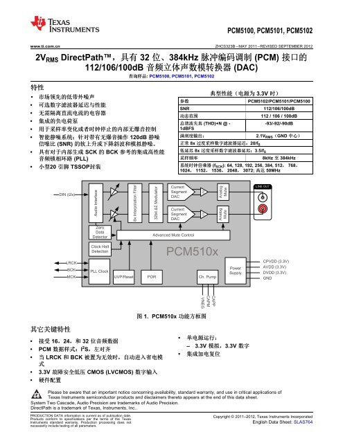
DIN (i2s)<br />
LRCK<br />
BCK<br />
MCK<br />
Audio Interface<br />
Zero<br />
Data<br />
Detector<br />
Clock Halt<br />
Detection<br />
PLL Clock<br />
UVP/Reset<br />
8x Interpolation Filter<br />
32bit ∆Σ Modulator<br />
POR<br />
Current<br />
Segment<br />
DAC<br />
Current<br />
Segment<br />
DAC<br />
Advanced Mute Control<br />
I/V I/V<br />
PCM510x<br />
Ch. Pump<br />
VNEG<br />
CAPP<br />
CAPM<br />
Analog<br />
Mute<br />
Analog<br />
Mute<br />
PCM5100, PCM5101, PCM5102<br />
www.ti.com.cn ZHCS323B –MAY 2011–REVISED SEPTEMBER 2012<br />
2V RMS DirectPath,具有 32 位、384kHz 脉冲编码调制 (PCM) 接口的<br />
112/106/100dB 音频立体声数模转换器 (DAC)<br />
查询样品: PCM5100, PCM5101, PCM5102<br />
1特性<br />
23• 市场领先的低带外噪声<br />
典型性能(电源为 3.3V 时)<br />
•<br />
•<br />
•<br />
可选数字滤波器延迟与性能<br />
无需隔离直流电流的电容器<br />
集成的负电荷泵<br />
参数<br />
SNR<br />
动态范围<br />
总谐波失真 (THD)+N @ -<br />
PCM5102/PCM5101/PCM5100<br />
112/106/100dB<br />
112 / 106 / 100dB<br />
-93/-92/-90dB<br />
• 用于采样率变化或者时钟停止的内部无爆音控制<br />
1dBFS<br />
• 智能静噪系统;针对带有无爆音操作 120dB 静噪 满刻度输出: 2.1VRMS(GND 中心)<br />
信噪比 (SNR) 的软上升或下降斜波和模拟静噪。 正常 8x 过度采样数字滤波器延迟:20/fS • 具有对于内部生成 SCK 的 BCK 参考的集成高性能 低延迟 8x 过度采样数字滤波器延迟:3.5/fS 音频锁相环路 (PLL)<br />
采样频率 8kHz 至 384kHz<br />
• 小型20 引脚 TSSOP封装<br />
系统时钟倍乘器 (fSCK): 64, 128, 192, 256, 384, 512, 768,<br />
1024, 1152, 1536, 2048, 3072; 高达 50MHz<br />
其它关键特性<br />
• 接受 16,24,和 32 位音频数据<br />
• PCM 数据样式:I2S,左对齐 • 当 LRCK 和 BCK 被置为无效时,自动进入省电模<br />
式<br />
• 3.3V 故障安全低压 CMOS (LVCMOS) 数字输入<br />
• 硬件配置<br />
1<br />
图 1. PCM510x 功能方框图<br />
Power<br />
Supply<br />
• 单电源运行:<br />
– 3.3V 模拟,3.3V 数字<br />
• 集成加电复位<br />
LINE OUT<br />
CPVDD (3.3V)<br />
AVDD (3.3V)<br />
DVDD (3.3V)<br />
GND<br />
Please be aware that an important notice concerning availability, standard warranty, and use in critical applications of<br />
Texas Instruments semiconductor products and disclaimers thereto appears at the end of this data sheet.<br />
2System Two Cascade, Audio Precision are trademarks of Audio Precision.<br />
3DirectPath is a trademark of Texas, Instruments, Inc..<br />
PRODUCTION DATA information is current as of publication date. Copyright © 2011–2012, Texas Instruments Incorporated<br />
Products conform to specifications per the terms of the Texas<br />
Instruments standard warranty. Production processing does not English Data Sheet: SLAS764<br />
necessarily include testing of all parameters.
PCM5100, PCM5101, PCM5102<br />
ZHCS323B –MAY 2011–REVISED SEPTEMBER 2012 www.ti.com.cn<br />
应用范围<br />
This integrated circuit can be damaged by ESD. Texas Instruments recommends that all integrated circuits be handled with<br />
appropriate precautions. Failure to observe proper handling and installation procedures can cause damage.<br />
ESD damage can range from subtle performance degradation to complete device failure. Precision integrated circuits may be more<br />
susceptible to damage because very small parametric changes could cause the device not to meet its published specifications.<br />
• A/V 接收器<br />
• DVD,BD 播放器<br />
• HDTV 接收器<br />
• 需要 2V RMS 音频输出的应用<br />
说明<br />
此PCM510x器件是单片 CMOS 集成电路系列产品,它包括一个立体声数模转换器和采用薄型小外形尺寸 (TSSOP)<br />
封装的附加支持电路。 PCM510x使用 TI 的高级分段 DAC 架构的最新一代产品来实现出色的动态性能并提升了对<br />
于时钟抖动的耐受度。<br />
PCM510x 提供了 2.1V RMS 接地中心输出,使得设计人员能够去除输出上的隔直电容器,以及与单电源线路驱动器<br />
相关的外部静噪电路。<br />
集成的线路驱动器通过支持低至 1kΩ 的负载从而在性能上超过所有其它基于电荷泵的线路驱动器。 通过支持低至<br />
1kΩ 的负载,PCM510x实际能够驱动多达 10 个并行产品,诸如 LCD TV,DVDR,AV 接收器和其它器件。<br />
器件上集成的 PLL 免除了对于系统时钟(通常称为主时钟)的需要,从而实现一个 3 线制 I 2 C 连接并减少了系统<br />
电磁干扰 (EMI)。<br />
智能时钟误差和功率感应欠压保护利用一个两级静噪系统实现无爆音性能。 发生时钟误差或者系统电源故障时,器<br />
件减弱数字数据(或者已知最后的正确数据),然后将模拟电路静噪。<br />
PCM510x系列产品提供比现有 DAC 技术最多低 20dB 的带外噪声,减少了下行放大器 / ADC 中的 EMI 和失<br />
真。(从一直使用的传统 100kHz 噪声倍频带 (OBN) 测量到 3MHz 测量)<br />
PCM510x 接受具有 16 至 32 位数据的工业标准音频数据格式。 支持高达 384kHz 的采样率。<br />
空白<br />
Table 1. PCM510x器件之间的差异<br />
部件号 动态范围 SNR THD<br />
PCM5102 112dB 112dB -93dB<br />
PCM5101 106dB 106dB -92dB<br />
PCM5100 100dB 100dB -90dB<br />
2 Copyright © 2011–2012, Texas Instruments Incorporated
PCM5100, PCM5101, PCM5102<br />
www.ti.com.cn ZHCS323B –MAY 2011–REVISED SEPTEMBER 2012<br />
This integrated circuit can be damaged by ESD. Texas Instruments recommends that all integrated circuits be handled with<br />
appropriate precautions. Failure to observe proper handling and installation procedures can cause damage.<br />
ESD damage can range from subtle performance degradation to complete device failure. Precision integrated circuits may be more<br />
susceptible to damage because very small parametric changes could cause the device not to meet its published specifications.<br />
TERMINAL FUNCTIONS, PCM510x<br />
TERMINAL<br />
NAME NO.<br />
DEVICE INFORMATION<br />
PCM510x (top view)<br />
Table 2. TERMINAL FUNCTIONS, PCM510x<br />
I/O DESCRIPTION<br />
CPVDD 1 — Charge pump power supply, 3.3V<br />
CAPP 2 O Charge pump flying capacitor terminal for positive rail<br />
CPGND 3 — Charge pump ground<br />
CAPM 4 O Charge pump flying capacitor terminal for negative rail<br />
VNEG 5 O Negative charge pump rail terminal for decoupling, -3.3V<br />
OUTL 6 O Analog output from DAC left channel<br />
OUTR 7 O Analog output from DAC right channel<br />
AVDD 8 -— Analog power supply, 3.3V<br />
AGND 9 — Analog ground<br />
DEMP 10 I De-emphasis control for 44.1kHz sampling rate (1) : Off (Low) / On (High)<br />
FLT 11 I Filter select : Normal latency (Low) / Low latency (High)<br />
SCK 12 I System clock input (1)<br />
BCK 13 I Audio data bit clock input (1)<br />
DIN 14 I Audio data input (1)<br />
LRCK 15 I Audio data word clock input (1)<br />
FMT 16 I Audio format selection : I 2 S (Low) / Left justified (High)<br />
XSMT 17 I Soft mute control (1) : Soft mute (Low) / soft un-mute (High)<br />
LDOO 18 — Internal logic supply rail terminal for decoupling<br />
DGND 19 — Digital ground<br />
DVDD 20 — Digital power supply, 3.3V<br />
(1) Failsafe LVCMOS Schmitt trigger input<br />
Copyright © 2011–2012, Texas Instruments Incorporated 3
PCM5100, PCM5101, PCM5102<br />
ZHCS323B –MAY 2011–REVISED SEPTEMBER 2012 www.ti.com.cn<br />
ABSOLUTE MAXIMUM RATINGS<br />
over operating free-air temperature range (unless otherwise noted)<br />
Supply Voltage AVDD, CPVDD, DVDD –0.3 to 3.9<br />
VALUE UNIT<br />
Digital Input Voltage –0.3 to 3.9 V<br />
Analog Input Voltage –0.3 to 3.9<br />
Operating Temperature Range –25 to 85<br />
Storage Temperature Range –65 to 150<br />
THERMAL CHARACTERISTICS<br />
over operating free-air temperature range (unless otherwise noted)<br />
PARAMETER TEST CONDITIONS MIN TYP MAX UNIT<br />
θ JA Theta JA High K 91.2<br />
ψ JT Psi JT 1.0<br />
ψ JB Psi JB 41.5 ºC/W<br />
θ JC Theta JC Top 25.3<br />
θ JB Theta JB 42.0<br />
ELECTRICAL CHARACTERISTICS<br />
All specifications at T A = 25°C, AV DD = CPV DD = DV DD = 3.3V, f S = 48kHz, system clock = 512 f S and 24-bit data unless<br />
otherwise noted.<br />
PARAMETER TEST CONDITIONS MIN TYP MAX UNIT<br />
Resolution 16 24 32 Bits<br />
Data Format (PCM Mode)<br />
Audio data interface format I 2 S, left justified<br />
Audio data bit length 16, 24, 32-bit acceptable<br />
Audio data format MSB First, 2’s Complement<br />
f S (1) Sampling frequency 8 384 kHz<br />
Digital Input/Output<br />
V IH<br />
V IL<br />
System clock frequency 64, 128, 192, 256, 384, 512, 768, 1024, 1152, 1536, 2048, or<br />
3072<br />
f SCK, up to 50Mhz<br />
Logic Family: 3.3V LVCMOS compatible<br />
0.7×DVDD Input logic level V<br />
0.3×DVDD I IH V IN = V DD 10<br />
Input logic current µA<br />
I IL V IN = 0V –10<br />
V OH I OH = –4mA 0.8×DV DD<br />
Output logic level V<br />
V OL I OL = 4mA 0.22×DV DD<br />
(1) One sample time si defined as the reciprocal of the sampling frequency. 1t S = 1/f S<br />
4 Copyright © 2011–2012, Texas Instruments Incorporated<br />
°C
PCM5100, PCM5101, PCM5102<br />
www.ti.com.cn ZHCS323B –MAY 2011–REVISED SEPTEMBER 2012<br />
ELECTRICAL CHARACTERISTICS (continued)<br />
All specifications at T A = 25°C, AV DD = CPV DD = DV DD = 3.3V, f S = 48kHz, system clock = 512 f S and 24-bit data unless<br />
otherwise noted.<br />
PARAMETER TEST CONDITIONS MIN TYP MAX UNIT<br />
Dynamic Performance (PCM Mode) (2)(3) (Values shown for three devices PCM5102/PCM5101/PCM5100)<br />
Analog Output<br />
THD+N at –1 dBFS (3)<br />
Dynamic range (3)<br />
Signal-to-noise ratio (3)<br />
f S = 48kHz –93/–92/–90 -83/ -82/ -80<br />
f S = 96kHz –93/–92/–90<br />
f S = 192kHz –93/–92/–90<br />
EIAJ, A-weighted, f S = 48kHz 106/ 100/ 95 112/106/100<br />
EIAJ, A-weighted, f S = 96kHz 112/106/100<br />
EIAJ, A-weighted, f S = 192kHz 112/106/100<br />
EIAJ, A-weighted, f S = 48kHz 112/106/100 dB<br />
EIAJ, A-weighted, f S = 96kHz 112/106/100<br />
EIAJ, A-weighted, f S = 192kHz 112/106/100<br />
Signal to noise ratio with EIAJ, A-weighted, f S = 48kHz 113 123<br />
analog mute (3)(4)<br />
EIAJ, A-weighted, f S = 96kHz 123<br />
EIAJ, A-weighted, f S = 192kHz 123<br />
Channel Separation f S = 48 kHz 100/ 95/ 90 109/103/97<br />
f S = 96kHz 109/103/97<br />
f S = 192kHz 109/103/97<br />
Output voltage 2.1 V RMS<br />
Gain error –6 ±2.0 6 % of FSR<br />
Gain mismatch, channel-to- –6 ±2.0 6 % of FSR<br />
channel<br />
Bipolar zero error At bipolar zero –5 ±1.0 5 mV<br />
Load impedance 1 kΩ<br />
Filter Characteristics–1: Normal<br />
Pass band 0.45f S<br />
Stop band 0.55f S<br />
Stop band attenuation –60<br />
Pass-band ripple ±0.02<br />
Delay time 20/f S s<br />
Filter Characteristics–2: Low Latency<br />
Pass band 0.47f S<br />
Stop band 0.55f S<br />
Stop band attenuation –52<br />
Pass-band ripple ±0.0001<br />
Delay time 3.5/f S s<br />
(2) Filter condition: THD+N: 20Hz HPF, 20kHz AES17 LPF Dynamic range: 20Hz HPF, 20kHz AES17 LPF, A-weighted Signal-to-noise<br />
ratio: 20Hz HPF, 20kHz AES17 LPF, A-weighted Channel separation: 20Hz HPF, 20kHz AES17 LPF Analog performance specifications<br />
are measured using the System Two Cascade audio measurement system by Audio Precision in the RMS mode.<br />
(3) Output load is 10kΩ, with 470Ω output resistor and a 2.2nF shunt capacitor (see recommended output filter).<br />
(4) Assert XSMT or both L-ch and R-ch PCM data are BPZ<br />
Copyright © 2011–2012, Texas Instruments Incorporated 5<br />
dB<br />
dB
PCM5100, PCM5101, PCM5102<br />
ZHCS323B –MAY 2011–REVISED SEPTEMBER 2012 www.ti.com.cn<br />
ELECTRICAL CHARACTERISTICS (continued)<br />
All specifications at T A = 25°C, AV DD = CPV DD = DV DD = 3.3V, f S = 48kHz, system clock = 512 f S and 24-bit data unless<br />
otherwise noted.<br />
PARAMETER TEST CONDITIONS MIN TYP MAX UNIT<br />
Power Supply Requirements<br />
DV DD Digital supply voltage Target DV DD = 3.3V 3.0 3.3 3.6<br />
AV DD Analog supply voltage 3.0 3.3 3.6 VDC<br />
CPV DD Charge-pump suply voltage 3.0 3.3 3.6<br />
I DD<br />
I DD<br />
I DD<br />
DV DD supply current at 3.3V (5)<br />
DV DD supply current at 3.3V (6)<br />
DV DD supply current at 3.3V (7)<br />
f S = 48kHz 7 12<br />
f S = 96kHz 8 mA<br />
f S = 192kHz 9<br />
f S = 48kHz 8 13<br />
f S = 96kHz 9 mA<br />
f S = 192kHz 10<br />
0.5 0.8 mA<br />
fS = 48kHz 11 16<br />
ICC AVDD / CPVDD Supply<br />
Current<br />
fS = 96kHz 11 mA<br />
(5)<br />
fS = 192kHz 11<br />
fS = 48kHz 22 32<br />
ICC AVDD / CPVDD Supply<br />
Current<br />
fS = 96kHz 22 mA<br />
(6)<br />
fS = 192kHz 22<br />
I CC<br />
AVDD / CPVDD Supply fS = n/a 0.2 0.4<br />
Current (7)<br />
Power Dissipation, DVDD =<br />
3.3V (5)<br />
Power Dissipation, DVDD =<br />
3.3V (6)<br />
f S = 48kHz 59.4 92.4<br />
f S = 96kHz 62.7 mW<br />
f S = 192kHz 66.0<br />
f S = 48kHz 99.0 148.5<br />
f S = 96kHz 102.3 mW<br />
f S = 192kHz 105.6<br />
Power Dissipation, DVDD = fS = n/a (Power Down Mode) 2.3 4.0<br />
3.3V (7)<br />
(5) Input is Bipolar Zero data.<br />
(6) Input is 1kHz -1dBFS data<br />
(7) Power Down Mode<br />
6 Copyright © 2011–2012, Texas Instruments Incorporated<br />
mA<br />
mW
THD+N [dB]<br />
10<br />
-10<br />
-30<br />
-50<br />
-70<br />
-90<br />
-110<br />
PCM5100 THD+N PCM5101 THD+N<br />
vs vs<br />
Input Level Input Level<br />
10<br />
-100 -80 -60 -40 -20 0<br />
Input Level [dBFS]<br />
THD+N [dB]<br />
10<br />
-10<br />
-30<br />
-50<br />
-70<br />
-90<br />
-110<br />
-110<br />
-100 -80 -60 -40 -20 0<br />
Input Level [dBFS]<br />
THD+N [dB]<br />
-10<br />
-30<br />
-50<br />
-70<br />
-90<br />
PCM5100, PCM5101, PCM5102<br />
www.ti.com.cn ZHCS323B –MAY 2011–REVISED SEPTEMBER 2012<br />
TYPICAL CHARACTERISTICS<br />
All specifications at T A = 25°C, AV DD = CPV DD = DV DD = 3.3V, f S = 48kHz, system clock = 512 f S and 24-bit data unless<br />
otherwise noted.<br />
-100 -80 -60 -40 -20 0<br />
Input Level [dBFS]<br />
Figure 2. Figure 3.<br />
PCM5102 THD+N<br />
vs<br />
Input Level<br />
Figure 4.<br />
Copyright © 2011–2012, Texas Instruments Incorporated 7
PCM5100, PCM5101, PCM5102<br />
ZHCS323B –MAY 2011–REVISED SEPTEMBER 2012 www.ti.com.cn<br />
TYPICAL CHARACTERISTICS (continued)<br />
All specifications at T A = 25°C, AV DD = CPV DD = DV DD = 3.3V, f S = 48kHz, system clock = 512 f S and 24-bit data unless<br />
otherwise noted.<br />
Amplitude [dB]<br />
-20<br />
-40<br />
-60<br />
-80<br />
-100<br />
-120<br />
-140<br />
-160<br />
-180<br />
PCM5100 FFT Plot at BPZ With AMUTE PCM5101 FFT Plot at BPZ With AMUTE<br />
-20<br />
0 5 10 15 20<br />
Frequency [kHz]<br />
Amplitude [dB]<br />
-20<br />
-40<br />
-60<br />
-80<br />
-100<br />
-120<br />
-140<br />
-160<br />
-180<br />
Amplitude [dB]<br />
-40<br />
-60<br />
-80<br />
-100<br />
-120<br />
-140<br />
-160<br />
-180<br />
0 5 10 15 20<br />
Frequency [kHz]<br />
0 5 10 15 20<br />
Frequency [kHz]<br />
Figure 5. Figure 6.<br />
PCM5102 FFT Plot at BPZ With AMUTE<br />
Figure 7.<br />
8 Copyright © 2011–2012, Texas Instruments Incorporated
Amplitude [dB]<br />
0<br />
-20<br />
-40<br />
-60<br />
-80<br />
-100<br />
-120<br />
-140<br />
-160<br />
PCM5100 FFT Plot at –60dB To 300kHz PCM5101 FFT Plot at –60dB To 300kHz<br />
0<br />
0 50 100 150 200 250 300<br />
Frequency [kHz]<br />
Amplitude [dB]<br />
0<br />
-20<br />
-40<br />
-60<br />
-80<br />
-100<br />
-120<br />
-140<br />
-160<br />
Amplitude [dB]<br />
-20<br />
-40<br />
-60<br />
-80<br />
-100<br />
-120<br />
-140<br />
-160<br />
0 50 100 150 200 250 300<br />
Frequency [kHz]<br />
PCM5100, PCM5101, PCM5102<br />
www.ti.com.cn ZHCS323B –MAY 2011–REVISED SEPTEMBER 2012<br />
TYPICAL CHARACTERISTICS (continued)<br />
All specifications at T A = 25°C, AV DD = CPV DD = DV DD = 3.3V, f S = 48kHz, system clock = 512 f S and 24-bit data unless<br />
otherwise noted.<br />
0 50 100 150 200 250 300<br />
Frequency [kHz]<br />
Figure 8. Figure 9.<br />
PCM5102 FFT Plot at –60dB To 300kHz<br />
Figure 10.<br />
Copyright © 2011–2012, Texas Instruments Incorporated 9
PCM5100, PCM5101, PCM5102<br />
ZHCS323B –MAY 2011–REVISED SEPTEMBER 2012 www.ti.com.cn<br />
Reset and System Clock Functions<br />
Power-On Reset Function<br />
AVVDD, DVVDD,<br />
CPVVDD<br />
Inteernaal Reeseet<br />
3.3VV<br />
2.8VV<br />
I 2 S Cloccks<br />
SCK, BCK, LRCK<br />
APPLICATION INFORMATION<br />
The PCM510x includes a power-on reset function shown in Figure 11. With V DD > 2.8V, the power-on reset<br />
function is enabled. After the initialization period, the PCM510x is set to its default reset state.<br />
Inteernaal Reeseet<br />
4 ms<br />
Figure 11. Power-On Reset Timing, DVDD = 3.3V<br />
Reeseet Reemovvaal<br />
10 Copyright © 2011–2012, Texas Instruments Incorporated
System Clock<br />
(SCK)<br />
"H"<br />
"L"<br />
tSCKL<br />
tSCKH<br />
tSCY<br />
PCM5100, PCM5101, PCM5102<br />
www.ti.com.cn ZHCS323B –MAY 2011–REVISED SEPTEMBER 2012<br />
System Clock Input<br />
The PCM510x requires a system clock to operate the digital interpolation filters and advanced segment DAC<br />
modulators. The system clock is applied at the SCK input (pin 12) and supports up to 50MHz. The PCM510x<br />
system-clock detection circuit automatically senses the system-clock frequency. Common audio sampling<br />
frequencies of 8kHz, 16kHz, 32kHz - 44.1kHz - 48kHz, 88.2kHz - 96kHz, 176.4kHz -192kHz, and 384kHz with<br />
±4% tolerance are supported. The sampling frequency detector sets the clock for the digital filter, Delta Sigma<br />
Modulator (DSM) and the Negative Charge Pump (NCP) automatically. Table 3 shows examples of system clock<br />
frequencies for common audio sampling rates.<br />
SCK rates that are not common to standard audio clocks, between 1MHz and 50MHz, are only supported in<br />
software mode, available only in the PCM512x and PCM514x devices, by configuring various PLL and clockdivider<br />
registers. Software mode allows the device to become a clock master and drive the host serial port with<br />
LRCK and BCK, from a non-audio related clock; for example, using 12MHz to generate 44.1kHz (LRCK) and<br />
2.8224MHz (BCK).<br />
Figure 12 shows the timing requirements for the system clock input. For optimal performance, it is important to<br />
use a clock source with low phase jitter and noise.<br />
Table 3. System Master Clock Inputs for Audio Related Clocks<br />
Sampling<br />
System Clock Frequency (fSCK) (MHz)<br />
Frequency 64 fS 128 fS 192 fS 256 fS 384 fS 512 fS 768 fS 1024 fS 1152 fS 1536 fS 2048 fS 3072 fS 8 kHz – (1)<br />
16 kHz – (1)<br />
32 kHz – (1)<br />
44.1 kHz – (1)<br />
48 kHz – (1)<br />
88.2 kHz – (1)<br />
96 kHz – (1)<br />
176.4 kHz – (1)<br />
192 kHz – (1)<br />
1.0240 (2)<br />
2.0480 (2)<br />
4.0960 (2)<br />
5.6488 (2)<br />
6.1440 (2)<br />
11.2896 (2)<br />
12.2880 (2)<br />
1.5360 (2)<br />
3.0720 (2)<br />
6.1440 (2)<br />
8.4672 (2)<br />
9.2160 (2)<br />
384 kHz 24.5760 49.1520 – (1)<br />
2.0480 3.0720 4.0960 6.1440 8.1920 9.2160 12.2880 16.3840 24.5760<br />
4.0960 6.1440 8.1920 12.2880 16.3840 18.4320 24.5760 36.8640 49.1520<br />
8.1920 12.2880 16.3840 24.5760 32.7680 36.8640 49.1520 – (1)<br />
11.2896 16.9344 22.5792 33.8688 45.1584 – (1)<br />
12.2880 18.4320 24.5760 36.8640 49.1520 – (1)<br />
16.9344 22.5792 33.8688 45.1584 – (1)<br />
18.4320 24.5760 36.8640 49.1520 – (1)<br />
22.5792 33.8688 45.1584 – (1)<br />
24.5760 36.8640 49.1520 – (1)<br />
(1) This system clock rate is not supported for the given sampling frequency.<br />
(2) This system clock rate is supported by PLL mode.<br />
– (1)<br />
– (1)<br />
– (1)<br />
– (1)<br />
– (1)<br />
Figure 12. Timing Requirements for SCK Input<br />
Table 4. Timing Requirements for SCK Input<br />
Parameters Min Max Unit<br />
t SCY System clock pulse cycle time 20 1000 ns<br />
t SCKH System clock pulse width, High 9 ns<br />
t SCKL System clock pulse width, Low 9 ns<br />
– (1)<br />
– (1)<br />
– (1)<br />
– (1)<br />
– (1)<br />
– (1)<br />
– (1)<br />
– (1)<br />
– (1)<br />
– (1)<br />
– (1)<br />
– (1)<br />
– (1)<br />
– (1)<br />
– (1)<br />
– (1)<br />
– (1)<br />
– (1)<br />
– (1)<br />
– (1)<br />
– (1)<br />
– (1)<br />
– (1)<br />
– (1)<br />
– (1)<br />
– (1)<br />
– (1)<br />
0.7*DVDD<br />
0.3*DVDD<br />
Copyright © 2011–2012, Texas Instruments Incorporated 11<br />
– (1)<br />
– (1)<br />
– (1)<br />
– (1)<br />
– (1)<br />
– (1)<br />
– (1)<br />
– (1)
PCM5100, PCM5101, PCM5102<br />
ZHCS323B –MAY 2011–REVISED SEPTEMBER 2012 www.ti.com.cn<br />
System Clock PLL Mode<br />
The system clock PLL mode allows designers to use a simple 3-wire I 2 S audio source when driving the DAC.<br />
The 3-wire source reduces the need for a high frequency SCK, making PCB layout easier, and reduces high<br />
frequency electromagnetic interference.<br />
The device starts up expecting an external SCK input, but if BCK and LRCK start correctly while SCK remains at<br />
ground level for 16 successive LRCK periods, then the internal PLL starts, automatically generating an internal<br />
SCK from the BCK reference. The PCM510x disables the internal PLL when an external SCK is supplied;<br />
specific BCK rates are required to generate an appropriate master clock. Table 5 describes the minimum and<br />
maximum BCK per LRCK for the integrated PLL to automatically generate an internal SCK.<br />
Audio Data Interface<br />
Audio Serial Interface<br />
Table 5. BCK Rates (MHz) by LRCK Sample Rate for<br />
PCM510x PLL Operation<br />
BCK (f S)<br />
Sample f (kHz) 32 64<br />
8 - -<br />
16 - 1.024<br />
32 1.024 2.048<br />
44.1 1.4112 2.8224<br />
48 1.536 3.072<br />
96 3.072 6.144<br />
192 6.144 12.288<br />
384 12.288 24.576<br />
The audio interface port is a 3-wire serial port, including LRCK (pin 15), BCK (pin 13), and DIN (pin 14). BCK is<br />
the serial audio bit clock, used to clock the serial data present on DIN into the serial shift register of the audio<br />
interface. Serial data is clocked into the PCM510x on the rising edge of BCK. LRCK is the serial audio left/right<br />
word clock.<br />
Table 6. PCM510x Audio Data Formats, Bit Depths and Clock Rates<br />
MAX LRCK<br />
CONTROL MODE FORMAT DATA BITS SCK RATE [x f S] BCK RATE [x f S]<br />
FREQUENCY [f S]<br />
Hardware Control I 2 S/LJ 32, 24, 20, 16<br />
128 – 3072<br />
Up to 192kHz 64, 48, 32<br />
(≤50MHz)<br />
384kHz 64, 128 64, 48, 32<br />
The PCM510x requires the synchronization of LRCK and system clock, but does not need a specific phase<br />
relation between LRCK and system clock.<br />
If the relationship between LRCK and system clock changes more than ±5 SCK, internal operation is initialized<br />
within one sample period and analog outputs are forced to the bipolar zero level until resynchronization between<br />
LRCK and system clock is completed.<br />
If the relationship between LRCK and BCK are invalid more than 4 LRCK periods, internal operation is initialized<br />
within one sample period and analog outputs are forced to the bipolar zero level until resynchronization between<br />
LRCK and BCK is completed.<br />
12 Copyright © 2011–2012, Texas Instruments Incorporated
LRCK<br />
(Input)<br />
BCK<br />
(Input)<br />
DATA<br />
(Input)<br />
tBCH<br />
tBCY<br />
tBCL<br />
tDS<br />
tBL<br />
tDH<br />
tLB<br />
PCM5100, PCM5101, PCM5102<br />
www.ti.com.cn ZHCS323B –MAY 2011–REVISED SEPTEMBER 2012<br />
PCM Audio Data Formats and Timing<br />
The PCM510x supports industry-standard audio data formats, including standard I 2 S and left-justified. Data<br />
formats are selected using the FMT (pin 16), Low for I 2 S, and High for Left-justified.<br />
All formats require binary 2s complement, MSB-first audio data. Figure 13 shows a detailed timing diagram for<br />
the serial audio interface.<br />
Figure 13. PCM510x Serial Audio Timing - Slave<br />
Table 7. Audio Interface Slave Timing<br />
Parameters Min Max Units<br />
t BCY BCK Pulse Cycle Time 40 ns<br />
t BCL BCK Pulse Width LOW 16 ns<br />
t BCH BCK Pulse Width HIGH 16 ns<br />
t BL BCK Rising Edge to LRCK Edge 8 ns<br />
t LB LRCK Edge to BCK Rising Edge 8 ns<br />
t DS DATA Set Up Time 8 ns<br />
t DH DATA Hold Time 8 ns<br />
f BCK BCK frequency @ DVDD=3.3V 24.576 MHz<br />
0. 5 * DVDD<br />
0. 5 * DVDD<br />
0. 5 * DVDD<br />
Copyright © 2011–2012, Texas Instruments Incorporated 13
PCM5100, PCM5101, PCM5102<br />
ZHCS323B –MAY 2011–REVISED SEPTEMBER 2012 www.ti.com.cn<br />
LRCK<br />
BCK<br />
DATA<br />
LRCK<br />
BCK<br />
Audio data word = 16-bit, BCK = 32, 48, 64fS<br />
DATA<br />
Audio data word = 24-bit, BCK = 48, 64fS<br />
DATA<br />
Audio data word = 32-bit, BCK = 64fS<br />
DATA<br />
L- channel R- channel<br />
1 2<br />
15 16<br />
1 2<br />
15 16<br />
1<br />
L-channel<br />
Audio data word = 16-bit, BCK = 32, 48, 64fS<br />
MSB LSB MSB LSB<br />
2 23 24<br />
1 2<br />
23 24<br />
MSB LSB MSB LSB<br />
1tS<br />
R-channel<br />
1 2<br />
15 16<br />
1 2<br />
15 16<br />
Audio data word = 24-bit, BCK = 48, 64fS<br />
- ,<br />
DATA<br />
Audio data word = 32-bit, BCK = 64fS<br />
DATA<br />
MSB LSB MSB LSB<br />
1 2<br />
2 24<br />
1 2<br />
23 24<br />
1tS<br />
MSB LSB MSB<br />
1 2<br />
31 32 1 2<br />
31 32<br />
MSB LSB MSB LSB<br />
Left Justified Data Format; L-channel = HIGH, R-channel = LOW<br />
1 2<br />
31 32 1 2<br />
31 32<br />
MSB LSB MSB LSB<br />
I 2 S Data Format; L-channel = LOW, R-channel = HIGH<br />
Figure 14. Left Justified Audio Data Format<br />
Figure 15. I 2 S Audio Data Format<br />
14 Copyright © 2011–2012, Texas Instruments Incorporated<br />
LSB
Amplitude (dB)<br />
0<br />
−20<br />
−40<br />
−60<br />
−80<br />
−100<br />
−120<br />
0 1 2<br />
Frequency (x fS) 3 4<br />
G012<br />
Amplitude (FFS)<br />
1.0<br />
0.8<br />
0.6<br />
0.4<br />
0.2<br />
0.0<br />
−0.2<br />
−0.4<br />
PCM5100, PCM5101, PCM5102<br />
www.ti.com.cn ZHCS323B –MAY 2011–REVISED SEPTEMBER 2012<br />
Function Descriptions<br />
Interpolation Filter<br />
The PCM510x provides 2 types of interpolation filter. Users can select which filter to use by using the FLT pin<br />
(pin11)<br />
Table 8. Digital Interpolation Filter Options<br />
FLT Pin Description<br />
0 FIR Normal x8/x4/x2/x1 Interpolation Filters<br />
1 IIR Low Latency x8/x4/x2/x1 Interpolation Filters<br />
The Normal x8/x4/x2/x1(bypass) Interpolation filter is programmed in 256 cycles in 1 sample time (t S) for sample<br />
rates from 8kHz to 384kHz.<br />
Table 9. Normal x8 Interpolation Filter<br />
Parameter Condition Value (Typ) Value (Max) Units<br />
Filter Gain Pass Band 0 ……. 0.45f S ±0.02 dB<br />
Filter Gain Stop Band 0.55f S ….. 7.455f S –60 dB<br />
Filter Group Delay 22t S s<br />
0 50 100 150 200 250 300 350 400<br />
Samples<br />
Figure 16. Normal x8 Interpolation Filter Frequency Figure 17. Normal x8 Interpolation Filter Impulse<br />
Response Response<br />
Copyright © 2011–2012, Texas Instruments Incorporated 15<br />
G023
PCM5100, PCM5101, PCM5102<br />
ZHCS323B –MAY 2011–REVISED SEPTEMBER 2012 www.ti.com.cn<br />
Amplitude (dB)<br />
0.05<br />
0.04<br />
0.03<br />
0.02<br />
0.01<br />
0.00<br />
−0.01<br />
−0.02<br />
−0.03<br />
−0.04<br />
−0.05<br />
0.0 0.1 0.2 0.3 0.4 0.5<br />
Frequency (x fS) Figure 18. Normal x8 Interpolation Filter Passband Ripple<br />
16 Copyright © 2011–2012, Texas Instruments Incorporated<br />
G034
Amplitude (dB)<br />
0<br />
−20<br />
−40<br />
−60<br />
−80<br />
−100<br />
−120<br />
0 1 2<br />
Frequency (x fS) 3 4<br />
Amplitude (dB)<br />
0.05<br />
0.04<br />
0.03<br />
0.02<br />
0.01<br />
0.00<br />
−0.01<br />
−0.02<br />
−0.03<br />
−0.04<br />
G009<br />
−0.05<br />
0.0 0.5<br />
Frequency (x fS) 1.0<br />
Amplitude (FFS)<br />
1.0<br />
0.8<br />
0.6<br />
0.4<br />
0.2<br />
0.0<br />
−0.2<br />
−0.4<br />
PCM5100, PCM5101, PCM5102<br />
www.ti.com.cn ZHCS323B –MAY 2011–REVISED SEPTEMBER 2012<br />
The Normal x4/x2/x1(bypass) Interpolation filter is programmed in 256 cycles in 1 sample time (t S) for sample<br />
rates from 8kHz to 384kHz.<br />
Table 10. Normal x4 Interpolation Filter<br />
Parameter Condition Value (Typ) Value (Max) Units<br />
Filter Gain Pass Band 0 ……. 0.45f S ±0.02 dB<br />
Filter Gain Stop Band 0.55f S ….. 7.455f S –60 dB<br />
Filter Group Delay 22t S s<br />
0 20 40 60 80 100 120 140 160<br />
Samples<br />
Figure 19. Normal x4 Interpolation Filter Frequency Figure 20. Normal x4 Interpolation Filter Impulse<br />
Response Response<br />
Figure 21. Normal x4 Interpolation Filter Passband Ripple<br />
Copyright © 2011–2012, Texas Instruments Incorporated 17<br />
G031<br />
G020
PCM5100, PCM5101, PCM5102<br />
ZHCS323B –MAY 2011–REVISED SEPTEMBER 2012 www.ti.com.cn<br />
Normal x2 / x1(bypass) Interpolation filter is programmed in 256 cycles in 1 sample time (t S) for sample rates<br />
from 8kHz to 384kHz.<br />
Amplitude (dB)<br />
0<br />
−20<br />
−40<br />
−60<br />
−80<br />
−100<br />
−120<br />
0 1 2<br />
Frequency (x fS) 3 4<br />
Amplitude (dB)<br />
0.05<br />
0.04<br />
0.03<br />
0.02<br />
0.01<br />
0.00<br />
−0.01<br />
−0.02<br />
−0.03<br />
−0.04<br />
Table 11. Normal x2 Interpolation Filter<br />
Parameter Condition Value (Typ) Value (Max) Units<br />
Filter Gain Pass Band 0 ……. 0.45f S ±0.02 dB<br />
Filter Gain Stop Band 0.55f S ….. 7.455f S –60 dB<br />
Filter Group Delay 22t S s<br />
G006<br />
−0.2<br />
−0.4<br />
−0.05<br />
0.0 0.5 1.0<br />
Frequency (x fS) 1.5 2.0<br />
Amplitude (FFS)<br />
1.0<br />
0.8<br />
0.6<br />
0.4<br />
0.2<br />
0.0<br />
0 10 20 30 40 50 60 70 80 90 100<br />
Samples<br />
Figure 22. Normal x2 Interpolation Filter Frequency Figure 23. Normal x2 Interpolation Filter Impulse<br />
Response Response<br />
Figure 24. Normal x2 Interpolation Filter Passband Ripple<br />
18 Copyright © 2011–2012, Texas Instruments Incorporated<br />
G028<br />
G017
Amplitude (dB)<br />
0<br />
−20<br />
−40<br />
−60<br />
−80<br />
−100<br />
−120<br />
0 1 2<br />
Frequency (x fS) 3 4<br />
Amplitude (dB)<br />
0.00010<br />
0.00008<br />
0.00006<br />
0.00004<br />
0.00002<br />
0.00000<br />
−0.00002<br />
−0.00004<br />
−0.00006<br />
−0.00008<br />
G011<br />
−0.00010<br />
0.0 0.1 0.2 0.3 0.4 0.5<br />
Frequency (x fS) Amplitude (FFS)<br />
1.0<br />
0.8<br />
0.6<br />
0.4<br />
0.2<br />
0.0<br />
−0.2<br />
−0.4<br />
−0.6<br />
PCM5100, PCM5101, PCM5102<br />
www.ti.com.cn ZHCS323B –MAY 2011–REVISED SEPTEMBER 2012<br />
The low-latency x8 / x4 / x2 / x1(bypass) Interpolation filter is programmed in 256 cycles 1 sample time (t S) for<br />
sample rates from 8kHz to 384kHz.<br />
Table 12. Low latency x8 Interpolation Filter<br />
Parameter Condition Value (Typ) Units<br />
Filter Gain Pass Band 0 ……. 0.45f S ±0.0001 dB<br />
Filter Gain Stop Band 0.55f S ….. 7.455f S –52 dB<br />
Filter Group Delay 3.5t S s<br />
0 50 100 150 200 250 300 350 400<br />
Samples<br />
Figure 25. Low latency x8 Interpolation Filter Figure 26. Low latency x8 Interpolation Filter<br />
Frequency Response Impulse Response<br />
Figure 27. Low latency x8 Interpolation Filter Passband Ripple<br />
Copyright © 2011–2012, Texas Instruments Incorporated 19<br />
G033<br />
G022
PCM5100, PCM5101, PCM5102<br />
ZHCS323B –MAY 2011–REVISED SEPTEMBER 2012 www.ti.com.cn<br />
Amplitude (dB)<br />
0<br />
−20<br />
−40<br />
−60<br />
−80<br />
−100<br />
−120<br />
0 1 2<br />
Frequency (x fS) 3 4<br />
Amplitude (dB)<br />
Table 13. Low latency x4 Interpolation Filter<br />
Parameter Condition Value (Typ) Units<br />
Filter Gain Pass Band 0 ……. 0.45f S ±0.0001 dB<br />
Filter Gain Stop Band 0.55f S ….. 3.455f S –52 dB<br />
Filter Group Delay 3.5t S s<br />
0.0001<br />
0.00008<br />
0.00006<br />
0.00004<br />
0.00002<br />
0<br />
−0.00002<br />
−0.00004<br />
−0.00006<br />
−0.00008<br />
G008<br />
−0.2<br />
−0.4<br />
−0.6<br />
−0.0001<br />
0.0 0.5<br />
Frequency (x fS) 1.0<br />
Amplitude (FFS)<br />
1.0<br />
0.8<br />
0.6<br />
0.4<br />
0.2<br />
0.0<br />
0 20 40 60 80 100 120 140 160 180<br />
Samples<br />
Figure 28. Low latency x4 Interpolation Filter Figure 29. Low latency x4 Interpolation Filter<br />
Frequency Response Impulse Response<br />
Figure 30. Low latency x4 Interpolation Filter Passband Ripple<br />
20 Copyright © 2011–2012, Texas Instruments Incorporated<br />
G030<br />
G019
Amplitude (dB)<br />
0<br />
−20<br />
−40<br />
−60<br />
−80<br />
−100<br />
−120<br />
0 1 2<br />
Frequency (x fS) 3 4<br />
Amplitude (dB)<br />
0.0001<br />
0.00008<br />
0.00006<br />
0.00004<br />
0.00002<br />
0<br />
−0.00002<br />
−0.00004<br />
−0.00006<br />
−0.00008<br />
G005<br />
−0.0001<br />
0.0 0.5<br />
Frequency (x fS) 1.0<br />
Amplitude (FFS)<br />
1.0<br />
0.8<br />
0.6<br />
0.4<br />
0.2<br />
0.0<br />
−0.2<br />
−0.4<br />
PCM5100, PCM5101, PCM5102<br />
www.ti.com.cn ZHCS323B –MAY 2011–REVISED SEPTEMBER 2012<br />
space<br />
Table 14. Low latency x2 Interpolation Filter<br />
Parameter Condition Value (Typ) Units<br />
Filter Gain Pass Band 0 ……. 0.45f S ±0.0001 dB<br />
Filter Gain Stop Band 0.55f S ….. 1.455f S –52 dB<br />
Filter Group Delay 3.5t S s<br />
0 10 20 30 40 50 60 70 80 90 100<br />
Samples<br />
Figure 31. Low latency x2 Interpolation Filter Figure 32. Low latency x2 Interpolation Filter<br />
Frequency Response Impulse Response<br />
Figure 33. Low latency x2 Interpolation Filter Passband Ripple<br />
Copyright © 2011–2012, Texas Instruments Incorporated 21<br />
G030<br />
G016
PCM5100, PCM5101, PCM5102<br />
ZHCS323B –MAY 2011–REVISED SEPTEMBER 2012 www.ti.com.cn<br />
Zero Data Detect<br />
The PCM510x has a zero-data detect function. When the device detects continuous zero data, it enters a full<br />
analog mute condition.<br />
The PCM510x counts zero data over 1024LRCKs (21ms @ 48kHz) before setting analog mute.<br />
Power Save Mode<br />
When any kind of clock error (SCK, BCK, and LRCK) or clock halt is detected, the PCM510x enters Stand-by<br />
mode automatically. The current-segment DAC and Line driver are also powered down.<br />
When BCK and LRCK halt to a low level for more than 1 second, the PCM510x enters Power down mode<br />
automatically. Power-down mode includes the negative charge pump and Bias/Reference circuit power-down in<br />
addition to stand-by.<br />
Whenever expected Audio clocks (SCK, BCK, LRCK) are applied to the PCM510x, the device starts its powerup<br />
sequence automatically.<br />
XSMT Pin (Soft Mute and Soft Un-Mute)<br />
For external digital control of the PCM510x, the XSMT pin must be driven by an external digital host with a<br />
specific/minimum rise time (t r) and fall time (t f) for soft mute and soft un-mute. The PCM510x requires t r/t f times<br />
of less than 20ns. In the majority of applications, this shouldn’t be a problem, however, traces with high<br />
capacitance may have issues.<br />
When the XSMT pin is shifted from high to low (3.3V to 0V), a soft digital attenuation ramp is started. –1dB<br />
attenuation will be applied every 1t S from 0dBFS to –∞. This attenuation takes 104 sample times.<br />
When the XSMT pin is shifted from low to high (0V to 3.3V), a soft digital “un-mute” is started. 1dB gain steps are<br />
applied every t S from –∞ to 0dBFS. This ramp-up takes 104 sample times.<br />
XSMT<br />
tr tf<br />
XSMT<br />
tf<br />
System<br />
VDD<br />
12V<br />
supply<br />
7.25k�<br />
XSMT<br />
2.75k�<br />
Digital Attenuation Followed by Analog Mute<br />
Analog Mute<br />
PCM5100, PCM5101, PCM5102<br />
www.ti.com.cn ZHCS323B –MAY 2011–REVISED SEPTEMBER 2012<br />
External Power Sense Undervoltage Protection mode (supported only when DVDD = 3.3V)<br />
The XSMT pin can also be used to monitor a system voltage, such as the 24VDC LCD TV backlight, or 12VDC<br />
system supply using a potential divider created with two resistors. (See Figure 35 )<br />
• If the XSMT pin makes a transition from 1 to 0 over 6ms or more, the device will switch into external undervoltage<br />
protection mode. In this mode, two trigger levels are used.<br />
• When XSMT pin level reaches 2V, soft mute process begins.<br />
• When XSMT pin level reaches 1.2V, analog mute will engage, regardless of digital audio level, and analog<br />
shut down will begin. (For example, DAC circuitry powers down).<br />
A timing diagram to show this is shown in Figure 36.<br />
NOTE<br />
The XSMT input pins voltage range is from –0.3V to DVDD + 0.3V.The ratio of external<br />
resistors must be considered within this input range. Any increase in power supply (such<br />
as power supply positive noise/ripple) can pull the XSMT pin higher than DVDD+0.3V.<br />
For example, if the PCM510x is monitoring a 12V input, and dividing the voltage by 4, then the voltage at XSMT<br />
during ideal power supply conditions will be 3V. If the voltage spikes any higher than 14.4V, then XSMT will see<br />
a voltage in excess of 3.6V (DVDD+0.3), potentially damaging the device.<br />
Providing the divider is set appropriately, any DC voltage can be monitored.<br />
Figure 35. XSMT in External UVP Mode<br />
Figure 36. XSMT Timing for Undervoltage Protection<br />
2.0 V<br />
1.2 V<br />
0.9 * DVDD<br />
0.1 * DVDD<br />
Copyright © 2011–2012, Texas Instruments Incorporated 23
PCM5100, PCM5101, PCM5102<br />
ZHCS323B –MAY 2011–REVISED SEPTEMBER 2012 www.ti.com.cn<br />
Recommended Powerdown Sequence<br />
With inadequate system design, the PCM510x can exhibit some pop on power down. Pops are caused by the<br />
device not having enough time to detect power loss and start the muting process.<br />
The PCM510x evaluation board avoids audible pop with an electrolytic decoupling capacitor. This capacitor<br />
provides enough time between data loss from USB or S/PDIF and power supply loss for the muting process to<br />
take place.<br />
The PCM510x has two auto-mute functions to mute the device upon power loss (intentional or unintentional).<br />
XSMT = 0<br />
When the XSMT pin is pulled low, the incoming PCM data is attenuated to 0, closely followed by a hard analog<br />
mute. This process takes 150 sample times (t s) + 0.2mS.<br />
As this mute time is mainly dominated by the sampling frequency, systems sampling at 192kHz will mute much<br />
faster than a 48kHz system.<br />
Clock Error Detect<br />
When clock error is detected on the incoming data clock, the PCM510x family switches to an internal oscillator,<br />
and continues to the drive the DAC, while attenuating the data from the last known value. Once this process is<br />
complete, the PCM510x outputs will be hard muted to ground.<br />
Planned Shutdown<br />
These auto-muting processes can be manipulated by system designs to mute before power loss in the following<br />
ways:<br />
1. Assert XSMT low 150t S + 0.2mS before power is removed.<br />
VDD<br />
XSMT<br />
3.3V<br />
0V<br />
High<br />
Low<br />
High<br />
I 2 S Clocks<br />
SCK, BCK, LRCK<br />
Low<br />
Time<br />
150t + 0.2ms<br />
S<br />
24 Copyright © 2011–2012, Texas Instruments Incorporated
110V / 220V<br />
VDD<br />
XSMT<br />
3.3V<br />
0V<br />
High<br />
Low<br />
High<br />
I2S Clocks<br />
SCK, BCK, LRCK<br />
Low<br />
SMPS<br />
6V<br />
MCU GPIO “mute” signal<br />
10 F<br />
Time<br />
Linear<br />
Regulator<br />
3msec<br />
3V3<br />
GND GND<br />
PCM5100, PCM5101, PCM5102<br />
www.ti.com.cn ZHCS323B –MAY 2011–REVISED SEPTEMBER 2012<br />
2. Stop I 2 S clocks (SCK, BCK, LRCK) 3ms before powerdown as shown below:<br />
Unplanned Shutdown<br />
Many systems use a low-noise regulator to provide an AVDD 3.3V supply for the DAC. The XSMT Pin can take<br />
advantage of such a feature to measure the pre-regulated output from the system SMPS to mute the DAC before<br />
the entire SMPS discharges. Figure 37 shows how to configure such a system to use the XSMT pin. The XSMT<br />
pin can also be used in parallel with a GPIO pin from the system microcontroller/DSP or Power Supply.<br />
Figure 37. Using the XSMT Pin<br />
XSMT<br />
GND<br />
PCM51xx<br />
Audio DAC<br />
Copyright © 2011–2012, Texas Instruments Incorporated 25
PCM5100, PCM5101, PCM5102<br />
ZHCS323B –MAY 2011–REVISED SEPTEMBER 2012 www.ti.com.cn<br />
Typical Application Circuits<br />
Figure 38. PCM510x Standard PCM Audio Operation, 3.3V<br />
Figure 39. PCM510x PLL Operation, 3.3V<br />
26 Copyright © 2011–2012, Texas Instruments Incorporated<br />
PCM Auudiioo<br />
Soouurrce
PCM510x<br />
OUTL<br />
OUTR<br />
470Ω<br />
470Ω<br />
2.2nF<br />
2.2nF<br />
LINE<br />
OUT<br />
PCM5100, PCM5101, PCM5102<br />
www.ti.com.cn ZHCS323B –MAY 2011–REVISED SEPTEMBER 2012<br />
Recommended Output Filter for the PCM510x<br />
The diagram in Figure 40 shows the recommended output filter for the PCM510x. The new PCM510x next<br />
generation current segment architecture offers excellent out of band noise, making a traditional 20kHz low pass<br />
filter a thing of the past.<br />
The RC settings below offer a –3dB filter point at 153kHz (approx), giving the DAC the ability to reproduce<br />
virtually all frequencies through to it’s maximum sampling rate of 384kHz.<br />
Figure 40. Recommended Output Lowpass Filter for 10kΩ Operation<br />
Output voltage is 2VRMS<br />
With a 10 kΩ Load<br />
Copyright © 2011–2012, Texas Instruments Incorporated 27
PCM5100, PCM5101, PCM5102<br />
ZHCS323B –MAY 2011–REVISED SEPTEMBER 2012 www.ti.com.cn<br />
REVISION HISTORY<br />
Changes from <strong>Rev</strong>ision Initial Release (May 2011) to <strong>Rev</strong>ision A Page<br />
• Changed 头两页的布局 ......................................................................................................................................................... 1<br />
• Deleted "Device Power Dissipation" row .............................................................................................................................. 4<br />
• Changed "VOUT = -1 dB" to " -1 dBFS" in THD+N .............................................................................................................. 5<br />
• Changed reference to correct footnote ................................................................................................................................. 6<br />
• Changed Updated plot .......................................................................................................................................................... 7<br />
• Changed t SCKH and t SCKL values to 9ns. .............................................................................................................................. 11<br />
• Removed 48kHz sample rate with PLL-generated clock .................................................................................................... 12<br />
• Added BCK frequency max for convenience ...................................................................................................................... 13<br />
• Added PCM510x application diagram, PLL Operation ....................................................................................................... 26<br />
REVISION HISTORY<br />
Changes from <strong>Rev</strong>ision A (March 2012) to <strong>Rev</strong>ision B Page<br />
• 与术语“采样频率”相关的固定排印错误 .................................................................................................................................. 1<br />
28 Copyright © 2011–2012, Texas Instruments Incorporated
PACKAGE OPTION ADDENDUM<br />
www.ti.com 2-Oct-2012<br />
PACKAGING INFORMATION<br />
Orderable Device Status (1) Package Type Package<br />
Drawing<br />
Pins Package Qty Eco Plan (2) Lead/<br />
Ball Finish<br />
PCM5100PW ACTIVE TSSOP PW 20 70 Green (RoHS<br />
& no Sb/Br)<br />
PCM5100PWR ACTIVE TSSOP PW 20 2000 Green (RoHS<br />
& no Sb/Br)<br />
PCM5101PW ACTIVE TSSOP PW 20 70 Green (RoHS<br />
& no Sb/Br)<br />
PCM5101PWR ACTIVE TSSOP PW 20 2000 Green (RoHS<br />
& no Sb/Br)<br />
PCM5102PW ACTIVE TSSOP PW 20 70 Green (RoHS<br />
& no Sb/Br)<br />
PCM5102PWR ACTIVE TSSOP PW 20 2000 Green (RoHS<br />
& no Sb/Br)<br />
Addendum-Page 1<br />
CU NIPDAU Level-1-260C-UNLIM<br />
CU NIPDAU Level-1-260C-UNLIM<br />
CU NIPDAU Level-1-260C-UNLIM<br />
CU NIPDAU Level-1-260C-UNLIM<br />
CU NIPDAU Level-1-260C-UNLIM<br />
CU NIPDAU Level-1-260C-UNLIM<br />
(1) The marketing status values are defined as follows:<br />
ACTIVE: Product device recommended for new designs.<br />
LIFEBUY: TI has announced that the device will be discontinued, and a lifetime-buy period is in effect.<br />
NRND: Not recommended for new designs. Device is in production to support existing customers, but TI does not recommend using this part in a new design.<br />
PREVIEW: Device has been announced but is not in production. Samples may or may not be available.<br />
OBSOLETE: TI has discontinued the production of the device.<br />
MSL Peak Temp (3) Samples<br />
(Requires Login)<br />
(2)<br />
Eco Plan - The planned eco-friendly classification: Pb-Free (RoHS), Pb-Free (RoHS Exempt), or Green (RoHS & no Sb/Br) - please check http://www.ti.com/productcontent for the latest availability<br />
information and additional product content details.<br />
TBD: The Pb-Free/Green conversion plan has not been defined.<br />
Pb-Free (RoHS): TI's terms "Lead-Free" or "Pb-Free" mean semiconductor products that are compatible with the current RoHS requirements for all 6 substances, including the requirement that<br />
lead not exceed 0.1% by weight in homogeneous materials. Where designed to be soldered at high temperatures, TI Pb-Free products are suitable for use in specified lead-free processes.<br />
Pb-Free (RoHS Exempt): This component has a RoHS exemption for either 1) lead-based flip-chip solder bumps used between the die and package, or 2) lead-based die adhesive used between<br />
the die and leadframe. The component is otherwise considered Pb-Free (RoHS compatible) as defined above.<br />
Green (RoHS & no Sb/Br): TI defines "Green" to mean Pb-Free (RoHS compatible), and free of Bromine (Br) and Antimony (Sb) based flame retardants (Br or Sb do not exceed 0.1% by weight<br />
in homogeneous material)<br />
(3) MSL, Peak Temp. -- The Moisture Sensitivity Level rating according to the JEDEC industry standard classifications, and peak solder temperature.<br />
Important Information and Disclaimer:The information provided on this page represents TI's knowledge and belief as of the date that it is provided. TI bases its knowledge and belief on information<br />
provided by third parties, and makes no representation or warranty as to the accuracy of such information. Efforts are underway to better integrate information from third parties. TI has taken and<br />
continues to take reasonable steps to provide representative and accurate information but may not have conducted destructive testing or chemical analysis on incoming materials and chemicals.<br />
TI and TI suppliers consider certain information to be proprietary, and thus CAS numbers and other limited information may not be available for release.
PACKAGE OPTION ADDENDUM<br />
www.ti.com 2-Oct-2012<br />
In no event shall TI's liability arising out of such information exceed the total purchase price of the TI part(s) at issue in this document sold by TI to Customer on an annual basis.<br />
OTHER QUALIFIED VERSIONS OF PCM5102 :<br />
• Automotive: PCM5102-Q1<br />
NOTE: Qualified Version Definitions:<br />
• Automotive - Q100 devices qualified for high-reliability automotive applications targeting zero defects<br />
Addendum-Page 2
TAPE AND REEL INFORMATION<br />
*All dimensions are nominal<br />
Device Package<br />
Type<br />
Package<br />
Drawing<br />
Pins SPQ Reel<br />
Diameter<br />
(mm)<br />
PACKAGE MATERIALS INFORMATION<br />
www.ti.com 2-Oct-2012<br />
Reel<br />
Width<br />
W1 (mm)<br />
A0<br />
(mm)<br />
B0<br />
(mm)<br />
K0<br />
(mm)<br />
P1<br />
(mm)<br />
W<br />
(mm)<br />
Pin1<br />
Quadrant<br />
PCM5100PWR TSSOP PW 20 2000 330.0 16.4 6.95 7.1 1.6 8.0 16.0 Q1<br />
PCM5101PWR TSSOP PW 20 2000 330.0 16.4 6.95 7.1 1.6 8.0 16.0 Q1<br />
PCM5102PWR TSSOP PW 20 2000 330.0 16.4 6.95 7.1 1.6 8.0 16.0 Q1<br />
Pack Materials-Page 1
*All dimensions are nominal<br />
PACKAGE MATERIALS INFORMATION<br />
www.ti.com 2-Oct-2012<br />
Device Package Type Package Drawing Pins SPQ Length (mm) Width (mm) Height (mm)<br />
PCM5100PWR TSSOP PW 20 2000 367.0 367.0 38.0<br />
PCM5101PWR TSSOP PW 20 2000 367.0 367.0 38.0<br />
PCM5102PWR TSSOP PW 20 2000 367.0 367.0 38.0<br />
Pack Materials-Page 2
重要声明<br />
<strong>德州仪器</strong>(TI) 及其下属子公司有权根据 JESD46 最新标准, 对所提供的产品和服务进行更正、修改、增强、改进或其它更改, 并有权根据<br />
JESD48 最新标准中止提供任何产品和服务。客户在下订单前应获取最新的相关信息, 并验证这些信息是否完整且是最新的。所有产品的销售<br />
都遵循在订单确认时所提供的TI 销售条款与条件。<br />
TI 保证其所销售的组件的性能符合产品销售时 TI 半导体产品销售条件与条款的适用规范。仅在 TI 保证的范围内,且 TI 认为 有必要时才会使<br />
用测试或其它质量控制技术。除非适用法律做出了硬性规定,否则没有必要对每种组件的所有参数进行测试。<br />
TI 对应用帮助或客户产品设计不承担任何义务。客户应对其使用 TI 组件的产品和应用自行负责。为尽量减小与客户产品和应 用相关的风险,<br />
客户应提供充分的设计与操作安全措施。<br />
TI 不对任何 TI 专利权、版权、屏蔽作品权或其它与使用了 TI 组件或服务的组合设备、机器或流程相关的 TI 知识产权中授予 的直接或隐含权<br />
限作出任何保证或解释。TI 所发布的与第三方产品或服务有关的信息,不能构成从 TI 获得使用这些产品或服 务的许可、授权、或认可。使用<br />
此类信息可能需要获得第三方的专利权或其它知识产权方面的许可,或是 TI 的专利权或其它 知识产权方面的许可。<br />
对于 TI 的产品手册或数据表中 TI 信息的重要部分,仅在没有对内容进行任何篡改且带有相关授权、条件、限制和声明的情况 下才允许进行<br />
复制。TI 对此类篡改过的文件不承担任何责任或义务。复制第三方的信息可能需要服从额外的限制条件。<br />
在转售 TI 组件或服务时,如果对该组件或服务参数的陈述与 TI 标明的参数相比存在差异或虚假成分,则会失去相关 TI 组件 或服务的所有明<br />
示或暗示授权,且这是不正当的、欺诈性商业行为。TI 对任何此类虚假陈述均不承担任何责任或义务。<br />
客户认可并同意,尽管任何应用相关信息或支持仍可能由 TI 提供,但他们将独力负责满足与其产品及在其应用中使用 TI 产品 相关的所有法<br />
律、法规和安全相关要求。客户声明并同意,他们具备制定与实施安全措施所需的全部专业技术和知识,可预见 故障的危险后果、监测故障<br />
及其后果、降低有可能造成人身伤害的故障的发生机率并采取适当的补救措施。客户将全额赔偿因 在此类安全关键应用中使用任何 TI 组件而<br />
对 TI 及其代理造成的任何损失。<br />
在某些场合中,为了推进安全相关应用有可能对 TI 组件进行特别的促销。TI 的目标是利用此类组件帮助客户设计和创立其特 有的可满足适用<br />
的功能安全性标准和要求的终端产品解决方案。尽管如此,此类组件仍然服从这些条款。<br />
TI 组件未获得用于 FDA Class III(或类似的生命攸关医疗设备)的授权许可,除非各方授权官员已经达成了专门管控此类使 用的特别协议。<br />
只有那些 TI 特别注明属于军用等级或“增强型塑料”的 TI 组件才是设计或专门用于军事/航空应用或环境的。购买者认可并同 意,对并非指定面<br />
向军事或航空航天用途的 TI 组件进行军事或航空航天方面的应用,其风险由客户单独承担,并且由客户独 力负责满足与此类使用相关的所有<br />
法律和法规要求。<br />
TI 已明确指定符合 ISO/TS16949 要求的产品,这些产品主要用于汽车。在任何情况下,因使用非指定产品而无法达到 ISO/TS16949 要<br />
求,TI不承担任何责任。<br />
产品 应用<br />
数字音频 www.ti.com.cn/audio 通信与电信 www.ti.com.cn/telecom<br />
放大器和线性器件 www.ti.com.cn/amplifiers 计算机及周边 www.ti.com.cn/computer<br />
数据转换器 www.ti.com.cn/dataconverters 消费电子 www.ti.com/consumer-apps<br />
DLP® 产品 www.dlp.com 能源 www.ti.com/energy<br />
DSP - 数字信号处理器 www.ti.com.cn/dsp 工业应用 www.ti.com.cn/industrial<br />
时钟和计时器 www.ti.com.cn/clockandtimers 医疗电子 www.ti.com.cn/medical<br />
接口 www.ti.com.cn/interface 安防应用 www.ti.com.cn/security<br />
逻辑 www.ti.com.cn/logic 汽车电子 www.ti.com.cn/automotive<br />
电源管理 www.ti.com.cn/power 视频和影像 www.ti.com.cn/video<br />
微控制器 (MCU) www.ti.com.cn/microcontrollers<br />
RFID 系统 www.ti.com.cn/rfidsys<br />
OMAP应用处理器 www.ti.com/omap<br />
无线连通性 www.ti.com.cn/wirelessconnectivity <strong>德州仪器</strong>在线技术支持社区 www.deyisupport.com<br />
邮寄地址: 上海市浦东新区世纪大道 1568 号,中建大厦 32 楼 邮政编码: 200122<br />
Copyright © 2012 <strong>德州仪器</strong> 半导体技术(上海)有限公司<br />
IMPORTANT NOTICE