Wafer Curvature Measurements for Real-time Optical ... - Laytec
Wafer Curvature Measurements for Real-time Optical ... - Laytec
Wafer Curvature Measurements for Real-time Optical ... - Laytec

You also want an ePaper? Increase the reach of your titles
YUMPU automatically turns print PDFs into web optimized ePapers that Google loves.
In<strong>for</strong>mation Note<br />
<strong>Wafer</strong> <strong>Curvature</strong> <strong>Measurements</strong> <strong>for</strong><br />
<strong>Real</strong>-<strong>time</strong> <strong>Optical</strong> Control of Epitaxial Growth<br />
During hetero-epitaxial growth, when the lattice constant of the growing film differs from the<br />
substrate’s lattice constant, the wafer surface bows, no matter whether the lattice mismatch<br />
is intended or not. As the growth on large scale wafers increases, bowing effects are becoming<br />
of a larger importance. Yet the newly developed high-resolution real-<strong>time</strong> curvature sensors<br />
provide direct access to these characteristics and in some cases even enable in-situ determination<br />
of the actual thin-film composition. Moreover, wafer bow has a direct impact on the yield<br />
in modern mass-production compound semiconductor industries. This in<strong>for</strong>mation note is a<br />
basic introduction into the principles of curvature measurement to help you understand and<br />
analyse wafer bow measurements in MOCVD and MBE processes.<br />
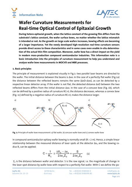
1. Basic principles<br />
The principle of measurement is explained visually in Fig.1: two parallel laser beams are directed to<br />
the wafer. The initial distance between the beams is Δxo. In the case of a perfectly flat wafer (Fig.1a)<br />
the distance between the reflected beams remains the same (ΔxD=Δxo), as can be detected by a<br />
respective linear detector array. If the wafer is not flat, the detected distance ΔxD between the two<br />
reflected beams differs from the initial distance Δxo. In the case of a concave bow (Fig. 1b), which<br />
can be defined by a positive radius of curvature RC>0, the distance decreases, whereas a convex bow<br />
(Fig. 1c) defined by a negative radius of curvature RC 2 m). Hence, a simple linear<br />
relationship between the measured distance of laser spots at the detector ΔxD and the bowing radius<br />
RC can be applied:<br />
C<br />
1<br />
X0<br />
ΔX<br />
Rc>0<br />
− Δx<br />
XD < X0<br />
D o<br />
= ≅<br />
≡<br />
(1)<br />
RC<br />
2Δx<br />
oZ<br />
D 2Δx<br />
oZ<br />
D<br />
ZD is the distance between wafer and detector. S is the raw signal, i.e. the magnitude of change in<br />
the laser spot distance by wafer bow with respect to a perfectly flat wafer. With C we define the pa-<br />
S<br />
X0<br />
Rc X0<br />
Page 1/4
In<strong>for</strong>mation Note<br />
rameter “curvature” calculated as the inverse of the bowing radius RC. We use C instead of RC because<br />
in this case we have a curvature of zero <strong>for</strong> a perfectly flat wafer instead of dealing with a<br />
(mathematically correct) infinitely large bowing radius of RC=∞. The curvature C is measured in units<br />
of [km -1 ] because the detected curvature in compound semiconductor technology is typically very<br />
small and, hence, the related radius of curvature is large (in the order of kilometers -1 ).<br />
The sensitivity of the method increases when the initial distance Δxo is larger (see Fig. 2). However,<br />
if the initial distance is too large, the size of the detector might be too small to detect both beams<br />
throughout the whole measurement. The range of curvature detectable is there<strong>for</strong>e limited by Δxo and decreases with increasing Δxo. X0 S<br />
X0 I SS = XD S- X0 S<br />
SI = XD I- X0 I<br />
Rc0<br />
Rc
In<strong>for</strong>mation Note<br />
• Some<strong>time</strong>s wafers show a radial bowing variation. In this case, accurate measurement<br />
can be guaranteed only if the beams are reflected exactly around the center of the wafers.<br />
• The distance between the wafers and the detector may slightly change depending on the<br />
reactor temperature. Accurate calibration is there<strong>for</strong>e needed at both, room temperature<br />
(where the wafers are loaded) and the growth temperature.<br />
LayTec has developed and optimized curvature optical heads that solve these problems in a variety<br />
of MOCVD and MBE systems, so that the user can focus on the curvature measurement.<br />
3. Four major effects contributing to the wafer bow during epitaxial growth:<br />
a) The specifics of the wafer polishing technology causes an initial bow of the wafer, which can be<br />
seen already after loading the bare substrate and gives a bow offset, which remains constant<br />
throughout the growth process.<br />
b) For MOCVD, a vertical temperature gradient is typical (cold-wall reactors): the back-side of the<br />
wafer is heated by the susceptor directly, whereas the top-side faces the 'cold wall' (shower head,<br />
ceiling) and is cooled due to the heat-transfer from the wafer surface to the cooled wall. The vertical<br />
temperature difference between wafer surface and back-side is rather small (~1...3K), but its contribution<br />
to wafer bow is usually considerable. The curvature changes with gas concentration and gas<br />
flow as Fig. 4 shows. Low ohmic substrates are less effected than high-omic ones due to their good<br />
thermal conductivity.<br />
Fig. 4: <strong>Curvature</strong> response (green) of a bare sapphire<br />
substrate in an AIX200/4RF-S reactor subjected to temperature<br />
changes (red) and total pressure changes (arrows)<br />
as typical <strong>for</strong> an LED process (here, however,<br />
without per<strong>for</strong>ming any growth!): the curvature of the<br />
bare sapphire substrate is following gradually the backside<br />
heating but additionally shows steep rises and falls<br />
whenever the surface cooling changes abruptly with<br />
total pressure (as indicated by the arrows).<br />
Fig. 5: Change of the bow (green) of GaN on sapphire<br />
when the temperature (red) changes from 1075°C to<br />
400°C: every change in the absolute temperature of the<br />
wafer causes significant changes in wafer curvature due<br />
to the different linear expansion coefficients between<br />
the substrate and the films.<br />
Version 20101216<br />
Page 3/4
In<strong>for</strong>mation Note<br />
c) After layers have been grown on the substrate, every change in the absolute temperature of the<br />
wafer causes significant changes in wafer curvature due to the different linear expansion coefficients<br />
between the substrate and the films. Fig. 5 demonstrates these changes of the bow <strong>for</strong> GaN /<br />
Sapphire when the temperature changes from 1075°C to 400°C.<br />
d) During growth of films under constant conditions (constant temperature is of the highest importance!)<br />
the curvature changes linearly in all non-lattice-matched (to the substrate) growth conditions.<br />
In Fig. 6 the growth rate of the film rf is measured <strong>time</strong> by analysing in-situ reflectance data at<br />
the same with the curvature measurements. The slope of curvature can be used to calculate lattice<br />
mismatch directly according to the well-known Stoney's equation (3):<br />
ΔC<br />
6Mf<br />
= − 2<br />
Δt<br />
h M<br />
s<br />
s<br />
af<br />
( T)<br />
− as(<br />
T)<br />
⋅rf<br />
⋅<br />
a ( T)<br />
This effect can be used <strong>for</strong> a composition analysis (see Chapter 4 below).<br />
All the four effects (a-d) contribute to the total wafer bow at a certain growth step of a compound<br />
semiconductor device structure. In consequence, their superposition should be analyzed alongside<br />
with systematical optimization of growth recipes <strong>for</strong> best lateral wafer temperature uni<strong>for</strong>mity (zero<br />
wafer-bow) in critical growth steps.<br />
4. Quantitative analysis of curvature measurements<br />
For quantitative analysis, however, we can focus<br />
on the last effect (d) only, because it is the slope<br />
and not the absolute magnitude of curvature that<br />
has to be used. Fig. 6 provides an example of Al-<br />
GaN and InGaN composition measurement applying<br />
Eq. (3) to real-<strong>time</strong> curvature data [1]: With<br />
increasing Al(In) content of AlGaN or InGaN ternary<br />
alloys, the lattice mismatch between the GaN<br />
buffer and the ternary alloy film increases - and so<br />
does the slope of bsolute value of curvature. The<br />
positive respectively negative sign of slope relates<br />
to the smaller or larger lattice constant of AlGaN<br />
or InGaN with respect to GaN. A quantitative<br />
analysis of the slope can there<strong>for</strong>e be used to determine<br />
the alloy composition already On-situ.<br />
Paper [1] by Brunner et al. is recommended <strong>for</strong><br />
further reading. In 2005 LayTec has successfully released its curvature sensor EpiCurve ® 0<br />
75<br />
50<br />
500 1000<br />
1) Al GaN<br />
0.14<br />
-3.4*10<br />
25<br />
TT – the first<br />
sensor world-wide that measures wafer bowing, true temperature and reflectance simultaneously!<br />
It allows accurate strain monitoring, precise wafer temperature and growth rate analysis already<br />
during growth.<br />
-3<br />
AlGaN layer thickness (nm)<br />
AIX2400G3/HT<br />
EpiCurveTT<br />
-2.0*10<br />
2) Al GaN<br />
0.076<br />
4) In GaN<br />
0.075 -3<br />
Δa /a : f ES<br />
relax.<br />
0<br />
-5<br />
3.1*10<br />
concave<br />
convex<br />
-10<br />
0 25 50 75 100<br />
-3<br />
3) In GaN/<br />
0.02<br />
In GaN<br />
0.08<br />
7.8*10<br />
InGaN layer thickness (nm)<br />
-3<br />
AIX200/4-RF-S<br />
HR-EpiCurveTT<br />
Fig. 6: AlGaN and InGaN composition measurement<br />
applying Eq. (3) to real-<strong>time</strong> curvature data.<br />
[1] F. Brunner, A. Knauer, T. Schenk, M. Weyers and J.-T. Zettler, Quantitative analysis of in-situ wafer bowing measurements<br />
<strong>for</strong> III-nitride growth on sapphire; submitted to J. of Cryst. Growth.<br />
s<br />
Norm. <strong>Curvature</strong> (1/km)<br />
(3)<br />
Version 20101216<br />
Page 4/4