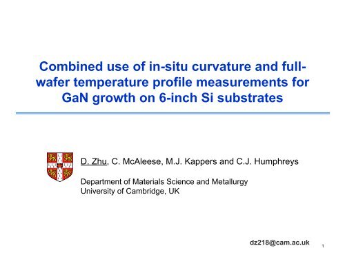
Combined use of in-situ curvature and full- wafer ... - Laytec
Combined use of in-situ curvature and full- wafer ... - Laytec
Combined use of in-situ curvature and full- wafer ... - Laytec

Create successful ePaper yourself
Turn your PDF publications into a flip-book with our unique Google optimized e-Paper software.
<strong>Comb<strong>in</strong>ed</strong> <strong>use</strong> <strong>of</strong> <strong>in</strong>-<strong>situ</strong> <strong>curvature</strong> <strong>and</strong> <strong>full</strong><strong>wafer</strong><br />
temperature pr<strong>of</strong>ile measurements for<br />
GaN growth on 6-<strong>in</strong>ch Si substrates<br />
D. Zhu, C. McAleese, M.J. Kappers <strong>and</strong> C.J. Humphreys<br />
Department <strong>of</strong> Materials Science <strong>and</strong> Metallurgy<br />
University <strong>of</strong> Cambridge, UK<br />
dz218@cam.ac.uk<br />
1
Motivation<br />
A potential low-cost manufactur<strong>in</strong>g route for GaN based solid-state light<strong>in</strong>g<br />
Advantages:<br />
Issues:<br />
� Availability <strong>of</strong> large size substrates at lower cost<br />
� Much lower fabrication costs <strong>of</strong> the devices<br />
� Compatibility with st<strong>and</strong>ard Si process<strong>in</strong>g equipment<br />
� Higher thermal conductivity than sapphire<br />
� Possibility <strong>of</strong> vertical contact LEDs on conduct<strong>in</strong>g silicon<br />
� Possibility <strong>of</strong> <strong>in</strong>tegrat<strong>in</strong>g electronics <strong>and</strong> optical devices<br />
� Large thermal expansion mismatch (Si: 54% that <strong>of</strong> GaN)<br />
� Large lattice mismatch (lattice constant Si: 17% less than GaN)<br />
Result<strong>in</strong>g <strong>in</strong>:<br />
� Tensile stra<strong>in</strong> <strong>and</strong> high dislocation density <strong>in</strong> epitaxial GaN<br />
� Wafer bow<strong>in</strong>g <strong>and</strong>/or crack<strong>in</strong>g, mak<strong>in</strong>g process<strong>in</strong>g difficult<br />
2
LED structure on Si substrate<br />
Schematic LED structures<br />
on Si substrates<br />
Mg-doped GaN<br />
InGaN/GaN MQW<br />
(Si-doped) GaN<br />
AlGaN buffer layer<br />
AlN nucleation layer<br />
Si (111) substrate<br />
MOVPE growth:<br />
� Stress control: AlGaN buffer<br />
In-<strong>situ</strong> monitor<strong>in</strong>g:<br />
� LayTec Epicurve ® TT: <strong>wafer</strong> <strong>curvature</strong>, true<br />
temperature <strong>and</strong> reflectance<br />
� Aixtron Argus: temperature pr<strong>of</strong>iler<br />
Ex-<strong>situ</strong> characterisation:<br />
� XRD: stra<strong>in</strong> state <strong>and</strong> quality, quantum well structure<br />
� TEM: TD analysis<br />
� AFM: Surface morphology <strong>and</strong> TD analysis<br />
� PL & EL: MQW <strong>and</strong> LED performance<br />
� Graphic-EYE: whole <strong>wafer</strong> optical imag<strong>in</strong>g<br />
� KSA Multi-Beam optical sensor (MOS) ultra-scan TM :<br />
ex-<strong>situ</strong> <strong>wafer</strong> <strong>curvature</strong><br />
3
In-<strong>situ</strong> <strong>curvature</strong> measurement - EpiCurve<br />
EpiCurve measurement pr<strong>in</strong>ciple<br />
(after LayTec Epicurve manual)<br />
Etalon<br />
Beam<br />
splitter<br />
Laser<br />
Susceptor<br />
Detector<br />
Wafer<br />
4
Curvature evolution dur<strong>in</strong>g growth <strong>of</strong> an LED structure on Si<br />
Process temperature (Tc)<br />
Curvature/km -1<br />
1200<br />
1000<br />
800<br />
600<br />
400<br />
200<br />
50<br />
0<br />
-50<br />
-100<br />
-150<br />
0<br />
0.00<br />
0 5000 10000 15000 20000<br />
0 5000 10000 15000 20000<br />
Time (s)<br />
Concave<br />
Convex<br />
0.40<br />
0.35<br />
0.30<br />
0.25<br />
0.20<br />
0.15<br />
0.10<br />
0.05<br />
Reflectance (a.u.)<br />
LayTec Epicurve ® TT<br />
After cool<strong>in</strong>g:<br />
Mg-doped GaN<br />
Si-doped GaN<br />
AlGaN<br />
AlN<br />
Si substrate<br />
5
More about stress control<br />
Curvature/km -1<br />
50<br />
0<br />
-50<br />
-100<br />
-150<br />
<strong>in</strong>-<strong>situ</strong> anneal<strong>in</strong>g<br />
AlN nucleation<br />
layer (300 nm)<br />
AlN nucleation<br />
layer (200 nm)<br />
AlGaN buffer (680 nm)<br />
Si-doped GaN (750 nm)<br />
AlGaN buffer (1.3 µm)<br />
InGaN-GaN<br />
MQW<br />
0 5000 10000 15000 20000<br />
Si-doped GaN (1.5 µm)<br />
Time (s)<br />
Cool<strong>in</strong>g<br />
InGaN-GaN<br />
MQW<br />
LED1<br />
LED2<br />
Concave<br />
Convex<br />
The optimised buffer layer thickness will depend on the thickness <strong>of</strong> GaN layer required<br />
QW active region was grown on a convex bowed <strong>wafer</strong>.<br />
Cool<strong>in</strong>g<br />
6
Graphic-EYE whole <strong>wafer</strong> optical imag<strong>in</strong>g<br />
Badly-cracked sample with extended<br />
cracks across the <strong>wafer</strong><br />
150 mm<br />
Cracks show up as bright l<strong>in</strong>es <strong>in</strong> the image with very strong contrast<br />
Crack-free GaN <strong>wafer</strong>s have been achieved<br />
Generally crack-free sample with cracks<br />
only at extreme edges <strong>of</strong> <strong>wafer</strong><br />
150 mm<br />
6 mm<br />
Courtesy <strong>of</strong> Q<strong>in</strong>etiQ<br />
7
Additional growth issues: slip <strong>in</strong> Si (111) <strong>wafer</strong>s<br />
Two sets <strong>of</strong> thermal stresses considered, aris<strong>in</strong>g from:<br />
Silicon <strong>wafer</strong><br />
Through-thickness temperature variations<br />
Radial temperature variations<br />
Stresses are resolved onto the various slip systems: {111} <br />
Radial temperature variations<br />
Through-thickness<br />
temperature<br />
variations<br />
At 1000 ºC, with a temperature difference <strong>of</strong> 10 ºC across the <strong>wafer</strong> thickness, the<br />
maximum stress <strong>and</strong> result<strong>in</strong>g <strong>curvature</strong> are calculated to be:<br />
0.4 MPa, 16 m for 2-<strong>in</strong>ch <strong>wafer</strong>, 275 µm thick<br />
0.6 MPa, 38 m for 6-<strong>in</strong>ch <strong>wafer</strong>, 650 µm thick<br />
not sufficient by itself to ca<strong>use</strong> slip – although it may enhance radial T variations.<br />
8
Wafer <strong>curvature</strong> change<br />
Temperature ( o C)<br />
ca<strong>use</strong>d by through-thickness temperature variations<br />
1100<br />
1000<br />
900<br />
800<br />
700<br />
600<br />
500<br />
400<br />
0 1000 2000 3000<br />
Time (s)<br />
Radius <strong>of</strong> <strong>wafer</strong> <strong>curvature</strong> changes from flat to ~30 m (concave) dur<strong>in</strong>g temperature<br />
ramp from room temperature to 1100 ºC<br />
40<br />
20<br />
0<br />
Curvature/km -1<br />
RT 1100 ºC<br />
9
Shear stress on the (1-11)[10-1] <strong>and</strong> (1-11)[0-1-1] slip system<br />
10 ºC Radial temperature variations<br />
Temperature ( o C)<br />
Temperature ( o C)<br />
1005<br />
1000<br />
995<br />
990<br />
1005<br />
1000<br />
995<br />
990<br />
Temperature pr<strong>of</strong>ile 1<br />
-10 0 10 20 30 40 50 60 70 80<br />
Radial distance (mm)<br />
Temperature pr<strong>of</strong>ile 2<br />
0 10 20 30 40 50 60 70 80<br />
Radial distance (mm)<br />
Wafer centre Wafer edge<br />
Max stress ~2 MPa<br />
Max stress ~1 MPa<br />
Stress calculations: courtesy <strong>of</strong><br />
Kirsten McLaughl<strong>in</strong>, Cambridge<br />
10
Monitor<strong>in</strong>g the temperature pr<strong>of</strong>ile across the whole <strong>wafer</strong><br />
Temperature ( o C)<br />
Aixtron Argus temperature pr<strong>of</strong>iler<br />
1200<br />
1000<br />
800<br />
600<br />
400<br />
Wafer centre<br />
Wafer edge<br />
200<br />
0 2000 4000 6000 8000<br />
Time (s)<br />
(d)<br />
Susceptor<br />
Si slips due to the temperature nonuniformity<br />
across the <strong>wafer</strong>, result<strong>in</strong>g <strong>in</strong><br />
very bowed <strong>wafer</strong>.<br />
Susceptor C B A B C<br />
Wafer<br />
1062<br />
1052<br />
1042<br />
1032<br />
1022<br />
1012<br />
1002<br />
992<br />
982<br />
972<br />
962<br />
Temperature ( o C)<br />
After Si slip<br />
1060<br />
1040<br />
1020<br />
1000<br />
980<br />
960<br />
940<br />
Centre<br />
Edge<br />
11
Ma<strong>in</strong>ta<strong>in</strong><strong>in</strong>g flat temperature pr<strong>of</strong>ile<br />
LayTec Epicurve ® TT<br />
Temperature ( o C)<br />
Temperature ( o C)<br />
1100<br />
1000<br />
900<br />
800<br />
700<br />
600<br />
500<br />
Aixtron Argus<br />
400<br />
0 5000 10000 15000<br />
1200<br />
1000<br />
800<br />
600<br />
400<br />
200<br />
Wafer centre<br />
Wafer edge<br />
Time (s)<br />
0 1 2 3 4<br />
Time (s)<br />
80<br />
60<br />
40<br />
20<br />
0<br />
-20<br />
-40<br />
-60<br />
-80<br />
-100<br />
-120<br />
Curvature/km -1<br />
Susceptor<br />
concave<br />
convex<br />
C B A B C<br />
6-<strong>in</strong>ch Si <strong>wafer</strong><br />
775<br />
770<br />
765<br />
760<br />
755<br />
750<br />
745<br />
740<br />
735<br />
730<br />
725<br />
Temperature ( o C)<br />
770<br />
760<br />
750<br />
740<br />
730<br />
Centre<br />
Edge<br />
12
GaN-based LED looks good on 6-<strong>in</strong>ch Si<br />
Picture <strong>of</strong> an InGaN-GaN blue-emitt<strong>in</strong>g LED structure grown<br />
on 6-<strong>in</strong>ch Si, this <strong>wafer</strong> is flat <strong>and</strong> completely crack-free.<br />
AFM image <strong>of</strong> p-GaN surface<br />
PL peak emission wavelength:<br />
Average: 448 nm;<br />
Std. Dev. 7 nm<br />
1 µm<br />
PL <strong>in</strong>tensity: Std. Dev. 12%<br />
EL: YES, over whole <strong>wafer</strong><br />
Wafer bow:
Electrolum<strong>in</strong>escence from 6-<strong>in</strong>ch LED <strong>wafer</strong><br />
D. Zhu et al., “GaN-based LEDs grown on 6-<strong>in</strong>ch diameter Si (111)<br />
substrates by MOVPE”, Proc. SPIE 7231, 723118 (2009)<br />
Processed at Q<strong>in</strong>etiQ<br />
Current (mA)<br />
Photo diode current (a.u.)<br />
30<br />
25<br />
20<br />
15<br />
10<br />
5<br />
0<br />
1.4<br />
1.2<br />
1.0<br />
0.8<br />
0.6<br />
0.4<br />
0.2<br />
0.0<br />
EL <strong>in</strong>tensity (a.u.)<br />
2500<br />
2000<br />
1500<br />
1000<br />
500<br />
0<br />
350 400 450 500 550 600 650<br />
Wavelength (nm)<br />
0 1 2 3 4<br />
Voltage (V)<br />
Photo diode current (a.u.)<br />
0.3<br />
0.2<br />
0.1<br />
0.0<br />
0 10 20 30 40 50 60 70<br />
Drive current (mA)<br />
0 100 200 300 400 500<br />
Drive current (mA)<br />
14
Summary<br />
� Flat <strong>and</strong> crack-free GaN-based LED structures have been grown on 6-<strong>in</strong>ch Si (111)<br />
substrates by MOVPE.<br />
� LayTec Epicurve ® TT was <strong>use</strong>d to measure the <strong>wafer</strong> <strong>curvature</strong> evolution dur<strong>in</strong>g the<br />
growth, <strong>and</strong> allows rapid optimisation <strong>of</strong> the AlGaN buffer layer for stress management.<br />
� Temperature pr<strong>of</strong>iles over <strong>full</strong> 6-<strong>in</strong>ch Si <strong>wafer</strong> were measured <strong>in</strong> real-time us<strong>in</strong>g Aixtron<br />
Argus <strong>in</strong>strument, show<strong>in</strong>g the changes across the <strong>wafer</strong> due to <strong>curvature</strong>. A flat<br />
temperature pr<strong>of</strong>ile can be ma<strong>in</strong>ta<strong>in</strong>ed over the <strong>full</strong> LED run by adjust<strong>in</strong>g the heater<br />
zone sett<strong>in</strong>gs accord<strong>in</strong>gly.<br />
� <strong>Comb<strong>in</strong>ed</strong> <strong>use</strong> <strong>of</strong> <strong>in</strong>-<strong>situ</strong> <strong>curvature</strong> <strong>and</strong> <strong>full</strong>-<strong>wafer</strong> temperature pr<strong>of</strong>ile measurements is<br />
very <strong>use</strong>ful for successful development <strong>of</strong> GaN growth on 6-<strong>in</strong>ch Si substrates.<br />
15
Acknowledgements<br />
� Project partners<br />
� Fund<strong>in</strong>g:<br />
PARSEM<br />
16