tle4270_V1_6.pdf - Infineon
tle4270_V1_6.pdf - Infineon
tle4270_V1_6.pdf - Infineon

Create successful ePaper yourself
Turn your PDF publications into a flip-book with our unique Google optimized e-Paper software.
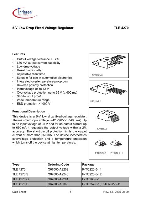
5-V Low Drop Fixed Voltage Regulator<br />
Features<br />
• Output voltage tolerance ≤ ±2%<br />
650 mA output current capability<br />
Low-drop voltage<br />
Reset functionality<br />
Adjustable reset time<br />
Suitable for use in automotive electronics<br />
Integrated overtemperature protection<br />
Reverse polarity protection<br />
Input voltage up to 42 V<br />
Overvoltage protection up to 65 V (≤ 400 ms)<br />
Short-circuit proof<br />
Wide temperature range<br />
ESD protection > 4000 V<br />
Functional Description<br />
This device is a 5-V low drop fixed-voltage regulator.<br />
The maximum input voltage is 42 V (65 V, ≤ 400 ms). Up<br />
to an input voltage of 26 V and for an output current up<br />
to 650 mA it regulates the output voltage within a 2%<br />
accuracy. The short circuit protection limits the output<br />
current of more than 650 mA. The device incorporates<br />
overvoltage protection and a temperature protection<br />
which turns off the device at high temperatures.<br />
P-TO220-5-11<br />
P-TO220-5-12<br />
P-TO263-5-1<br />
TLE 4270<br />
P-TO252-5-1 P-TO252-5-11<br />
Type Ordering Code Package<br />
TLE 4270 Q67000-A9209 P-TO220-5-11<br />
TLE 4270 S Q67000-A9243 P-TO220-5-12<br />
TLE 4270 G Q67006-A9201 P-TO263-5-1<br />
TLE 4270 D Q67006-A9360 P-TO252-5-1, P-TO252-5-11<br />
Data Sheet 1 Rev. 1.6, 2005-08-09
P-TO220-5-11<br />
(P-TO220-5-1)<br />
1<br />
Figure 1 Pin Configuration (top view)<br />
Table 1 Pin Definitions and Functions<br />
Pin Symbol Function<br />
5<br />
RO D<br />
Ι GND Q<br />
AEP01923<br />
P-TO220-5-12<br />
(P-TO220-5-2)<br />
TLE 4270<br />
1 I Input; block to ground directly at the IC with a ceramic capacitor.<br />
2 RO Reset Output; the open collector output is connected to the<br />
5-V output via an integrated resistor of 30 kΩ.<br />
3 GND Ground; internally connected to heatsink.<br />
1<br />
Ι<br />
GND Q<br />
RO D<br />
AEP02172<br />
1 5<br />
AEP01922<br />
4 D Reset Delay; connect a capacitor to ground for delay time adjustment.<br />
5 Q 5-V Output; block to ground with 22 µF capacitor, ESR < 3 Ω.<br />
Data Sheet 2 Rev. 1.6, 2005-08-09<br />
5<br />
P-TO263-5-1<br />
(P-TO220-5-8)<br />
Ι<br />
RO D<br />
GND<br />
GND<br />
Q<br />
P-TO252-5 (D-PAK)<br />
1 5<br />
Ι RO D Q<br />
AEP02580
Circuit Description<br />
TLE 4270<br />
The control amplifier compares a reference voltage, which is kept highly accurate by<br />
resistance adjustment, to a voltage that is proportional to the output voltage and drives<br />
the base of a series transistor via a buffer. Saturation control as a function of the load<br />
current prevents any over-saturation of the power element.<br />
The IC also incorporates a number of internal circuits for protection against:<br />
Overload<br />
Overvoltage<br />
Overtemperature<br />
Reverse polarity<br />
Application Description<br />
The IC regulates an input voltage in the range of 5.5 V < V I < 36 V to V Q,nom = 5.0 V. Up<br />
to 26 V it produces a regulated output current of more than 650 mA. Above 26 V the<br />
save-operating-area protection allows operation up to 36 V with a regulated output<br />
current of more than 300 mA. Overvoltage protection limits operation at 42 V. The<br />
overvoltage protection hysteresis restores operation if the input voltage has dropped<br />
below 36 V. A reset signal is generated for an output voltage of V Q < 4.5 V. The delay for<br />
power-on reset can be set externally with a capacitor.<br />
Data Sheet 3 Rev. 1.6, 2005-08-09
Adjustment<br />
Temperature<br />
Sensor<br />
Bandgap<br />
Reference<br />
Figure 2 Block Diagram<br />
Control<br />
Amplifier<br />
Buffer<br />
Saturation<br />
Control and<br />
Protection<br />
Circuit<br />
1<br />
5<br />
I Q<br />
3<br />
GND<br />
Reset<br />
Generator<br />
AEB01924<br />
TLE 4270<br />
Data Sheet 4 Rev. 1.6, 2005-08-09<br />
2<br />
4<br />
RO<br />
D
Table 2 Absolute Maximum Ratings<br />
T j = -40 to 150 °C<br />
Parameter Symbol Limit Values Unit Notes<br />
Input I<br />
Voltage<br />
Voltage<br />
Current<br />
Reset Output RO<br />
Voltage<br />
Current<br />
Reset Delay D<br />
Voltage<br />
Current<br />
Output Q<br />
Voltage<br />
Current<br />
Ground GND<br />
V I<br />
V I<br />
I I<br />
V RO<br />
I RO<br />
V D<br />
I D<br />
V Q<br />
I Q<br />
Min. Max.<br />
-42<br />
–<br />
–<br />
-0.3<br />
–<br />
-0.3<br />
–<br />
-1.0<br />
–<br />
Current I GND -0.5 – A –<br />
Temperatures<br />
Junction temperature<br />
Storage temperature<br />
T j<br />
T stg<br />
Table 3 Operating Range<br />
–<br />
-50<br />
TLE 4270<br />
Data Sheet 5 Rev. 1.6, 2005-08-09<br />
42<br />
65<br />
–<br />
7<br />
–<br />
7<br />
–<br />
16<br />
–<br />
150<br />
150<br />
Parameter Symbol Limit Values Unit Notes<br />
Min. Max.<br />
Input voltage V I 6 42 V –<br />
Junction temperature T j -40 150 °C –<br />
Thermal Resistance<br />
Junction ambient R thj-a – 65<br />
79<br />
V<br />
V<br />
–<br />
V<br />
–<br />
V<br />
–<br />
V<br />
–<br />
°C<br />
°C<br />
K/W<br />
K/W<br />
1) Mounted on PCB, 80 × 80 × 1.5 mm 3 ; 35µ Cu; 5µ Sn; Footprint only; zero airflow.<br />
–<br />
t ≤ 400 ms<br />
internally limited<br />
–<br />
Internally limited<br />
–<br />
Internally limited<br />
–<br />
Internally limited<br />
–<br />
–<br />
–<br />
TO263, TO252 1)<br />
Junction case R thj-c – 3 K/W TO-220/263<br />
Packages
Table 4 Characteristics<br />
V I = 13.5 V; -40 °C ≤ T j ≤ 125 °C (unless otherwise specified)<br />
Parameter Symbol Limit Values Unit Test Condition<br />
Min. Typ. Max.<br />
TLE 4270<br />
Output voltage V Q 4.90 5.00 5.10 V 5 mA ≤ I Q ≤ 550 mA;<br />
6 V ≤ V I ≤ 26 V<br />
Output voltage V Q 4.90 5.00 5.10 V 26 V ≤ V I ≤ 36 V;<br />
I Q ≤ 300 mA<br />
Output current<br />
limiting<br />
IQmax 650 850 – mA VQ = 0 V<br />
Current<br />
consumption<br />
Iq = II - IQ Iq – 1 1.5 mA IQ = 5 mA<br />
Current<br />
consumption<br />
Iq = II - IQ Iq – 55 75 mA IQ = 550 mA<br />
Current<br />
consumption<br />
Iq = II - IQ Iq – 70 90 mA IQ = 550 mA; VI = 5 V<br />
Drop voltage VDR – 350 700 mV IQ = 550 mA 1)<br />
Load regulation ∆VQ,Lo – 25 50 mV IQ = 5 to 550 mA;<br />
VI = 6 V<br />
Line regulation ∆VQ,Li – 12 25 mV VI = 6 to 26 V<br />
IQ = 5 mA<br />
Power supply Ripple<br />
rejection<br />
Reset Generator<br />
PSRR – 54 – dB f r = 100 Hz;<br />
V r = 0.5 Vpp<br />
Switching threshold VRT 4.5 4.65 4.8 V –<br />
Reset High voltage VROH 4.5 – – V –<br />
Reset low voltage V ROL – 60 – mV R int = 30 kΩ 2) ;<br />
1.0 V ≤ V Q ≤ 4.5 V<br />
Reset low voltage V ROL – 200 400 mV I R = 3 mA, V Q = 4.4 V<br />
Reset pull-up R int 18 30 46 kΩ internally connected<br />
to Q<br />
Charge current I D,c 8 14 25 µA V D = 1.0 V<br />
Data Sheet 6 Rev. 1.6, 2005-08-09
Table 4 Characteristics (cont’d)<br />
VI = 13.5 V; -40 °C ≤ Tj ≤ 125 °C (unless otherwise specified)<br />
Parameter Symbol Limit Values Unit Test Condition<br />
Min. Typ. Max.<br />
V DU 1.4 1.8 2.3 V –<br />
Upper reset timing<br />
threshold<br />
Lower reset timing<br />
threshold<br />
VDL 0.2 0.45 0.8 V VQ < VRT Delay time trd – 13 – ms CD = 100 nF<br />
Reset reaction time trr – – 3 µs CD = 100 nF<br />
Overvoltage Protection<br />
Turn-Off voltage V I, ov 42 44 46 V –<br />
TLE 4270<br />
1) Drop voltage = VI - VQ (measured when the output voltage has dropped 100 mV from the nominal value<br />
obtained at 13.5 V input)<br />
2) Reset peak is always lower than 1.0 V.<br />
Data Sheet 7 Rev. 1.6, 2005-08-09
V I<br />
Figure 3 Test Circuit<br />
Input<br />
Reset<br />
to µC<br />
Figure 4 Application Circuit<br />
II<br />
1000 µF<br />
470 nF<br />
470 nF<br />
I<br />
RO<br />
I<br />
1<br />
VD<br />
4<br />
D<br />
TLE 4270G<br />
ID<br />
CD<br />
1 5<br />
2<br />
TLE 4270<br />
3<br />
GND<br />
3<br />
2<br />
RO<br />
GND<br />
AES01925<br />
TLE 4270<br />
Data Sheet 8 Rev. 1.6, 2005-08-09<br />
5<br />
IGND<br />
4<br />
Q<br />
D<br />
Q<br />
I Q<br />
IR<br />
100 nF<br />
V R<br />
22 µF<br />
22 µF<br />
V Q<br />
5 V - Output<br />
AES01926
Design Notes for External Components<br />
TLE 4270<br />
An input capacitor C I is necessary for compensation of line influences. The resonant<br />
circuit consisting of lead inductance and input capacitance can be damped by a resistor<br />
of approx. 1 Ω in series with C I. An output capacitor C Q is necessary for the stability of<br />
the regulating circuit. Stability is guaranteed at values of C Q ≥ 22 µF and an ESR of<br />
< 3 Ω.<br />
Reset Circuitry<br />
If the output voltage decreases below 4.5 V, an external capacitor C D on pin 4 (D) will be<br />
discharged by the reset generator. If the voltage on this capacitor drops below V DL, a<br />
reset signal is generated on pin 2 (RO), i.e. reset output is set low. If the output voltage<br />
rises above the reset threshold, C D will be charged with constant current. After the<br />
power-on-reset time the voltage on the capacitor reaches V DU and the reset output will<br />
be set high again. The value of the power-on-reset time can be set within a wide range<br />
depending of the capacitance of C D.<br />
Reset Timing<br />
The power-on reset delay time is defined by the charging time of an external capacitor<br />
C D which can be calculated as follows:<br />
C D = (∆t × I D,c)/∆V (1)<br />
Definitions:<br />
C D = delay capacitors<br />
∆t = reset delay time t rd<br />
I D,c = charge current, typical 14 µA<br />
∆V = V DU , typical 1.8 V<br />
V DU = upper reset timing threshold at C D for reset delay time<br />
t rd = ∆V × C D/I D,c<br />
The reset reaction time t rr is the time it takes the voltage regulator to set the reset out<br />
LOW after the output voltage has dropped below the reset threshold. It is typically 1 µs<br />
for delay capacitor of 47 nF. For other values for C D the reaction time can be estimated<br />
using the following equation:<br />
t rr ≈ 20 s/F × C D<br />
Data Sheet 9 Rev. 1.6, 2005-08-09<br />
(2)<br />
(3)
VI<br />
V Q<br />
V D<br />
VRO<br />
VRT<br />
VDU<br />
VDL trd<br />
Figure 5 Reset Time Response<br />
t rr<br />
Power-ON Thermal<br />
Reset Shutdown<br />
TLE 4270<br />
AES01927<br />
Data Sheet 10 Rev. 1.6, 2005-08-09<br />
< trr<br />
Voltage Drop Under- Secondary Load<br />
at Input voltage Spike Bounce<br />
dV<br />
d t<br />
ID,<br />
c<br />
=<br />
C<br />
D
Output Voltage V Q versus<br />
Temperature T j<br />
VQ<br />
5.2<br />
V<br />
5.1<br />
5.0<br />
4.9<br />
4.8<br />
4.7<br />
V I = 13.5 V<br />
Output Current I Q versus<br />
Temperature T j<br />
1200<br />
mA<br />
I Q max<br />
AED01928<br />
4.6<br />
-40 0 40 80 120 ˚C 160<br />
T<br />
1000<br />
800<br />
600<br />
400<br />
200<br />
j<br />
AED01930<br />
0<br />
-40 0 40 80 120 ˚C 160<br />
T<br />
j<br />
Output Voltage V Q versus<br />
Input Voltage V I<br />
R L = 25 Ω<br />
Output Current I Q versus<br />
Input Voltage V I<br />
TLE 4270<br />
Data Sheet 11 Rev. 1.6, 2005-08-09<br />
VQ<br />
I Q<br />
12<br />
V<br />
10<br />
8<br />
6<br />
4<br />
2<br />
0<br />
0 2<br />
1.2<br />
A<br />
1.0<br />
0.8<br />
0.6<br />
0.4<br />
0.2<br />
T j<br />
4<br />
= 125 ˚C<br />
25 ˚C<br />
6 8<br />
V Ι<br />
AED01929<br />
V<br />
10<br />
AED03038<br />
0<br />
0 10 20 30 40<br />
V<br />
V 50<br />
I
Current Consumption I q versus<br />
Output Current I Q<br />
Ι q<br />
3<br />
mA<br />
2<br />
1<br />
0 0<br />
= 13.5 V<br />
Current Consumption I q versus<br />
Input Voltage V I<br />
I q<br />
120<br />
mA<br />
100<br />
80<br />
60<br />
40<br />
20<br />
VΙ<br />
AED03092<br />
20 40 60 80 mA 120<br />
R L = 10 Ω<br />
R L =<br />
20 Ω<br />
50 Ω<br />
Ι Q<br />
AED01934<br />
0<br />
0 10 20 30 40<br />
V<br />
V 50<br />
I<br />
Current Consumption I q versus<br />
Output Current I Q<br />
Drop Voltage V DR versus<br />
Output Current I Q<br />
TLE 4270<br />
Data Sheet 12 Rev. 1.6, 2005-08-09<br />
Ι q<br />
V DR<br />
80<br />
mA<br />
70<br />
60<br />
50<br />
40<br />
30<br />
20<br />
10<br />
0 0<br />
800<br />
mV<br />
700<br />
600<br />
500<br />
400<br />
300<br />
200<br />
100<br />
0<br />
0<br />
VΙ<br />
= 13.5 V<br />
AED03093<br />
100 200 300 400 mA 600<br />
T j = 125 ˚C<br />
25 ˚C<br />
Ι Q<br />
AED01935<br />
200 400 600 mA<br />
I<br />
1000<br />
Q
Charge Current I D,c versus<br />
Temperature T j<br />
I<br />
20<br />
µA<br />
18<br />
16<br />
14<br />
12<br />
10<br />
8<br />
6<br />
4<br />
-40<br />
I D, c<br />
V I = 13.5 V<br />
VD<br />
= 1 V<br />
AED03047<br />
0 40 80 120 ˚C 160<br />
T j<br />
TLE 4270<br />
Upper Reset Timing Threshold V DU<br />
versus Temperature T j<br />
Data Sheet 13 Rev. 1.6, 2005-08-09<br />
V DU<br />
4.0<br />
mA<br />
3.5<br />
3.0<br />
2.5<br />
2.0<br />
1.5<br />
1.0<br />
0.5<br />
0 -40<br />
VΙ<br />
= 13.5 V<br />
V DU<br />
AED03094<br />
0 40 80 120 ˚C 160<br />
T j
Package Outlines<br />
17±0.3<br />
15.65±0.3<br />
1)<br />
13.4<br />
0...0.15<br />
1)<br />
C<br />
9.8 ±0.15<br />
1.7<br />
10 ±0.2<br />
8.5 1)<br />
3.7-0.15 Figure 6 P-TO220-5-11 (Plastic Transistor Single Outline)<br />
±0.2<br />
2.8<br />
±0.3<br />
8.6<br />
A<br />
10.2 ±0.3<br />
0.8 ±0.1<br />
0.25 M<br />
Typical<br />
All metal surfaces tin plated, except area of cut.<br />
GPT09064<br />
TLE 4270<br />
Data Sheet 14 Rev. 1.6, 2005-08-09<br />
A<br />
C<br />
1.27±0.1<br />
0.05<br />
2.4<br />
4.4<br />
9.25 ±0.2<br />
8.4 ±0.4<br />
You can find all of our packages, sorts of packing and others in our<br />
<strong>Infineon</strong> Internet Page “Products”: http://www.infineon.com/products.<br />
SMD = Surface Mounted Device<br />
3.7±0.3<br />
0.5 ±0.1<br />
3.9 ±0.4<br />
Dimensions in mm
17±0.3<br />
15.65±0.3<br />
1)<br />
13.4<br />
C<br />
0...0.15<br />
Typical<br />
10 ±0.2<br />
9.8 ±0.15<br />
1.7<br />
8.5 1)<br />
3.7-0.15<br />
Figure 7 P-TO220-5-12 (Plastic Transistor Single Outline)<br />
±0.2<br />
2.8<br />
A<br />
6x<br />
0.8 ±0.1<br />
0.25 M<br />
1) All metal surfaces tin plated, except area of cut.<br />
GPT09065<br />
TLE 4270<br />
Data Sheet 15 Rev. 1.6, 2005-08-09<br />
A<br />
B<br />
C<br />
B<br />
1.27 ±0.1<br />
You can find all of our packages, sorts of packing and others in our<br />
<strong>Infineon</strong> Internet Page “Products”: http://www.infineon.com/products.<br />
SMD = Surface Mounted Device<br />
±0.5<br />
11<br />
13 ±0.5<br />
0.05<br />
2.4<br />
4.4<br />
9.25 ±0.2<br />
0.5 ±0.1<br />
Dimensions in mm
(15)<br />
9.25 ±0.2 1±0.3<br />
0...0.3<br />
5 x 0.8 ±0.1<br />
10<br />
0.25 M<br />
Figure 8 P-TO263-5-1 (Plastic Transistor Single Outline)<br />
±0.2<br />
8.5 1)<br />
1)<br />
7.55<br />
0...0.15<br />
4 x<br />
A<br />
1.7<br />
TLE 4270<br />
Data Sheet 16 Rev. 1.6, 2005-08-09<br />
A<br />
B<br />
4.7 ±0.5<br />
1.27 ±0.1<br />
B<br />
0.05<br />
±0.3<br />
2.7<br />
2.4<br />
0.1<br />
8˚ MAX.<br />
1) Typical<br />
Metal surface min. X = 7.25, Y = 6.9<br />
All metal surfaces tin plated, except area of cut.<br />
4.4<br />
0.5 ±0.1<br />
You can find all of our packages, sorts of packing and others in our<br />
<strong>Infineon</strong> Internet Page “Products”: http://www.infineon.com/products.<br />
SMD = Surface Mounted Device<br />
0.1 B<br />
GPT09113<br />
GPT09113<br />
Dimensions in mm
±0.5<br />
9.9<br />
6.22 -0.2<br />
1±0.1<br />
(4.17)<br />
0.15 max<br />
per side<br />
4.56<br />
6.5 -0.10<br />
+0.15<br />
5.4 ±0.1<br />
Figure 9 P-TO252-5-1 (Plastic Transistor Single Outline)<br />
±0.15<br />
0.8<br />
5x0.6<br />
1.14<br />
A<br />
±0.1<br />
0.25 M<br />
All metal surfaces tin plated, except area of cut.<br />
+0.05<br />
2.3 -0.10<br />
+0.08<br />
0.9 -0.04<br />
GPT09161<br />
TLE 4270<br />
Data Sheet 17 Rev. 1.6, 2005-08-09<br />
A<br />
B<br />
B<br />
1<br />
0...0.15<br />
You can find all of our packages, sorts of packing and others in our<br />
<strong>Infineon</strong> Internet Page “Products”: http://www.infineon.com/products.<br />
SMD = Surface Mounted Device<br />
0.51 min ±0.1<br />
+0.08<br />
0.5 -0.04<br />
0.1<br />
Dimensions in mm
5.7 MAX.<br />
±0.1<br />
9.98 ±0.5<br />
6.22 -0.2<br />
(4.24) 1<br />
1)<br />
0.15 MAX.<br />
per side<br />
4.56<br />
6.5<br />
+0.15<br />
-0.05<br />
1.14<br />
0.25 M A<br />
1) Includes mold flashes on each side.<br />
All metal surfaces tin plated, except area of cut.<br />
Figure 10 P-TO252-5-11 (Plastic Transistor Single Outline)<br />
(5)<br />
±0.15<br />
0.8<br />
A<br />
5 x 0.6<br />
±0.1<br />
0.1 B<br />
TLE 4270<br />
Data Sheet 18 Rev. 1.6, 2005-08-09<br />
B<br />
B<br />
0.9 -0.01<br />
+0.20<br />
0...0.15<br />
0.51 MIN.<br />
+0.05<br />
2.3 -0.10<br />
You can find all of our packages, sorts of packing and others in our<br />
<strong>Infineon</strong> Internet Page “Products”: http://www.infineon.com/products.<br />
SMD = Surface Mounted Device<br />
0.5<br />
0.5<br />
+0.08<br />
-0.04<br />
+0.08<br />
-0.04<br />
GPT09527<br />
Dimensions in mm
Remarks<br />
TLE 4270<br />
Data Sheet 19 Rev. 1.6, 2005-08-09
Edition 2005-08-09<br />
Published by <strong>Infineon</strong> Technologies AG,<br />
St.-Martin-Strasse 53,<br />
81669 München, Germany<br />
© <strong>Infineon</strong> Technologies AG 2004.<br />
All Rights Reserved.<br />
Attention please!<br />
The information herein is given to describe certain components and shall not be considered as a guarantee of<br />
characteristics.<br />
Terms of delivery and rights to technical change reserved.<br />
We hereby disclaim any and all warranties, including but not limited to warranties of non-infringement, regarding<br />
circuits, descriptions and charts stated herein.<br />
Information<br />
For further information on technology, delivery terms and conditions and prices please contact your nearest<br />
<strong>Infineon</strong> Technologies Office (www.infineon.com).<br />
Warnings<br />
Due to technical requirements components may contain dangerous substances. For information on the types in<br />
question please contact your nearest <strong>Infineon</strong> Technologies Office.<br />
<strong>Infineon</strong> Technologies Components may only be used in life-support devices or systems with the express written<br />
approval of <strong>Infineon</strong> Technologies, if a failure of such components can reasonably be expected to cause the failure<br />
of that life-support device or system, or to affect the safety or effectiveness of that device or system. Life support<br />
devices or systems are intended to be implanted in the human body, or to support and/or maintain and sustain<br />
and/or protect human life. If they fail, it is reasonable to assume that the health of the user or other persons may<br />
be endangered.