EKV v2.6 Model Structure
EKV v2.6 Model Structure
EKV v2.6 Model Structure

You also want an ePaper? Increase the reach of your titles
YUMPU automatically turns print PDFs into web optimized ePapers that Google loves.
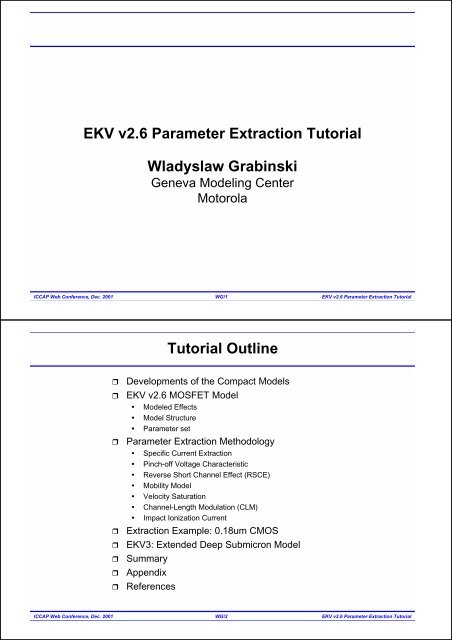
<strong>EKV</strong> <strong>v2.6</strong> Parameter Extraction Tutorial<br />
Wladyslaw Grabinski<br />
Geneva <strong>Model</strong>ing Center<br />
Motorola<br />
ICCAP Web Conference, Dec. 2001 WG/1<br />
<strong>EKV</strong> <strong>v2.6</strong> Parameter Extraction Tutorial<br />
Tutorial Outline<br />
Developments of the Compact <strong>Model</strong>s<br />
<strong>EKV</strong> <strong>v2.6</strong> MOSFET <strong>Model</strong><br />
<strong>Model</strong>ed Effects<br />
<strong>Model</strong> <strong>Structure</strong><br />
Parameter set<br />
Parameter Extraction Methodology<br />
Specific Current Extraction<br />
Pinch-off Voltage Characteristic<br />
Reverse Short Channel Effect (RSCE)<br />
Mobility <strong>Model</strong><br />
Velocity Saturation<br />
Channel-Length Modulation (CLM)<br />
Impact Ionization Current<br />
Extraction Example: 0.18um CMOS<br />
<strong>EKV</strong>3: Extended Deep Submicron <strong>Model</strong><br />
Summary<br />
Appendix<br />
References<br />
ICCAP Web Conference, Dec. 2001 WG/2<br />
<strong>EKV</strong> <strong>v2.6</strong> Parameter Extraction Tutorial
Developments of the Compact <strong>Model</strong>s<br />
No. of <strong>Model</strong> Parameters<br />
1000<br />
100<br />
10<br />
LEVEL1<br />
BSIM3v2<br />
BSIM3v3<br />
BSIM2<br />
BSIM3v2<br />
LEVEL2<br />
LEVEL3<br />
HSP28<br />
BSIM3v1<br />
BSIM<br />
PCIM<br />
HSP28<br />
BSIM3v3<br />
BSIM<br />
BSIM2<br />
BSIM4<br />
SP<br />
MM9 <strong>EKV</strong>3<br />
<strong>EKV</strong> <strong>v2.6</strong><br />
Including L,W,P scaling<br />
Without scaling<br />
1<br />
1960 1970 1980 1990 2000 2010<br />
Years<br />
Number of DC model parameters vs. the year of the introduction of the model<br />
Significant growth of the parameter number that includes geometry (W/L) scaling<br />
Most recent versions of the <strong>EKV</strong>, PCIM and SP models are included<br />
ICCAP Web Conference, Dec. 2001 WG/3<br />
<strong>EKV</strong> <strong>v2.6</strong> Parameter Extraction Tutorial<br />
<strong>EKV</strong> <strong>Model</strong> Versions<br />
1994: v2.0, first fully continuous model (12 parameters):<br />
continuous: weak/strong inversion, conduction/saturation<br />
symmetric forward/reverse operation: bulk reference<br />
drain current, capacitances, thermal noise, 1/f noise, NQS model<br />
mobility, velocity saturation, CLM, short-, narrow-channel effects<br />
1995: v2.3 (16 parameters):<br />
improved short-channel effects, added substrate current<br />
1996: new QS charge-conservative model (MOS-AK meeting, Nov. 96,Bremen)<br />
1997: <strong>v2.6</strong>, applicable to deep submicron (0.25um) (18 parameters):<br />
coherent charge-based modeling of: static, QS, NQS effects and thermal noise<br />
reverse short-channel effect (RSCE)<br />
includes matching (statistical circuit simulation)<br />
1999: <strong>v2.6</strong>, analytical NQS and polydepletion models<br />
2000: <strong>EKV</strong>3 introduction (MOS-AK meeting, May 2000, Lausanne)<br />
ICCAP Web Conference, Dec. 2001 WG/4<br />
<strong>EKV</strong> <strong>v2.6</strong> Parameter Extraction Tutorial
<strong>EKV</strong> <strong>v2.6</strong> in summary:<br />
<strong>EKV</strong> <strong>v2.6</strong> MOSFET <strong>Model</strong><br />
a physics based MOSFET model in the public domain.<br />
Design driven modeling concept dedicated<br />
to analog circuit simulation of submicron CMOS circuits.<br />
has < 20 intrinsic model parameters.<br />
used in industrial and academic design groups<br />
<strong>EKV</strong> <strong>v2.6</strong> available in major commercial circuit simulators:<br />
AMI-spice, Antrim-AMS, Aplac, Eldo-Accusim, Intosoft,<br />
Hsim, LTspice, MacSpice, Microsim-CapV, PSpice, NanoSpice,<br />
NG-spice, Saber, SmartSpice, Smash, Spice-Opus, Spectre,<br />
Star-HSpice, Synopsis, Spice3, WinSpice.<br />
on-going implementations:<br />
ADS & ICCAP, T-Spice,<br />
MINIMOS (TU Vienna), TRANZ-TRAN (TU Budapest)<br />
ICCAP Web Conference, Dec. 2001 WG/5<br />
<strong>EKV</strong> <strong>v2.6</strong> Parameter Extraction Tutorial<br />
<strong>EKV</strong> <strong>v2.6</strong> <strong>Model</strong>ed Effects<br />
Physics-based modeling of weak, moderate and strong inversion.<br />
Effects of substrate doping level, substrate effect.<br />
Vertical field dependent mobility.<br />
Common short-channel effects:<br />
velocity saturation<br />
channel length modulation (CLM)<br />
two-dimensional bulk charge-sharing for short-and narrow-channel effects<br />
reverse short-channel effect (RSCE)<br />
substrate current effects on drain conductance<br />
Short-distance matching for statistical circuit simulation.<br />
ICCAP Web Conference, Dec. 2001 WG/6<br />
<strong>EKV</strong> <strong>v2.6</strong> Parameter Extraction Tutorial
B D<br />
V S<br />
V G<br />
S<br />
V D<br />
<strong>EKV</strong> <strong>v2.6</strong> <strong>Model</strong> <strong>Structure</strong><br />
G<br />
DL/2 Leff DL/2<br />
y<br />
Bulk-reference, symmetric model structure.<br />
Drain current expression including drift and diffusion:<br />
I<br />
where:<br />
D<br />
ICCAP Web Conference, Dec. 2001 WG/7<br />
<strong>EKV</strong> <strong>v2.6</strong> Parameter Extraction Tutorial<br />
x<br />
V G<br />
VD<br />
'<br />
∞ '<br />
∞ '<br />
− QI<br />
− QI<br />
− QI<br />
∫ ( ) ⋅ dVCH<br />
= β ⋅ dVCH<br />
−<br />
C ∫ ( ) β (<br />
'<br />
'<br />
'<br />
V OX<br />
C V OX<br />
C V OX<br />
= β<br />
∫<br />
S<br />
β = µ ⋅C<br />
W<br />
eff<br />
OX<br />
Leff<br />
S<br />
D<br />
V S<br />
G<br />
I D<br />
S D<br />
B<br />
) ⋅ dV<br />
<strong>EKV</strong> <strong>v2.6</strong> <strong>Model</strong> <strong>Structure</strong><br />
A simple and useful relation can then be obtained between the inversion<br />
charge density and the surface potential in a differential form:<br />
dQ C = n ⋅ dψ<br />
Consequently, the <strong>EKV</strong> model can also be considered<br />
as a surface potential based model<br />
-Q I /C OX<br />
n V p<br />
0<br />
V s<br />
'<br />
I /<br />
i f -i r<br />
'<br />
OX<br />
strong inversion<br />
Schematic representation of the normalized inversion charge density<br />
as a function of the channel voltage.<br />
Pinch-off voltage VP used in calculation of currents and charges<br />
V d<br />
constant V G > V TO<br />
ICCAP Web Conference, Dec. 2001 WG/8<br />
<strong>EKV</strong> <strong>v2.6</strong> Parameter Extraction Tutorial<br />
S<br />
weak inversion<br />
V P<br />
V ch<br />
CH<br />
= I<br />
F<br />
− I<br />
R<br />
V D
<strong>EKV</strong> <strong>v2.6</strong> <strong>Model</strong> <strong>Structure</strong> (cont.)<br />
Physical model basis leads to accurate description of transconductance-to-current<br />
ratio at all current levels allows coherent derivation of all model quantities including<br />
static, dynamic and noise modeling aspects.<br />
Static <strong>Model</strong><br />
i r (V G , V S , V B )<br />
i f (V G , V S , V B ),<br />
Transconductance gms<br />
to current ration I D<br />
Dynamic <strong>Model</strong><br />
QX (ir , if )<br />
∂<br />
CXYZ<br />
=<br />
∂V<br />
QX<br />
ir<br />
, i<br />
YZ<br />
( f<br />
)<br />
Mobility <strong>Model</strong><br />
β = β 0 g(Q B ,Q I )<br />
Noise <strong>Model</strong><br />
S Nth (i r , i f )<br />
ICCAP Web Conference, Dec. 2001 WG/9<br />
<strong>EKV</strong> <strong>v2.6</strong> Parameter Extraction Tutorial<br />
18 Intrinsic <strong>Model</strong> Parameters:<br />
Normalization<br />
<strong>EKV</strong> <strong>v2.6</strong> Parameter set<br />
V<br />
t<br />
g<br />
ms<br />
∂I<br />
=<br />
∂V<br />
Purpose Name Description Units Example<br />
Process COX gate oxide capacitance per unit area F/m 2<br />
3.45E-3<br />
parameters XJ junction depth m 0.15E-6<br />
DW channel width correction M -0.05E-6<br />
DL channel length correction M -0.1E-6<br />
Doping & Mobility VTO long-channel threshold voltage V 0.55<br />
related parameters GAMMA body effect parameter V 1/2<br />
0.7<br />
PHI bulk Fermi potential (*2) V 0.8<br />
KP transconductance parameter A/V 2<br />
160E-6<br />
E0 vertical characteristic field for mobility reduction V/m 80E6<br />
UCRIT longitudinal critical field V/m 4.0E6<br />
Short- & narrow-channel LAMBDA depletion length coefficient (channel length modulation) - 0.3<br />
effect parameters WETA narrow-channel effect coefficient - 0.1<br />
LETA short-channel effect coefficient - 0.3<br />
Q0 reverse short-channel effect peak charge density A s/m 2<br />
ICCAP Web Conference, Dec. 2001 WG/10<br />
<strong>EKV</strong> <strong>v2.6</strong> Parameter Extraction Tutorial<br />
D<br />
S<br />
500E-6<br />
LK reverse short-channel effect characteristic length m 0.34E-6<br />
Substrate current IBA first impact ionization coefficient 1 / m 260E6<br />
related parameters IBB second impact ionization coefficient V / m 350E6<br />
IBN saturation voltage factor for impact ionization - 1.0
<strong>EKV</strong> <strong>v2.6</strong> Parameter Set (cont.)<br />
4 temperature parameters:<br />
Name Description Units Example<br />
TCV threshold voltage temperature coefficient V/K 1.0E-3<br />
BEX mobility temperature exponent - -1.5<br />
UCEX longitudinal critical field temperature exponent - 0.8<br />
IBBT temperature coefficient for IBB 1/K 9.0E-4<br />
2 noise parameters:<br />
Name Description Units Example<br />
KF flicker noise coefficient - 0<br />
AF flicker noise exponent - 1<br />
Completed with 3 matching parameters:<br />
Name Description Units Example<br />
AVTO area related threshold voltage mismatch parameter Vm - DEV=15E-9<br />
AKP area related gain mismatch parameter m - DEV=25E-9<br />
AGAMMA area related body effect mismatch parameter Vm) 1/2<br />
- DEV=10E-9<br />
ICCAP Web Conference, Dec. 2001 WG/11<br />
<strong>EKV</strong> <strong>v2.6</strong> Parameter Extraction Tutorial<br />
<strong>EKV</strong> <strong>v2.6</strong> DC Parameter Extraction Methodology<br />
PRELIMINARY<br />
EXTRACTION<br />
Extraction of<br />
DL , DW , RSH<br />
from several<br />
geometries<br />
WIDE<br />
LONG<br />
specific current<br />
measurement<br />
VP vs. VG<br />
VTO, GAMMA, PHI<br />
ID vs. VG<br />
KP , E0<br />
IB vs. VG<br />
IBA , IBB , IBN<br />
WIDE<br />
SHORT<br />
specific current<br />
measurement<br />
VP vs. VG<br />
VP LETA VP vs. vs. VG VG<br />
LETA<br />
LETA , Q0 , LK<br />
ID vs. VD<br />
UCRIT, LAMBDA<br />
NARROW<br />
LONG<br />
VP vs. VG<br />
WETA<br />
Parameter extraction methodology established for <strong>EKV</strong> <strong>v2.6</strong><br />
L<br />
specific current<br />
measurement<br />
NARROW<br />
SHORT<br />
final check<br />
and fine tuning<br />
Sequential task performed from an array of transistors in the W/L plane.<br />
ICCAP Web Conference, Dec. 2001 WG/12<br />
<strong>EKV</strong> <strong>v2.6</strong> Parameter Extraction Tutorial
Transconductance to currnet ratio<br />
in saturation:<br />
g<br />
ms<br />
× U<br />
I<br />
D<br />
t<br />
=<br />
Setting I D /I S to 1:<br />
1<br />
1 1<br />
+ 1 +<br />
4 2<br />
≅<br />
Specific Current Extraction<br />
1<br />
4<br />
1<br />
I<br />
+<br />
I<br />
D<br />
s<br />
0.<br />
618<br />
+<br />
1<br />
2<br />
ISPEC<br />
Specific current I SPEC corresponds to intersection of strong<br />
and weak inversion asymptotes<br />
Not affected by:<br />
CLM, high field mobility reduction, S/D extrinsic resistances<br />
ICCAP Web Conference, Dec. 2001 WG/13<br />
<strong>EKV</strong> <strong>v2.6</strong> Parameter Extraction Tutorial<br />
V G<br />
I B<br />
I S I B = = n⋅<br />
β ⋅U<br />
2<br />
Pinch-off Voltage Characteristic<br />
V S =V P<br />
2<br />
T<br />
ICCAP Web Conference, Dec. 2001 WG/14<br />
<strong>EKV</strong> <strong>v2.6</strong> Parameter Extraction Tutorial<br />
VTO<br />
PHI<br />
Pinch-off voltage measurement at constant current (I S /2)<br />
GAMMA<br />
Gate voltage VG is swept and VP =VS is measured at the source for a transistor<br />
biased in moderate inversion and saturation
Short- and Narrow-Channel Effects on V p-V g<br />
VTO<br />
LETA<br />
WETA<br />
Effects of short- and narrow-channels are analysed using<br />
the charge-sharing approach.<br />
Corresponding parameters: LETA and WETA.<br />
ICCAP Web Conference, Dec. 2001 WG/15<br />
<strong>EKV</strong> <strong>v2.6</strong> Parameter Extraction Tutorial<br />
Reverse Short Channel Effect (RSCE)<br />
0.5um CMOS example 0.25um CMOS example<br />
Defect enhanced diffusion during fabrication leads to RSCE.<br />
RSCE is modeled as a change in the threshold voltage depending on L eff<br />
Only two model parameters Q0 and LK.<br />
ICCAP Web Conference, Dec. 2001 WG/16<br />
<strong>EKV</strong> <strong>v2.6</strong> Parameter Extraction Tutorial
Mobility <strong>Model</strong><br />
Influence of KP and E0 on the transfer characteristics, respectively<br />
Good behaviour for mobility reduction for both channel types.<br />
Substrate effect is correctly accounted for.<br />
No back-bias dependence required.<br />
ICCAP Web Conference, Dec. 2001 WG/17<br />
<strong>EKV</strong> <strong>v2.6</strong> Parameter Extraction Tutorial<br />
Velocity Saturation<br />
Influence of UCRT on the output characteristics<br />
A high lateral electric field in the channel causes the carrier velocity to saturate<br />
and limits the drain current.<br />
Parameter UCRIT accounts for this effect.<br />
ICCAP Web Conference, Dec. 2001 WG/18<br />
<strong>EKV</strong> <strong>v2.6</strong> Parameter Extraction Tutorial
Channel-Length Modulation (CLM)<br />
Influence of LAMBDA on the output characteristics<br />
The relative channel length reduction depends on the pinch-off point<br />
in the MOSFET channel near drain end.<br />
Depletion length coefficient (LAMBDA) models CLM effect.<br />
ICCAP Web Conference, Dec. 2001 WG/19<br />
<strong>EKV</strong> <strong>v2.6</strong> Parameter Extraction Tutorial<br />
Impact Ionization Current<br />
Influence of IBA and IBB on the substrate current, respectively<br />
The substrate current is treated as a component of the total extrinsic current:<br />
I D = I DS + I DB<br />
Substrate current affects the total extrinsic conductances, in particular<br />
drain conductance (g DS ).<br />
ICCAP Web Conference, Dec. 2001 WG/20<br />
<strong>EKV</strong> <strong>v2.6</strong> Parameter Extraction Tutorial
Transconductance to Current Ratio<br />
0.5um CMOS example 0.25um CMOS example<br />
Excellent match from weak through moderate to strong inversion regions.<br />
Measurement and simulation comparisons show that gms /ID ratio<br />
is technology independent.<br />
ICCAP Web Conference, Dec. 2001 WG/21<br />
<strong>EKV</strong> <strong>v2.6</strong> Parameter Extraction Tutorial<br />
CV <strong>Model</strong>ing Example<br />
CV characteristics (C gg, C gd, C gs, G gb) of a large MOSFET<br />
as function the the gate to bulk bias (V D=V S=0)<br />
Consistent model for all charges and capacitances (G,D,S,B).<br />
Capacitances are valid in all operating regions, continuous,<br />
and symmetrical at V DS =0<br />
ICCAP Web Conference, Dec. 2001 WG/22<br />
<strong>EKV</strong> <strong>v2.6</strong> Parameter Extraction Tutorial
Drain Current Id<br />
Conductance gds<br />
Drain Voltage Vd<br />
Drain Voltage Vd<br />
Extraction Example: 0.18um CMOS<br />
Drain Current Id<br />
Output current: I d vs. V d characteristics<br />
Conductance gds<br />
Drain Voltage Vd<br />
Output conductance: g ds vs. V d characteristics<br />
ICCAP Web Conference, Dec. 2001 WG/23<br />
<strong>EKV</strong> <strong>v2.6</strong> Parameter Extraction Tutorial<br />
Conductance gds<br />
Drain Current Id<br />
Drain Voltage Vd<br />
Drain Voltage Vd Drain Voltage Vd<br />
<strong>EKV</strong>3: Extended Deep Submicron <strong>Model</strong><br />
Advances in <strong>EKV</strong>3 compact modeling include:<br />
polydepletion effect<br />
quantum-mechanics QM effects<br />
extended charge-based mobility model<br />
enhanced velocity saturation/CLM model (charge-based)<br />
improved short-channel effects: DIBL, weak inversion slope<br />
extended reverse short channel effect (RSCE) model<br />
second order short/narrow channel effects<br />
gate current model<br />
gate induced drain leakage (GIDL)<br />
NQS effects<br />
short-channel thermal noise<br />
ICCAP Web Conference, Dec. 2001 WG/24<br />
<strong>EKV</strong> <strong>v2.6</strong> Parameter Extraction Tutorial
Summary<br />
The <strong>EKV</strong> <strong>v2.6</strong> model and related parameter extraction methodology<br />
have been developed at Electronics Lab of EPFL<br />
Design driven MOSFET modeling concept is dedicated to analog<br />
circuit simulation of the advanced CMOS circuits.<br />
The model is well suited for direct and optimization based extraction<br />
as well as for statistical modeling tasks<br />
On-line model documentation at: http://legwww.epfl.ch/ekv<br />
Complete DC and CV <strong>EKV</strong> <strong>v2.6</strong> model code is available<br />
as generic c-code, and also in spice3 and Verilog-A formats<br />
The <strong>EKV</strong>3 developments are carried out by international modeling<br />
team: EPFL Switzerland, NTUA Greece, ENSPS France<br />
ICCAP Web Conference, Dec. 2001 WG/25<br />
<strong>EKV</strong> <strong>v2.6</strong> Parameter Extraction Tutorial<br />
Acknowledgements<br />
C. Enz, F. Krummenacher, E.Vittoz<br />
Authors of the initial <strong>EKV</strong> paper<br />
M. Bucher, J-M. Sallese, C. Lallement, F. Theodoloz<br />
<strong>EKV</strong> Development Team<br />
F. Krummenacher, M. Bucher,<br />
Smart Silicon Systems (S3)<br />
C.McAndrew, L.Lemaitre, O. Pilloud, J. Victory<br />
GMC, Motorola<br />
M.Mierzwinski, F. Sischka<br />
Agilent<br />
All developers implementing the <strong>EKV</strong> model into<br />
public domain and commercial simulation tools<br />
ICCAP Web Conference, Dec. 2001 WG/26<br />
<strong>EKV</strong> <strong>v2.6</strong> Parameter Extraction Tutorial
Appendix<br />
The <strong>EKV</strong> intrinsic model parameters can roughly be estimated from Spice level 2/3 parameters as indicated in the table below, if<br />
no parameter extraction facility is available. Attention has to be paid to units of the parameters. This estimation method can be<br />
helpful and generally gives reasonable results. Nevertheless be aware that the underlying modeling in Spice level 2/3 and in the<br />
<strong>EKV</strong> model is not the same, even if the names and the function of several parameters are similar. Therefore it is preferred if<br />
parameter extraction is made directly from measurements.<br />
NAME UNITS DEFAULT EXAMPLE ’LOWER’ ’UPPER’ ESTIMATION<br />
COX F/m 2<br />
0.7E-3 3.45E-3 - - εSi / TOX<br />
XJ m 0.1E-6 0.15E-6 0.01E-6 1E-6 XJ<br />
DL m 0 -0.15*Lmin -0.5*Lmin 0.5*Lmin XL – 2 LD<br />
DW m 0 -0.1*Wmin -0.5*Wmin 0.5*Wmin XL – 2WD<br />
VTO V 0.5 0.7 0 2 VTO<br />
GAMMA V 1/2<br />
1.0 0.7 0 2 (2qεsi NSUB) 1/2 COX<br />
PHI V 0.7 0.5 0.3 2 2Vt ln(NSUB/ni)<br />
KP A/V2 50E-6 150E-6 10E-6 - U0 COX<br />
E0 V/m 1.0E12 200E6 0.1/(0.4 TOX) - 0.2/(THETA TOX)<br />
UCRIT V/m 2.0E6 2.3E6 1.0E6 25E6 VMAX/UO<br />
LAMBDA - 0.5 0.8 0 3 -<br />
LETA - 0.1 0.3 0 2 -<br />
WETA - 0.25 0.2 0 2 -<br />
Q0 As/m 2<br />
0.0 230E-6 0 - -<br />
LK m 0.29E-6 0.4E-6 0.05E-6 2E-6 -<br />
IBA 1/m 0.0 2.0E8 0.0 5.0E8 ALPHA VCR / LC<br />
IBB V/m 3.0E8 2.0E8 1.8E8 4.0E8 VCR/LC<br />
IBN - 1.0 0.6 0.4 1.0 -<br />
εox = 0.0345E-9 F/m, q = 1.609E-19 C, k = 1.381E-23 J/K Lc = ε Si XJ / COX<br />
ε si = 0.104E-9 F/m n i = 1.45E16 m -3 V t = kT/q = 0.0259 V (at room temperature)<br />
NOTE: Parameters in this table suppose m (meter) has been chosen as length unit. L min and W min are the minimum drawn<br />
length and width of the transistors. Example values are indicated for enhancement N-channel devices.<br />
ICCAP Web Conference, Dec. 2001 WG/27<br />
<strong>EKV</strong> <strong>v2.6</strong> Parameter Extraction Tutorial<br />
References<br />
1.C. Enz, F. Krummenacher, E. Vittoz, 'An analytical MOS transistor model valid in all regions of Operation and dedicated to low-voltage and low-current applications',<br />
Journal on Analog Integrated Circuits and Signal Processsing, Kluwer Academic Publishers, pp. 83-114, July 1995<br />
2.C. Lallement, F. Pêcheux, Y. Hervé, 'VHDL-AMS Design of a MOST <strong>Model</strong> Including Deep Submicron and Thermal-Electronic Effects', 2001 IEEE International<br />
Workshop on Behavioral <strong>Model</strong>ing and Simulation BMAS 2001 October 10-12, 2001 FountainGrove Inn Santa Rosa, California, USA<br />
3.M. Bucher, J.-M. Sallese, C. Lallement, "Accounting for Quantum Effects and Polysilicon Depletion in an Analytical Design-Oriented MOSFET <strong>Model</strong>", Simulation<br />
of Semiconductor Processes and Devices 2001, pp. 296-299, Eds.D. Tsoukalas, C. Tsamis, Springer Vienna, NewYork, ISBN 3-211-83708-6<br />
4.J.-M. Sallese, "Advancements in DC and RF MOSFET <strong>Model</strong>ing with the EPFL-<strong>EKV</strong> Charge Based <strong>Model</strong>", Special session: MOS Transistor: Compact <strong>Model</strong>ing<br />
and Standardization Aspects, 8th International Conference MIXDES 2001, Zakopane, Poland, June 21-23, 20001.<br />
5.W. Grabinski "Compact <strong>Model</strong>ing of Low-power and RF Analogue MOSFET Devices", Special session: MOS Transistor: Compact <strong>Model</strong>ing and Standardization<br />
Aspects, 8th International Conference MIXDES 2001, Zakopane, Poland, June 21-23, 20001.<br />
6.D. Binkley, M. Bucher, D. Foty, 'Design-Oriented Characterization of CMOS over the Continuum of Inversion Level and Channel Length', Proc. 7th IEEE Int. Conf.<br />
on Electronics, Circuits & Systems ICECS'2k, pp. 161-164, Kaslik, Lebanon, Dec. 17-20, 2000.<br />
7.W. Grabinski, M. Bucher, J.-M. Sallese, F. Krummenacher, 'Compact <strong>Model</strong>ing of Ultra Deep Submicron CMOS Devices', ICSES'2000, October 17-20, 2000, Ustron,<br />
Poland.<br />
8.W. Grabinski, M. Bucher, J.-M. Sallese, F. Krummenacher, 'Advanced Compact <strong>Model</strong>ing of the Deep Submicron Technologies', Diagnostic and Yield, D&Y'2000,<br />
June 28-30, 2000, Warsaw, Poland.<br />
9.F. Krummenacher, W. Grabinski, M. Bucher, 'Advances in RF CMOS <strong>Model</strong>ing Based on the EPFL-<strong>EKV</strong> <strong>Model</strong>', Workshop on RF CMOS Transceivers, Pavia, June<br />
20-21, 2000<br />
10.J.-M. Sallese, A.-S. Porret, 'A novel approach to charge-based non-quasi-static model of the MOS transistor valid in all modes of operation', Solid State Electronics,<br />
Volume 44, No 6, pp. 887-894, June 2000.<br />
11.J.-M. Sallese, M. Bucher, C. Lallement, 'Improved Analytical <strong>Model</strong>ling of Polysilicon Depletion for CMOS CircuitSimulation', Solid State Electronics, Volume 44,<br />
No 6, pp. 905-912, June 2000.<br />
12.W.Grabinski, M. Bucher, F. Krummenacher, 'Harmonic Distortion Analysis Based on the EPFL-<strong>EKV</strong> <strong>Model</strong>', Silicon RF-IC: <strong>Model</strong>ing and Simulation Workshop<br />
24-25 February 2000, EPFL, Lausanne, Switzerland<br />
13.J.-M. Sallese, M. Bucher, C. Lallement, W. Grabinski, 'Advances in AC <strong>Model</strong>ing of MOSFET Using <strong>EKV</strong> Formalism', Silicon RF-IC: <strong>Model</strong>ing and Simulation<br />
Workshop 24-25 February 2000, EPFL, Lausanne.<br />
14.M. Bucher, 'Analytical MOS Transistor <strong>Model</strong>ling for Analog Circuit Simulation', Ph.D. Thesis No. 2114 (1999), Swiss Federal Institute of Technology, Lausanne<br />
ICCAP Web Conference, Dec. 2001 WG/28<br />
<strong>EKV</strong> <strong>v2.6</strong> Parameter Extraction Tutorial
References<br />
15.M. Bucher, J.-M. Sallese, C. Lallement, W. Grabinski, C. C. Enz, F. Krummenacher, 'Extended Charges <strong>Model</strong>ing for Deep Submicron CMOS', Int. Semicond.<br />
Device Research Symp. (ISDRS'99), Charlottesville, Virginia, December 1-3, 1999.<br />
16.F. Krummenacher, W. Grabinski, M. Bucher, 'RF MOSFET modeling approach based on the EPFL-<strong>EKV</strong> model', International workshop on low power RF<br />
integrated circuits, Lausanne, 19-20 October 1999<br />
17.W. Grabinski, M. Bucher, F. Krummenacher, 'The <strong>EKV</strong> Compact MOSFET <strong>Model</strong> and its Low-Power Analog and RF Applications', Proc. XXIInd Nat. Conf. on<br />
Circuit Theory and Electronic Networks, KKTOIUE'99, pp. 265-270, Stare<br />
Jablonki, Poland, October 20-23, 1999.<br />
18.W. Grabinski, M. Bucher, F. Krummenacher, 'The <strong>EKV</strong> <strong>Model</strong> Parameter Extraction Based on its IC-CAP USERC Implementation', HP-IC-CAP Users Meeting,<br />
Marseille, France, June 17, 1999.<br />
19.C. Enz, Y. Cheng, 'MOS Transistor <strong>Model</strong>ing Issues for RF Circuit Design', Workshop on Advances in Analogue Circuit Designs, Nice, March 1999.<br />
20.M. Bucher, W. Grabinski, '<strong>EKV</strong> MOS Transistor <strong>Model</strong>ling & RF Application', HP-RF MOS <strong>Model</strong>ling Workshop, Munich, February 15-16, 1999<br />
21.L. Portmann, C. Lallement, F. Krummenacher, 'A High Density Integrated Test Matrix of MOS transistors for Matching Study', ICMTS 1998. 1998 IEEE<br />
International Conference on Microelectronic Test <strong>Structure</strong>s, Proceedings IEEE,pp.19-24, 1998;<br />
22.M. Bucher, C. Lallement, C. Enz, F. Théodoloz, F. Krummenacher, 'Scalable GM/I Based MOSFET <strong>Model</strong>' Proc. 1997 Int. Semiconductor Device Research<br />
Symposium (ISDRS'97), pp. 615-618, Charlottesville, VA, USA, December 10-13, 1997.<br />
23.C. Lallement, M. Bucher, C. Enz, '<strong>Model</strong>ling and characterization of non-uniform substrate doping', Solid-State-Electronics. vol. 41: (12), pp. 1857-1861 Dec. 1997,<br />
24.C. Enz, E.A. Vittoz, 'MOS transistor modeling for low-voltage and low-power analog IC design' Microelectronic Engineering 39: (1-4) 59-76, Sp. Iss. SI Dec. 1997<br />
25.M. Bucher, C. Lallement, C. Enz, F. Krummenacher, 'Accurate MOS modelling for analog circuit simulation using the <strong>EKV</strong> model' 1996 IEEE International<br />
Symposium on Circuits and Systems Circuits and Systems Connecting the World, ISCAS 96, pp. 703-6 vol.4, 1996.<br />
26.C. Lallement, C. Enz, M. Bucher. 'Simple solutions for modelling the non-uniform substrate doping', 1996 IEEE International Symposium on Circuits and Systems.<br />
Circuits and Systems Connecting the World, ISCAS 96, pp. 436-9 vol.4, 1996;<br />
27.M. Bucher, C. Lallement, C. Enz 'An efficient parameter extraction methodology for the <strong>EKV</strong> MOST model', ICMTS 1996. 1996 IEEE International Conference on<br />
Microelectronic Test <strong>Structure</strong>s, Proceedings IEEE, pp.145-50, 1996;<br />
28.G.A.S. Machado, C. Enz, M. Bucher, 'Estimating key parameters in the <strong>EKV</strong> MOST model for analogue design and simulation' , 1995 IEEE Symposium on Circuits<br />
and Systems IEEE, New York, NY, USA; 3 vol. l+2346 pp. p.1588-91 vol.3. 1995;<br />
ICCAP Web Conference, Dec. 2001 WG/29<br />
<strong>EKV</strong> <strong>v2.6</strong> Parameter Extraction Tutorial