DFI Lanparty DK P45-T2R / Plus BIOS Setting Guideline
DFI Lanparty DK P45-T2R / Plus BIOS Setting Guideline
DFI Lanparty DK P45-T2R / Plus BIOS Setting Guideline

Create successful ePaper yourself
Turn your PDF publications into a flip-book with our unique Google optimized e-Paper software.
<strong>DFI</strong> <strong>Lanparty</strong> <strong>DK</strong> <strong>P45</strong>-<strong>T2R</strong> / <strong>Plus</strong><br />
<strong>BIOS</strong> <strong>Setting</strong> <strong>Guideline</strong><br />
(<strong>BIOS</strong> version: 2008/08/12) V001<br />
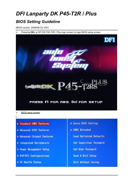
Pressing DEL at <strong>DFI</strong> <strong>DK</strong> <strong>P45</strong>-<strong>T2R</strong> / <strong>Plus</strong> logo screen to login <strong>BIOS</strong> setup screen<br />
<strong>BIOS</strong> setup screen<br />
L
Advance <strong>BIOS</strong> mode : Press F9 at main setup screen to swap to advance mode<br />
Genie <strong>BIOS</strong> settings: This setup thread is combined all needed settings for over clocking<br />
(CPU speed setting, CPU features, DRAM timings, Voltage settings and PCI speed etc.)
Genie <strong>BIOS</strong> : Main setup screen<br />
Exist Setup Shutdown: Mode1/Mode2<br />
Somehow it’s a “characteristic” of Intel chipset when overclocking… it will shutdown after tweaking. For that, <strong>DFI</strong><br />
has 2 different modes to chose:<br />
Mode 1) when the system was boot-up, it will run a little “diagnose”.<br />
If the CPU frequency doesn’t change too much, it will skip the “shutdown” function and rewrite the clock generator<br />
directly.<br />
Mode 2) no matter how little the CPU clock or DRAM’s ratio has been changed,<br />
The system still “shutdown” and reboot by itself<br />
Shutdown after AC Loss: Enable/Disable<br />
System Power recovers item. (Enabled for power on system automatically if AC power failure)<br />
OC Fail Retry Counter: 0~3 times<br />
OC fail retry looping setting. For example, set it on 1, it will retry boot again if fail, then auto back CPU default<br />
value to boot system.<br />
OC Fail CMOS reload: Disable / Bank1~3<br />
Assign bank settings reload for boot when OC fail<br />
CPU Clock ratio:<br />
CPU multiplier setting, 6~11 for locked processors, 6~50 times for unlocked processors
CPU Clock range:<br />
Boot-up clock: Auto/ 200MHz ~510MHz<br />
This function can help you out for setting a lower boot up clock. As a buffer, when your FSB is tweaked<br />
too high in the beginning. The process will to be: system boot up with “Boot-up clock” first, after that it<br />
will change to your highest FSB.<br />
CPU Clock Amplitude :<br />
Clock output strength, to add it for increasing grow weaker signal to terminal devices, default value is<br />
700mV, max out put is 1000mv.<br />
CPU Clock Skew0 :<br />
The skew of clock signal for CPU; To achieve higher FSB, please add more ps for increasing CPU OC<br />
ability. Default value is 0mV, max out put is 1500mv.<br />
*** Recommend to add 100ps~200ps when if the FSB is higher to 450~600MHz or DRAM speed at<br />
1800~2000MHz<br />
CPU Clock Skew1 :<br />
The skew of clock signal for North-Bridge; To achieve higher FSB, please add more ps for increasing<br />
CPU OC ability. Default value is 0mV, max out put is 1500mv.<br />
DRAM Speed:<br />
PCIE Clock : 100MHz~250MHz
CPU Feature:<br />
(For gaining a maximum CPU utilization, we will always disable all CPU key features except “Core<br />
multi-Processing”)<br />
DRAM Timing:<br />
Enhance Data Transmitting: Auto / Normal / First / Turbo<br />
<strong>DFI</strong> specifically designed a “fine-tune mode” for DATA transmitting performance, Normal for lowest<br />
performance, Fast for highest performance, Default AUTO will automatically adjust performance based<br />
on current system Front Side <strong>BIOS</strong>.<br />
Enhance Addressing: Auto / Normal / First<br />
<strong>DFI</strong> specifically designed a “fine-tune mode” for DATA addressing, “Normal” for lowest performance,<br />
“Fast” for highest performance, Default AUTO will automatically adjust performance based on current<br />
system Front Side <strong>BIOS</strong>.<br />
T2 Dispatch: Auto/ Enabled / Disabled<br />
DRAM performance parameters patch, enabling for getting optimized and disabling to relax DRAM
timing for running higher working frequency on modules.<br />
Performance level:<br />
It is tRD of DRAM parameter<br />
Read delay phase adjust:<br />
It is the fine-tune feature for tRD<br />
CLK setting fine delay:<br />
DLL and RCOMP <strong>Setting</strong>s: Auto/By Menu<br />
DRAM DLL table is a base for calculating clock delays; they are very important parameters for control<br />
singles delivering between CPU, NB and DRAM. Genie <strong>BIOS</strong> has provided 7 models to make more<br />
suitable parameters for running higher DDR2 speed.<br />
RCOMP Values is NB chipset register, it is impedance relating, change it will help to match signal<br />
requirement when run into a higher DRAM speed.<br />
*** Recommend fine delay and RCOMP settings for DRAM Ratio when OC to 450~600MHz ***<br />
DRAM ration @ 333:667, 266/667<br />
CH1/ CH2/ RCOMP <strong>Setting</strong>: 3/ 3/ 1, 5 /5 /1<br />
DRAM ration @ 400:800, 333:800,<br />
CH1/ CH2/ RCOMP <strong>Setting</strong>: 0/ 0/ 2
Fine Delay Step Degree:<br />
Scale gap from 10ps ~160ps, each scale can be able to adjust 31 degree steps.<br />
How to use it?<br />
For example: if you would like to manual set 310ps for DIMM1 Clock fine delay<br />
Fine Delay Step Degree=10ps<br />
DIMM 1 Clock Fine Delay=31 DEG<br />
For reaching 620ps, just need to change “Fine Delay Step Degree=20ps”<br />
Ch1 / Ch2 Clock Crossing <strong>Setting</strong>:<br />
Auto / More aggressive /aggressive / Nominal / Relaxed / More Relaxed<br />
Giving an easy explanation, after the CPU, PCIE, DRAM locked the clock phase by “PLL phase locked<br />
loop”, we can utilize the DRAM DLL to adjust DRAM operating phase by tuning DRAM DATA output<br />
phase forward or backward to create a better match with current DATA operating phase.<br />
The <strong>BIOS</strong> will automatically calculate a parameter after system boot up.<br />
The <strong>BIOS</strong> will show the current value of this parameter.<br />
The best tuning range for finding the best DATA operating phase will be 3 ranks before or after this<br />
current value.<br />
Ch1Ch2 CommonClock <strong>Setting</strong>:<br />
Auto / More aggressive /aggressive / Nominal / Relaxed / More Relaxed<br />
As above, it is PLL fine-tune for Common clock signals of DRAM modules.<br />
Ch1/Ch2 RDCAS GNT-Chip Delay: Auto /1~7 CLK<br />
Read command rate, 1Clock is Intel Command rate 1N mode, 2~7Clock are 1N disable mode<br />
Ch1/Ch2 WRCAS GNT-Chip Delay: Auto /1~7 CLK<br />
Write command rate, 1Clock is Intel Command rate 1N mode, 2~7Clock are 1N disable mode<br />
Ch1/Ch2 Command to CS Delay: Auto /1~7 CLK<br />
DRAM module bank selecting command rate, 1Clock is Intel Command rate 1N mode, 2~7Clock are 1N<br />
disable mode<br />
Common CMD to CS Timing”<br />
DRAM command rate mode 1N and 2N (1N disable) selection.
Voltage <strong>Setting</strong>s:<br />
CPU VID Special Add: (+12.5mV~+787.5mV)<br />
DRAM Voltage range: (1.789V~3.280V)<br />
SB Core / CPU PLL voltage: (1.55V~2.15V)<br />
These two voltages are controlling by same adjustable circuit, increasing CPU PLL voltage higher is<br />
better for gaining a stable OC situation.
NB Core Voltage: (1.265V~2.040V)<br />
CPU VTT Voltage range: (1.10V~1.60V)<br />
Vcore drop control: Enable / Disabled<br />
Enabling to control Vout level by PWM, disabling to get a maximum output.<br />
Clockgen voltage control: (3.45V~3.85V)<br />
Clock working voltage, increase it to achieve higher and more stable in extreme FSB environment<br />
GTL+ buffer Strength: Strong / Weak<br />
It is adjustment option for North-Bridge reference voltage strength.<br />
Host Slew Rate: Strong / Weak<br />
It is adjustment option for North-Bridge voltage driving strength.<br />
GTL REF Voltage control: Enable / Disabled<br />
CPU VTT reference voltage for determining host bus high / low level.<br />
FSB REF: AUTO<br />
MCH parameter registers for reaching highest FSB. Some of CPU can broken FSB wall after modified<br />
following values.<br />
*** Recommend settings ***<br />
Value: AUTO /23 /24 /26
<strong>BIOS</strong> Reloaded function: <strong>DFI</strong> Lan Party series are providing 1last fine status + 4 user’s profile<br />
space for doing <strong>BIOS</strong> setting saving and recovery.<br />
Auto Save bootable setting: Enable / Disable<br />
For saving last fine/ bootable parameters by <strong>BIOS</strong> itself every time<br />
Load last bootable:<br />
For loading last <strong>BIOS</strong> parameters.<br />
Save setting to bank with: Current settings or last saved CMOS settings.<br />
To define the resource of parameters for bank saving.<br />
User define setting bank #1 ~ #4:<br />
1. Bank Description: There are 4 rows for writing a short description. Double click on row when this<br />
row is empty, it will erase pervious data.<br />
2. Save to this bank: Press “Y” to save data to this bank<br />
3. Load from this bank: Press “Y” to load data of this bank to be current <strong>BIOS</strong> setup settings.<br />
4. Hotkey =>: define the “hotkey” for quick change <strong>BIOS</strong> settings to boot. Please press Hotkey after<br />
power on system immediately.
EZ Clear CMOS methods:<br />
a. EZ clear jumper<br />
b. To hold Home key to power on system, <strong>BIOS</strong> will recover FSB to default, remains setting will be<br />
keeping the last time fine status.<br />
c. To hold Insert key to power on system, <strong>BIOS</strong> will load all setting back to default as like doing a<br />
CCMOS by manually.<br />
End


![CP900-B [RoHS] - Dfi](https://img.yumpu.com/18888557/1/184x260/cp900-b-rohs-dfi.jpg?quality=85)
![CP900-B [RoHS] - Dfi](https://img.yumpu.com/18888555/1/184x260/cp900-b-rohs-dfi.jpg?quality=85)
![CP900-B [RoHS] - Dfi](https://img.yumpu.com/18888549/1/184x260/cp900-b-rohs-dfi.jpg?quality=85)
![CP900-B [RoHS] - Dfi](https://img.yumpu.com/18888536/1/184x260/cp900-b-rohs-dfi.jpg?quality=85)